Perfect light trapping in nanoscale thickness semiconductor films with resonant back reflector and spectrum-splitting structures
Abstract
The optical absorption of nanoscale thickness semiconductor films on top of light-trapping structures based on optical interference effects combined with spectrum-splitting structures is theoretically investigated. Nearly perfect absorption over a broad spectrum range can be achieved in nm thick films on top of one-dimensional photonic crystal or metal films. This phenomenon can be attributed to interference induced photonic localization, which enhances the absorption and reduces the reflection of the films. Perfect solar absorption and low carrier thermalization loss can be achieved when the light-trapping structures with wedge-shaped spacer layer or semiconductor films are combined with spectrum-splitting structures.
pacs:
78.66.-w,78.67.Pt,88.40.H-To reduce carbon dioxide release and cope with the increasing energy demand, photovoltaic solar cells have attracted significant attention. However, the cost efficiency and power conversion efficiency of solar cells is still relatively low. The high cost is mainly due to the use of expensive semiconductor materials, such as thick crystalline silicon films B98AG ; B13IMD . The efficiency is primarily limited by thermalization loss B98AG ; B13IMD ; NM12AP .
A best way to enhance cost efficiency is to reduce solar cells to nanoscale B13IMD ; JAP12SM ; S13JW ; NC13GM ; JAP13DBT ; NL14SS ; NP13PK to reduce material usage. In solar cells, the carrier collection length should be shorter than the carrier diffusion length (i.e., the distance travelled by a carrier before recombination). Thus nanoscale solar cells can use low-cost materials with lower carrier diffusion length (e.g., CuO, FeS2, and organic materials) to further reduces the cost JAP12SM . However, nanoscale materials are usually too thin to completely absorb the solar light. Plasmon, photonic crystal, and quasi-random nanostructures can enhance absorption JAP12SM ; NM12KV ; NC13ERM ; EES12VR ; EES11EEC ; APL12AB ; OE12MYK ; JAP13MR ; AM13QG ; JMCA14SE ; OE12SKK ; EES14KXW . Many theoretical and experimental works on interference-based light-trapping structures have demonstrated further improvement of the absorption of ultra-thin films compared with traditional light-trapping structures NM13MAK ; AM14HS ; APL13XLZ at the cost of reduced working frequency range. Perfect broadband absorption is still difficult to achieve in these structures.
Carrier thermalization loss results from energy mismatch between the photon energy and the bandgap of semiconductors B98AG ; B13IMD ; NM12AP . Photons with energy below the bandgap of semiconductors are not absorbed, while photons with energy above the bandgap can create only a maximum open-circuit voltage . The excess energy is converted to heat loss, where is the electron charge B98AG ; B13IMD ; NM12AP . Multijunction solar cells can reduce carrier thermalization loss with increased number of junctions. However, only 2- and 3-junction solar cells can be used for industrial production due to the limitation of lattice matching and current matching requirement B13IMD ; NM12AP . Another widely studied and demonstrated technque to reduce the thermalization loss is to use side-by-side subcells and a spectrum-splitting structure NM12AP ; SEM04AGI ; PP09AB ; PP10MAG , which directs solar light of different wavelengths to different subcells with different bandgaps . The thermalization loss can be reduced to approximately 10% by using 8-10 different subcells NM12AP .
In this letter, we show that by combining two distinct well-established techniques, the interference-based light-trapping structures and the spectrum-splitting structure, perfect broadband solar absorption can be achieved in nanoscale thickness semiconductor films (SFs). First, for the 32nm GaAs films on top of a light-trapping structure, numerical and analytical results show narrow-band resonant absorption exceeding 90% ( nine times larger than that of suspended GaAs films) as a result of photon localization. Second, we match the resonant absorption of the light-trapping structure with the spectrum-splitting structure by using wedge-shaped spacer layer or SFs and demonstrates perfect broadband solar absorption in nm thick SFs.
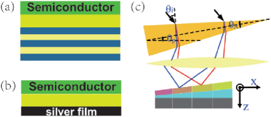
The light-trapping structure consists of a SF on top of a spacer layer and a one-dimensional photonic crystal (1DPC) [Fig. 1(a)] or 130 nm thick Ag film [Fig. 1(b)] at the bottom as the resonant back reflector. As demonstrated previously, such structure without wedge-shaped spacer layer or SFs can greatly enhance the absorption of graphene, MoS2, and ultra-thin SFs within a certain wavelength regionAM14HS ; APL13XLZ ; APL07KC ; APL12JTL ; EPL13NMRP ; NL12BSR ; APL12DH ; JAP14JTL . We also should point out the physical mechanism is different with the proposed structures consisting of thick SFs on photonic crystal OE07PB ; OE08JGM . The optical interference effects in thick SFs are unimportant due to the strong absorption and an antireflection coating layer must be used to reduce the reflection. The 1DPC is composed of 8.5 periods of alternating doped ZnS and SiO2 layers. The refractive indices of ZnS and SiO2 at nm are and , respectively. The permittivities for silver film and SFs are frequency dependent AP85EDP ; B99SA . All layers are nonmagnetic (). The thickness of the ZnS (SiO2) layers is (), where is the center wavelength. The spectrum-splitting structure is composed of a dense flint ZF13 prism and a low-dispersion convex lens [Fig. 1(c)]. The refractive indices for ZF13 glass is , where , and .
To model the absorption of SFs in this structure, the standard transfer matrix method is used APL12JTL ; JAP14JTL . In the lth layer, the electric field of the TE mode light with incident angle is given by
| (1) |
and the magnetic field of the TM mode in the lth layer is given by
| (2) |
where is the wave vector of the light, is the unit vectors in the x direction, and is the position of the lth layer in the z direction.
The electric fields of TE mode or the magnetic fields of TM mode in the (l+1)th layer are related to the incident fields by the transfer matrix utilizing the boundary condition
| (3) |
Thus, we can obtain the absorbance of lth layer using the Poynting vector APL12JTL ; JAP14JTL
| (4) |
where and [ and ] are the incident and outgoing Poynting vectors (l-1)th [(l+1)th] layer, respectively, is the incident Poynting vectors in air. For a perfect reflecting mirror without a spacer layer, straightforward algebra gives the absorptance
| (5) |
where ; ; and are the refractive index and thickness of SFs, respectively; and is the wave vector in the SFs. For thick metal film mirrors without the spacer layer, the absorptance
| (6) |
where , , , , , and , are the refractive indices of metal films.
For the spectrum-splitting structure, the angle of refraction of light through a prism is given by
| (7) |
where is the prism vertex angle, is the light incidence angle to the prism. The the light incidence angle to the convex lens is , where is the prism tilt angle. For perfect lens, the light are focused at , where is the focal length of the lens. For actual convex lens with aberrations, each of the refraction of light through the lens can be solved numerically using the Snell’s Law.
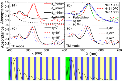
As shown in Fig. 2(a), for 32 nm (96 nm) GaAs films, the maximum absorbance at the resonant wavelength nm of solar radiation is improved by the 1DPC from 10.8% (28.4%) for suspended films to 90.8% (95.5%) even without antireflection coating layers. The magnitude of the enhancement is much larger than that of thick SFs on photonic crystal even with antireflection coating layersOE07PB ; OE08JGM . This is because the SFs act as a 1D surface defect that leads to localization on the surface due to interference effects [Figs. 2(e) and 2(f)], thereby reducing the reflection and enhancing the absorption APL12JTL ; NL12BSR ; JAP14JTL , similar to graphene and monolayer MoS2 on top of 1DPC. As shown in Fig. 2(b), the 1DPC with increasing number of periods has increasing reflectivity, photonic localization, and hence absorption. The SF resonant absorption with the 1DPC is close to that with a perfect reflection mirror (black solid circles) and slightly better than that with a Ag film (blue solid line and blue open circle), which has a lower reflectivity. However, the width of the resonant absorption for 1DPC is smaller than that for Ag film, due to the limited photonic band gap of the 1DPC. Away from the resonant absorption, the SF absorption on the Ag film almost coincides with that on a perfect reflection mirror.
For oblique light incidence, the large refractive index of GaAs ensures, by Snell’s law, that the light propagation angle in the GaAs film is small even with a large incident angle . Thus the resonant absorption wavelength for the SFs on the 1DPC is less affected by the light incident angle [Figs. 2(c) and 2(d)] and favors the design of solar cells.
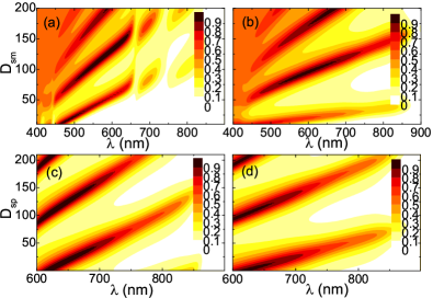
An essential ingredient of our proposal is the tunability of the resonant absorption wavelength of the light-trapping structure. As shown in Figs. 3(a) and 3(b), for the 1DPC, () decreases with decreasing SF thickness . This remains qualitatively true for the Ag film, since we still have the estimate . Another approach to tune is to insert a transparent (e.g., AlAs) spacer layer, e.g., for the 100 nm GaAs film on the 1DPC with and Ag films, almost linearly increases with the thickness of the spacer layer [Figs. 3(c) and 3(d)]. The spacer layer can also act as the buffer layer to enhance or reduce the lattice distortion of the SFs.
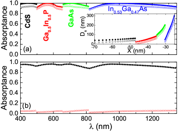
The problem with a given light-trapping structure is that enhanced absorption appears only within a certain range of wavelength. To cure this problem, we propose to combine it with the spectrum-splitting structure, which has been widely used experimentally to reduce the carrier thermalization loss in solar cells NM12AP ; SEM04AGI ; PP09AB ; PP10MAG . With the spectrum-splitting structure, a dense flint ZF13 prism and a low-dispersion convex lens focuses solar light with different wavelengths onto different locations on the SFs of the light-trapping structure [Fig. 1(c)]. By appropriately choosing the species and thicknesses of SFs or the thicknesses of the spacer layers to match the solar wavelength on each location (i.e., use the wedge-shaped spacer layer or SFs), perfect absorption can be achieved for each wavelength. Since the slope of the SFs is smaller than , the SF surface can be treated as parallel planes at each point. Thus, the transfer matrix method can be used in the calculation. The parameters include [Fig. 1(c)]: the prism vertex angle , the light incidence angle (the refracted light in the prism is parallel to bottom plane of the prism), the prism tilt angle (the light is nearly parallel to z direction), and the refractive indices and spherical radius of the convex lens are 1.5 and 0.6 m, respectively. CdS ( eV), Ga0.5In0.5P( eV), GaAs( eV), and In0.53Ga0.47As ( eV) films consist of side-by-side SFs.
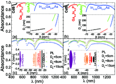
Numerical results are shown in Fig. 4. When the thickness of SFs perfectly matches the spectrum splitting with various (i.e., for lights with wavelength focused at point, the SF thickness at is chosen to obtain maximum absorption), the absorption of side-by-side SFs is almost always % and the maximum absorption can be %. Furthermore, more types of SFs can be used in this structure because the lattice matching and current matching requirements are not restricted. Thus, the proposed structures can significantly reduce carrier thermalization loss. Apart from applications in solar cells, perfect wide-range absorption can also have applications in optoelectronic devices, such as photoelectric detectors. Different for nanowire array solar cells, the proposed structures have low surface recombination loss. For SFs with linearly varied thickness [solid line in the inset of Figs. 4(a) and 4(b)], only the absorption of In0.53Ga0.47As film significantly decreases because the dispersion of ZF13 glass is too small to effectively separate different-wavelength lights within this wavelength range.
The influence of lens aberrations on SFs absorption is shown in Figs. 4(c) and 4(d). An actual convex lens cannot focus parallel light to a perfect point because of lens aberrations, which increase with increased lens diameter [inset of Figs. 4(c) and 4(d)]. Lens aberrations reduce the light-trapping effect because obtaining the maximum absorption from the entire whole focused light spot is difficult by varying the thickness of SFs. The influence of lens aberrations is reduced when spectrum-splitting structure with strong dispersion ability is used. The changes in SFs absorption are very small for cm. The absorption of GaAs and In0.53Ga0.47As significantly decreases for cm because of the low dispersion of ZF13 glass within the long wavelength range.
Perfect absorption can be achieved in the full solar spectrum by varying the spacer-layer thickness. Side-by-side SFs consist of 80 nm CdS, 80 nm Ga0.5In0.5P, 240 nm GaAs, and 240 nm In0.53Ga0.47As films. The refractive indices of a spacer layer is 2.6. The absorptance of SFs combined with spectrum-splitting structure can exceed 90% by varying spacer-layer thickness [Fig. 5(a)]. The thickness of SFs do not have to satisfy . SFs with a large absorption coefficient can be thinner. The influence of indium tin oxide transparency electrode on top of SFs is shown in Fig. 5(b). The absorptance of 20 nm indium tin oxide films is about 5%, and the absorptance of SFs shows about 5% reduction.
Finally, we discuss on the fabrication techniques and the potential improvement of the proposed structures. The length of the subcells is about 0.5-2 cm. The subcells can be fabricated separately and then joined using fasteners, adhesive, or welding. In each subcells, for SFs on top of 1DPC (which can be regarded as a half of the semiconductor microcavity) or metal films with spacer layers, similar structure have been fabricated in experiments AM14HS . The difference in this letter is that the SFs or spacer layers are wedge-shaped layers, which can be grown by existing technology such as molecular beam epitaxy. As shown by J. P. Prineas et al.APL06JPP , to reduce the speed of light 210 wedge-shaped semiconductor layers are grown by molecular beam epitaxy. Even though strong light-trapping effects is observed in the proposed structures, to achieve perfect absorption in nm SFs, light-trapping structure with more strong photonic localization such as the microcavity should be used PRB12AF ; OL12MAV . For the proposed spectrum-splitting structure, dispersion ability within the long wavelength range is low because of the low dispersion of ZF13 glass that degrades performance. Prism and convex lens without an antireflection film can reflect about 10-15% solar light. Thus, various types of spectrum-splitting structure should be studied in the future NM12AP ; SEM04AGI ; PP09AB ; PP10MAG .
In conclusion, the optical absorption of SFs on top of 1DPC and Ag films combination with spectrum-splitting structure is investigated. In these structures, the maximum optical absorptance of 100 nm SFs can be because of photon localization. The absorption of SFs on 1DPC is less affected by the incident angle of light and can be tuned by varying thickness of the SFs and spacer layers. By using side-by-side nanoscale thickness SFs and combination with spectrum-splitting structure, perfect solar absorption can be achieved with low carrier thermalization loss. Our proposal can have significant applications in the development of ultra-thin and high-efficiency solar cells and in optoelectronic devices, such as photoelectric detector.
We would like to thank Nianhua Liu for fruitful discussion. This work was supported by the NSFC (Grant Nos. 11364033, 11274036, 11322542, and 11104232), the MOST (Grant No. 2014CB848700), the NSF from the Jiangxi Province (Grant No. 20122BAB212003), and Science and Technology Project of Education Department of Jiangxi Province (Grant No. GJJ13005).
References
- (1) Adolf Goetzberger and Joachim Knobloch, editors. Crystalline Silicon Solar Cells. John Wiley & Sons, Chichester, 1998.
- (2) I. M. Dharmadasa, editor. Advances in thin-film solar cells. Pan Stanford Publishing, Boca Raton, 2012.
- (3) Albert Polman and Harry A. Atwater. Photonic design principles for ultrahigh-efficiency photovoltaics. Nature Materials, 11:174–177, 2012.
- (4) S. Mokkapati and K. R. Catchpole. Nanophotonic light trapping in solar cells. J. Appl. Phys., 112:101101, 2012.
- (5) Jesper Wallentin, Nicklas Anttu, Damir Asoli, Maria Huffman, Ingvar Åerg, Martin H. Magnusson, Gerald Siefer, Peter Fuss-Kailuweit, Frank Dimroth, Bernd Witzigmann, H. Q. Xu, Lars Samuelson, Knut Deppert, and Magnus T. Borgströ. Plasmonic-enhanced organic photovoltaics: Breaking the 10% efficiency barrier. Science, 339:1057–1060, 2013.
- (6) Giacomo Mariani1, Adam C. Scofield, Chung-Hong Hung, and Diana L. Huffaker. Gaas nanopillar-array solar cells employing in situ surface passivation. Nature Communications, 4:1497, 2013.
- (7) Daniel B. Turner-Evans, Christopher T. Chen, Hal Emmer, William E. McMahon, and Harry A. Atwater. Optoelectronic analysis of multijunction wire array solar cells. J. Appl. Phys., 114:014501, 2013.
- (8) Sunil Sandhu, Zongfu Yu, and Shanhui Fan. Detailed balance analysis and enhancement of open-circuit voltage in single-nanowire solar cells. Nano Lett., 14:1011–1015, 2014.
- (9) Peter Krogstrup, Henrik Ingerslev Jøgensen, Martin Heiss, Olivier Demichel, Jeppe V. Holm, Martin Aagesen, Jesper Nygard1, and Anna Fontcuberta i Morral. Single-nanowire solar cells beyond the shockley cqueisser limit. Nature Photonics, 7:306–310, 2013.
- (10) Kevin Vynck, Matteo Burresi, Francesco Riboli, and Diederik S.Wiersma. Photon management in two-dimensional disordered media. Nature Materials, 11:1017–1022, 2012.
- (11) Emiliano R. Martins, Juntao Li, YiKun Liu, Vale rie Depauw, Zhanxu Chen, Jianying Zhou, and Thomas F. Krauss. Deterministic quasi-random nanostructures for photon control. Nature Communications, 4:2665, 2013.
- (12) Veronika Rinnerbauer, Sidy Ndao, Yi Xiang Yeng, Walker R. Chan, Jay J. Senkevich, John D. Joannopoulos, Marin Soljačićab, and Ivan Celanovicb Show Affiliations. Recent developments in high-temperature photonic crystals for energy conversion. Energy Environ. Sci., 5:8815–8823, 2012.
- (13) Mauricio E. Calvo, Silvia Colodrero, Nuria Hidalgo, Gabriel Lozano, Carmen López-López, Olalla Sánchez-Sobradoa, and HernánMíguez. Porous one dimensional photonic crystals: novel multifunctional materials for environmental and energy applications. Energy Environ. Sci., 4:4800–4812, 2011.
- (14) A. Basch, F. J. Beck, T. Söderström, S. Varlamov, and K. R. Catchpole. Gaas nanopillar-array solar cells employing in situ surface passivation. Appl. Phys. Lett., 100:243903, 2012.
- (15) M. Y. Kuo, J. Y. Hsing, T. T. Chiu, C. N. Li, W. T. Kuo, T. S. Lay, and M. H. Shih. Quantum efficiency enhancement in selectively transparent silicon thin film solar cells by distributed bragg reflectors. Opt. Express, 20:A828–A835, 2012.
- (16) Ma’ayan Rumbak, Iris Visoly-Fisher, and Rafi Shikler. Broadband absorption enhancement via light trapping in periodically patterned polymeric solar cells. J. Appl. Phys., 114:013102, 2013.
- (17) Qiaoqiang Gan, Filbert J. Bartoli, and Zakya H. Kafafi. Plasmonic-enhanced organic photovoltaics: Breaking the 10% efficiency barrier. Adv. Mater., 25:2385–2396, 2013.
- (18) Sergey Eyderman, Alexei Deinegaa, and Sajeev Johnab. Near perfect solar absorption in ultra-thin-film gaas photonic crystals. Journal of Materials Chemistry A, 2:761–769, 2014.
- (19) Sun-Kyung Kim, Kyung-Deok Song, and Hong-Gyu Park. Design of input couplers for efficient silicon thin film solar absorbers. Opt. Express, 20:A997–A1004, 2012.
- (20) Ken Xingze Wang, Zongfu Yu, Victor Liu, Aaswath Raman, Yi Cui, and Shanhui Fan. Light trapping in photonic crystals. Energy Environ. Sci., 7:2725, 2014.
- (21) Mikhail A. Kats, Romain Blanchard, Patrice Genevet, and Federico Capasso. Nanometre optical coatings based on strong interference effects in highly absorbing media. Nature Materials, 12:20–24, 2013.
- (22) Haomin Song, Luqing Guo, Zhejun Liu, Kai Liu, Xie Zeng, Dengxin Ji, Nan Zhang, Haifeng Hu, Suhua Jiang, and Qiaoqiang Gan. Nanocavity enhancement for ultra-thin film optical absorber. Adv. Mater., 26:2737–2743, 2014.
- (23) Xu-Lin Zhang, Jun-Feng Song, Xian-Bin Li, Jing Feng, and Hong-Bo Sun. Anti-reflection resonance in distributed bragg reflectors-based ultrathin highly absorbing dielectric and its application in solar cells. Appl. Phys. Lett., 102:103901, 2013.
- (24) A.G. Imenes and D.R. Mills. Spectral beam splitting technology for increased conversion efficiency in solar concentrating systems: a review. Solar Energy Materials & Solar Cells, 84:19–69, 2004.
- (25) Allen Barnett, Douglas Kirkpatrick, Christiana Honsberg, Duncan Moore, Mark Wanlass, Keith Emery, Richard Schwartz, Dave Carlson, Stuart Bowden, Dan Aiken, Allen Gray, Sarah Kurtz, Larry Kazmerski, Myles Steiner, Jeffery Gray, Tom Davenport, Roger Buelow, Laszlo Takacs, Narkis Shatz, John Bortz, Omkar Jani, Keith Goossen, Fouad Kiamilev, Alan Doolittle, Ian Ferguson, Blair Unger, Greg Schmidt, Eric Christensen, and David Salzman. Very high efficiency solar cell modules. Prog. Photovolt: Res. Appl., 17:75–83, 2009.
- (26) Martin A. Green and Anita Ho-Baillie. Forty three per cent composite split-spectrum concentrator solar cell efficiency. Prog. Photovolt: Res. Appl., 18:42–47, 2010.
- (27) Kai Chang, J. T. Liu, J. B. Xia, and N. Dai. Enhanced visibility of graphene: Effect of one-dimensional photonic crystal. Appl. Phys. Lett., 91:181906, 2007.
- (28) J. T. Liu, N. H. Liu, J. Li, X. J. Li, and J. H. Huang. Enhanced absorption of graphene with one-dimensional photonic crystal. Appl. Phys. Lett, 101:052104, 2012.
- (29) N. M. R. Peres and Yu. V. Bludov. Enhancing the absorption of graphene in the terahertz range. EPL, 101:58002, 2013.
- (30) Berardi Sensale-Rodriguez, Rusen Yan, Subrina Rafique, Mingda Zhu, Wei Li, Xuelei Liang, David Gundlach, Vladimir Protasenko, Michelle M. Kelly, Debdeep Jena, Lei Liu, , and Huili Grace Xing. Extraordinary control of terahertz beam reflectance in graphene electro-absorption modulators. Nano Lett., 12:4518–4522, 2012.
- (31) Haixia Da and Cheng-Wei Qiu. Graphene-based photonic crystal to steer giant faraday rotation. Appl. Phys. Lett., 100:241106, 2012.
- (32) Jiang-Tao Liu, Tong-Biao Wang, Xiao-Jing Li, and Nian-Hua Liu. Enhanced absorption of monolayer mos2 with resonant back reflector. J. Appl. Phys., 115:193511, 2014.
- (33) Peter Bermel, Chiyan Luo, Lirong Zeng, Lionel C. Kimerling, and John D. Joannopoulos. Improving thin-film crystalline silicon solar cell efficiencies with photonic crystals. Opt. Express, 15:16986, 2007.
- (34) James G. Mutitu, Shouyuan Shi, Caihua Chen, Timothy Creazzo, Allen Barnett, Christiana Honsberg, and Dennis W. Prather. Thin film silicon solar cell design based on photonic crystal and diffractive grating structures. Opt. Express, 16:15238, 2008.
- (35) Edward D. Palik, editor. Handbook of Optical Constants of Solids. Academic Press, Boston, 1985.
- (36) Sadao Adachi, editor. Optical Constants of Crystalline and Amorphous Semiconductors. Kluwer Academic Publishers, New York, 1999.
- (37) J. P. Prineas, W. J. Johnston, M. Yildirim, J. Zhao, and Arthur L. Smirl. Tunable slow light in bragg-spaced quantum wells. Appl. Phys. Lett., 89:241106, 2006.
- (38) A. Ferreira, N. M. R. Peres, R. M. Ribeiro, and T. Stauber. Graphene-based photodetector with two cavities. Phys. Rev. B, 85:115438, 2012.
- (39) M. A. Vincenti, D. de Ceglia, M. Grande, A. D’Orazio, and M. Scalora. Nonlinear control of absorption in one-dimensional photonic crystal with graphene-based defect. Opt. Lett., 38:3550–3553, 2013.