Locating environmental charge impurities with confluent laser spectroscopy of multiple quantum dots
Abstract
We used resonant laser spectroscopy of multiple confocal InGaAs quantum dots to spatially locate charge fluctuators in the surrounding semiconductor matrix. By mapping out the resonance condition between a narrow-band laser and the neutral exciton transitions of individual dots in a field effect device, we identified spectral discontinuities as arising from charging and discharging events that take place within the volume adjacent to the quantum dots. Our analysis suggests that residual carbon dopants are a major source of charge-fluctuating traps in quantum dot heterostructures.
I Introduction
The exciton transitions in self-assembled InGaAs quantum dots (QDs) are elementary to potential applications in quantum information processing Imamoglu et al. (1999) and quantum cryptography Shields (2007). For quantum cryptography protocols, QDs can be used to generate indistinguishable single photons Santori et al. (2002); Gazzano et al. (2013) with high repetition rates Michler et al. (2000), or to produce entangled photon pairs on demand Stevenson et al. (2006). In addition, efficient all-optical spin manipulation schemes characteristic to QDs Atatüre et al. (2006) can be exploited for spintronics applications Warburton (2013). Recent developments in spin-photon interfacing can also be used to reversibly transfer qubits between light and QD states Gao et al. (2013); De Greve et al. (2012) and place QDs alongside the nitrogen-vacancy center in diamond Pfaff et al. (2014) as a potential solid-state building block for practical quantum devices. All these experiments ubiquitously rely on a well defined and stable resonance condition between the exciton transition and the laser fields.
In current QD devices, however, the fidelity of such protocols is limited by spectral fluctuations. Early resonant experiments identified spectral diffusion as a primary limitation to the temporal stability of the resonance condition Högele et al. (2004). More recent studies of resonance fluorescence Muller et al. (2007); Vamivakas et al. (2009) and its dynamics Kuhlmann et al. (2013) found that the main source of resonance instability is the charge noise due to fluctuations in the electrostatic environment, which is detrimental to the quality of single photons that can be generated in QD devices Nguyen et al. (2011); Matthiesen et al. (2012); Prechtel et al. (2013). Recent work on related device heterostructures has identified charge traps at the GaAs/AlGaAs superlattice (SL) interface as a major source of spectral diffusion Houel et al. (2012), and similar effects have also been observed in devices without a SL Nguyen et al. (2013). In this work, we investigate the resonance condition for a number of QDs in a field-effect device, and find that spectral jumps are caused by charge fluctuations occurring in the semiconductor volume surrounding the QDs, and are not purely an interface effect. Using the gate-voltage dependence combined with the magnitude of the spectral fluctuations, we identify the likely source of these charge traps as residual carbon impurities, and the individual impurity sites can be located more precisely when their influence can be observed in more than one QD spectrum. Such spectroscopic studies could be used in the first instance as a highly sensitive measure of semiconductor purity, and secondly to adjust the growth methods and heterostructure design so as to reduce the detrimental charge-noise in QD devices.
II Experimental Details
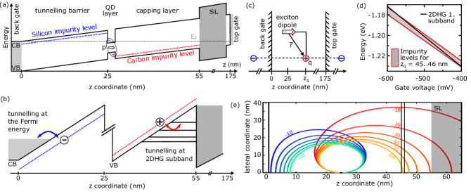
The self-assembled InGaAs QDs studied here were grown by molecular beam epitaxy (MBE) Leonard et al. (1993) with subsequent annealing, and have emission energies around eV. The QDs are embedded in a field-effect structure to allow deterministic control of the charge occupation of the dot Drexler et al. (1994). On the ‘back’ side, a nm thick GaAs tunnelling barrier separates the QDs from a heavily doped GaAs layer (thickness 20 nm, doping concentration ) which forms the back electrode. The ‘top’ side of the QD-layer is covered first by a nm thick GaAs capping layer, and then with an additional AlGaAs/GaAs SL of nm thickness. A nm NiCr layer was evaporated on top of the SL to form the second electrode.
The energy levels of individual QDs were investigated with photoluminescence (PL) Warburton et al. (2000) and differential transmission (DT) Alen et al. (2003) spectroscopy in a confocal microscope setup shown schematically in Figure 1(a). The sample had a QD density such that there were typically QDs in an area corresponding to a diffraction-limited focal spot of m diameter. Out of this small ensemble, individual QDs were spectrally selected for PL and DT measurements. By applying a gate voltage between the top gate and the back contact, the energy levels of a QD shift relative to the Fermi energy EF, allowing control over the number of electrons that occupy the dot Drexler et al. (1994). Figure 1(b) represents a typical QD PL charging diagram as a function of , showing the neutral exciton (X0) and the negatively charged exciton (X1-) emission resonances, respectively Warburton et al. (2000).
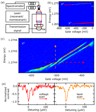
The neutral exciton transition was investigated in finer detail for a number of QDs using DT spectroscopy, with the polarization of the excitation laser chosen so as to excite just one of the two exchange-interaction split resonances Högele et al. (2004). Examples of DT spectra are shown in Figure 1(d). The calculated lifetime-limited linewidth of the X0 transition is eV, however the transition is further broadened due to charge fluctuations in the solid state matrix surrounding the QD Högele et al. (2004); Kuhlmann et al. (2013). For charge fluctuations that occur on a time scale much faster than the measurement integration times (typically 1 s), the resulting jitter in the QD resonance energy is observed as broadened linewidths in the range eV Högele et al. (2004); Kuhlmann et al. (2013).
For a significant fraction of QDs, the linear relationship between the exciton resonance energy and the applied gate voltage is interrupted by several distinct jumps. An example of this effect is apparent in Figure 1(c). The energy dispersion gradient is consistent across the X0 transition plateau, however there are discontinuities in energy observed at specific values of . With increasing , the transition energy jumps to lower values by an amount in the range of to eV. Such spectral discontinuities could be caused by similar environmental charge-fluctuations which give rise to exciton line-broadening. However, the spectral jumps studied here in more detail occur at specific gate voltages, and correspond to larger resonance-energy shifts in the QD transition. Recently, the work of Houel et al. Houel et al. (2012) attributed these spectral jumps to discrete charging of potential-traps located at the interface to the SL. Our analysis detailed below suggests the presence of additional potential-traps in the surrounding GaAs matrix.
III Modelling & Discussion
The exciton resonance energy of a QD is shifted by an electric field F through the quantum confined Stark effect:
| (1) |
where is the unperturbed exciton resonance energy, is the static dipole moment of the exciton transition, and is the polarizability Warburton et al. (2002). This relation quantifies how an applied electric field can be used to shift the exciton resonance deterministically, and also encompasses the mechanism through which charge fluctuations in the solid-state matrix surrounding the QD can perturb the resonance Houel et al. (2012).
An applied gate voltage generates an electric field , where is the distance between the layer and the top surface electrode, and V is the Schottky barrier potential Warburton et al. (2002). The axial polarizability along the growth direction has been measured for similar dots as eV/(kV/cm)2 Warburton et al. (2002). For the X0 transition, which occurs with in the range V, the effect of the axial polarizability is negligible compared to the much larger dipole contribution. Therefore, the magnitude of the dipole moment can be determined from the gradient of the X0 transition energy versus gate voltage as . Values of are typically (where is the elementary charge) for the strongly confining QDs surveyed in this work Warburton et al. (2002). In the QD plane, there is no permanent dipole moment, however the larger geometric extent of the dot in this direction implies a much larger lateral polarizability of the order of eV/(kV/cm)2 Gerardot et al. (2007). Therefore, charge fluctuations in the vicinity of a QD can perturb the exciton resonance by coupling to the permanent dipole moment in the -direction, or through the polarizability in the lateral plane.
The magnitude of the exciton resonance-energy shift caused by a single unit charge placed near the dot can be determined with a simple electrostatic model of the heterostructure depicted in Figure 2(c). A QD exciton is represented as a dipole oriented along the -axis, positioned between two electrodes. A charge-trapping site is located at an arbitrary distance from the dot, described by position vector r. Upon occupation of such a trapping potential, the change in the static electric field, , at the QD position is approximated as:
| (2) |
where is a unit charge equal to either , is the permittivity, is the dielectric constant of the surrounding GaAs matrix, and . The first term in the brackets arises from the impurity charge . The response of the freely-moving charges in the electrodes to the altered charge environment is included (to first order) as second and third terms in the form of image charges and , located behind the back gate and top electrode at and respectively [see Figure 2(c)].
Combining equations 1 and 2, the energy shift is obtained as a function of the position and parity of the added charge. As an example, Figure 2(e) shows the possible positions for added charges of either that would induce a step-change in exciton energy in the range of to eV, calculated for the QD1 in Figure 1 with nm. At large axial distances, the energy jumps could be caused by either a negative charge appearing below the dot, or a positive charge appearing above the dot, i.e. the observed charging events produce an electric field which opposes the externally-controlled field. In the lateral plane, the addition of either parity charge could induce such an energy shift. Aside from the magnitude of the energy jumps, their gate voltage dependence is also central to identifying the charge impurity location. Since the spectral jumps occur at specific gate voltages, this suggests that the individual trap sites are tuned through tunnel-resonances with charge reservoirs as is varied.
On the lower side of the dot, the most likely source of the electron-trapping sites are the silicon (Si) donor dopants. The back-gate consists of heavily Si-doped GaAs, and previous studies have shown that Si atoms diffuse during the growth process up to several tens of nm along the growth direction of the sample Kleemans et al. (2010). The energy level associated with the Si donor-electron lies meV below the GaAs conduction band edge Karasyuk et al. (1994), and the possible -controlled tunneling mechanism is a resonance with the Fermi level in the back gate [see Figure 2(b)]. A Si impurity site with in the range to nm would be consistent with the observed energy jumps occurring within the gate-voltage range of to mV. However, a change of at this location would induce a QD resonance-energy shift less than eV [see Figure 2(c)]. Such an energy shift is barely resolvable within the X0 linewidth, and indeed all the observed discontinuities investigated here have a larger change in energy. Therefore, we can exclude Si impurities as the origin for the observed spectral jumps.
In the region above the QD layer, carbon (C) atoms are the likely source of hole-trapping sites. There is inevitably a residual background C-doping in any MBE grown device, and the concentration is known to be on the order of cm-3 for our sample. The C acceptor atoms have an energy level meV above the valence band Heilman and Oelgart (1990). The -controlled tunneling resonance in this case involves a sub-band in the two-dimensional hole gas (2DHG) that forms at the interface to the AlGaAs/GaAs SL [depicted in Figure 2(b)]. The energy of the -subband in the 2DHG is given by Davies (1998):
| (3) |
where denotes the GaAs bandgap energy, is the valence band energy at the position of the 2DHG, is the Airy coefficient approximated by , and the effective mass Bouarissa and Aourag (1999). The carbon charge-trap energy as well as as a function of are shown in Figure 2(d), identifying resonance conditions in the range from to mV for a carbon atom with in the interval of nm. These -boundaries are depicted in Figure 2(e) to highlight the fact that a charge of located within this -slice can indeed induce energy shifts up to -60 eV. This location of the charge traps is well within in the GaAs capping layer and does not coincide with the interface to the SL Houel et al. (2012). Remarkably, however, our results are consistent with the observation that an increase of the separation between the QD layer and the SL is sufficient to inhibit spectral jumps in the plateau of X0 and favor the narrowing of the exciton resonance Houel et al. (2012). The displacement of the SL to larger values of implies a change in the resonance condition between the C-impurity level and the lowest 2DHG sub-band through in Equation 3 such that carbon impurity sites would effectively be depopulated at gate voltages characteristic of the X0 stability regime.
III.1 Impurity-site charging dynamics
The spectra of the X0 transition for the dots surveyed in the course of this work exhibited in general a more complex structure than would be expected from the simplistic model described above. The model explains the majority of spectral jumps, where the QD transition energy changes abruptly from one value to a lower one within a span of to mV. This overlap in gate voltage of the QD energies corresponding to charged and uncharged impurity states is indicative of the rate at which hole-tunnelling occurs between the impurity site and the 2DHG. A fast tunnelling process yields a small overlap in and vice versa, analogous to the overlaps observed in PL charging diagrams of QDs in samples with different thicknesses of the tunneling barrier between the QD and the Fermi reservoir and correspondingly different electron tunneling rates. In addition to the ‘sharp’ transitions in the charge state of the impurity site, we observe in our DT data instances where an impurity-site coexists in both charged and uncharged configurations over an extended gate voltage range of to mV. An example of such a coexistence can be seen in Figures 1(c) and 3(a) for between mV and mV. This behavior is inexplicable within the modelling framework developed above. A refined model should take into account not only resonant tunneling between the impurity site and the 2DHG, but also dynamic charge capture processes that occur in the presence of an optically generated charge reservoir Nguyen et al. (2013).
To qualitatively understand the impurity site charging dynamics, we adopt the rate-equation formalism of Ref. Nguyen et al. (2013) to determine the time averaged steady-state occupation of the impurity site as:
| (4) |
where and denote the rates at which a hole is captured in, or escapes from, the impurity trap respectively. In the simple case that was modelled above, when the impurity site is energetically higher than the subband of the 2DHG, and . Conversely, when the gate voltage is tuned such that the impurity site is below the lowest 2DHG subband, then , and . However, the capture rate can also be influenced by the excitation of charge carriers in the QD. Previous investigations have shown that the tunnelling rate of holes from a QD is significantly enhanced as it is tuned through resonances with energy levels in the 2DHG Seidl et al. (2005). It is possible therefore, for holes to tunnel from the QD to an level of the 2DHG, and then occupy the impurity-site before finally relaxing to the energetically favorable state of the 2DHG. These QD–DHG resonances effectively enhance such that it becomes comparable to (determined only by the valence band properties), and therefore it becomes feasible for the impurity-site to be partially occupied over an extended range, despite not being resonant itself with the 2DHG state. The QD–2DHG resonances observed in similar heterostructures were measured to occur over a range of 100 mV in Seidl et al. (2005), in agreement with the span in which we observe intermediate values of .
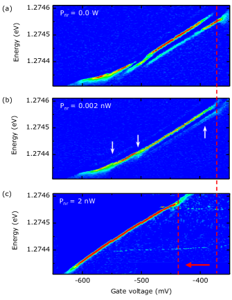
We can further dynamically perturb the charge environment of the system with the use of non-resonant optical excitation Houel et al. (2012). In addition to the resonant laser, the output of an 850 nm laser diode is directed onto the sample, which excites electron-hole pairs in the wetting layer. The effect of this additional charge-carrier generation on the QD charge sensing phenomena is two-fold, firstly altering the electrostatic response of the QD, and secondly directly influencing . The first of these effects is due to a build up of holes in the 2DEG, which are generated in the wetting layer, but due to the energy-gradient across the heterostructure, tend to relax into the 2DHG. This accumulation of positive charge at the interface to the SL has the effect of partially screening the dot from the externally applied field (causing the well known energy shift of the exciton plateau Smith et al. (2003)) as well as screening the QD from the impurity charge. Consequently the spectral jumps decrease monotonically in magnitude with increased non-resonant laser power (see Fig. 3). The effectiveness of the screening depends on the charge density of the 2DHG, and therefore is determined by the laser power. In the limit of high charge density, we can modify the electrostatic model to include the response of the 2DHG in the form of an additional mirror charge. With this modification, an energy jump in the QD spectra of 30 eV in the absence of non-resonant light is reduced to just 16 eV. In addition to this electrostatic shielding, the second effect of non-resonant excitation is the direct influence on Nguyen et al. (2013). The capture rate is increased with , and beyond a certain saturation power , despite the impurity trap not being energetically favorable compared to the level of the 2DHG. This dynamic saturation effect can be observed in Figure 3(c).
III.2 Single impurity sensed with multiple QDs
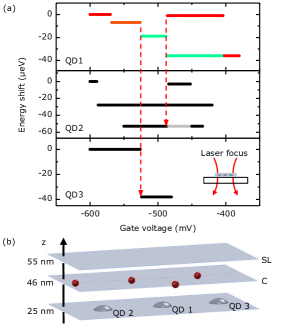
The transverse location of an impurity site cannot be pinpointed with just one QD sensor, however further constraints can be obtained by using multiple QDs within the impurity vicinity. The absorption spectra of three different QDs (labelled as QD1 to QD3) within a common focal spot (of 1 m in diameter) are shown in Figure 4(a), with the background linear Stark shift subtracted for clarity. It can be seen that there are concurrent spectral jumps occurring for two different QDs at the same gate voltage , which are likely caused by one single impurity. For the spectral-jumps which only occur in a single spectrum we assume the charge-trapping sites are too far away from the alternate dots for the spectral effects to be resolved.
As a specific example of the charge sensing capability, we determine the location of the impurity site that causes jumps in the spectra of QD1 and QD3. The -position of the charge impurity is calculated (using mV) as nm. The magnitude of the energy-jump in the QD1 spectrum is eV, while for QD2 the energy change is eV. The measured dipole moments for each of these dots ( and for QD1 and QD3, respectively) determine the transverse location of the impurity site as nm from QD1, and nm from QD3. If the relative locations of the QDs were known, there would be a unique solution for the location of the charge impurity. This concurrent sensing concept is depicted in Figure 4(b), showing the QDs linearly aligned, and a number of carbon impurity sites in the GaAs volume between the QD layer and the SL.
IV Conclusion
In summary, we have identified the cause of spectral jumps in the neutral exciton transitions of QDs as being due to charging of carbon impurity sites. Our results suggest these impurities are located in the semiconductor region surrounding the QD layer. This is further re-enforced by measuring the spectral signatures of the charge trapping concurrently for more than one QD. Despite the fact that the charge trapping sites are not themselves at the interface, our analysis suggests that moving the SL interface further from the dot layer would still improve the exciton resonance stability, by shifting the tunnel resonances to different gate voltages.
V Acknowledgments
We acknowledge funding by the Deutsche Forschungsgemeinschaft (SFB 631 and the German Excellence Initiative via the Nanosystems Initiative Munich, NIM) and support from the Center for NanoScience (CeNS).
References
- Imamoglu et al. (1999) A. Imamoğlu, D. D. Awschalom, G. Burkard, D. P. DiVincenzo, D. Loss, M. Sherwin, and A. Small, Phys. Rev. Lett. 83, 4204 (1999).
- Shields (2007) A. J. Shields, Nature Photonics 1, 215 (2007).
- Santori et al. (2002) C. Santori, D. Fattal, J. Vucković, G. S. Solomon, and Y. Yamamoto, Nature 419, 594 (2002).
- Gazzano et al. (2013) O. Gazzano, S. Michaelis de Vasconcellos, C. Arnold, A. Nowak, E. Galopin, I. Sagnes, L. Lanco, A. Lemaître, and P. Senellart, Nature Comm. 4, 1425 (2013).
- Michler et al. (2000) P. Michler, A. Kiraz, C. Becher, W. V. Schoenfeld, P. M. Petroff, L. Zhang, E. Hu, and A. Imamoğlu, Science 290, 2282 (2000).
- Stevenson et al. (2006) R. M. Stevenson, R. J. Young, P. Atkinson, K. Cooper, D. A. Ritchie, and A. J. Shields, Nature 439, 179 (2006).
- Atatüre et al. (2006) M. Atatüre, J. Dreiser, A. Badolato, A. Högele, K. Karrai, and A. Imamoğlu, Science 312, 551 (2006).
- Warburton (2013) R. J. Warburton, Nat. Mater. 12, 483 (2013).
- Gao et al. (2013) W. B. Gao, P. Fallahi, E. Togan, A. Delteil, Y. S. Chin, J. Miguel-Sanchez, and A. Imamoğlu, Nature Comm. 4, 2744 (2013).
- De Greve et al. (2012) K. De Greve, L. Yu, P. L. McMahon, J. S. Pelc, C. M. Natarajan, N. Y. Kim, E. Abe, S. Maier, C. Schneider, M. Kamp, et al., Nature 491, 421 (2012).
- Pfaff et al. (2014) W. Pfaff, B. Hensen, H. Bernien, S. B. van Dam, M. S. Blok, T. H. Taminiau, M. J. Tiggelman, R. N. Schouten, M. Markham, D. J. Twitchen, et al., Science 532 (2014).
- Högele et al. (2004) A. Högele, S. Seidl, M. Kroner, K. Karrai, R. J. Warburton, B. D. Gerardot, and P. M. Petroff, Phys. Rev. Lett. 93, 217401 (2004).
- Muller et al. (2007) A. Muller, E. B. Flagg, P. Bianucci, X. Y. Wang, D. G. Deppe, W. Ma, J. Zhang, G. J. Salamo, M. Xiao, and C. K. Shih, Phys. Rev. Lett. 99, 187402 (2007), ISSN 0031-9007.
- Vamivakas et al. (2009) A. N. Vamivakas, Y. Zhao, C. Lu, and M. Atatüre, Nature Phys. 5, 198 (2009), ISSN 1745-2473.
- Kuhlmann et al. (2013) A. V. Kuhlmann, J. Houel, A. Ludwig, L. Greuter, D. Reuter, A. D. Wieck, M. Poggio, and R. J. Warburton, Nature Phys. 9, 570 (2013).
- Nguyen et al. (2011) H. S. Nguyen, G. Sallen, C. Voisin, P. Roussignol, C. Diederichs, and G. Cassabois, Appl. Phys. Lett. 99, 261904 (2011).
- Matthiesen et al. (2012) C. Matthiesen, A. N. Vamivakas, and M. Atatüre, Phys. Rev. Lett. 108, 093602 (2012).
- Prechtel et al. (2013) J. H. Prechtel, A. V. Kuhlmann, J. Houel, L. Greuter, A. Ludwig, D. Reuter, A. D. Wieck, and R. J. Warburton, Phys. Rev. X 3, 041006 (2013).
- Houel et al. (2012) J. Houel, A. V. Kuhlmann, L. Greuter, F. Xue, M. Poggio, B. D. Gerardot, P. A. Dalgarno, A. Badolato, P. M. Petroff, A. Ludwig, et al., Phys. Rev. Lett. 108, 107401 (2012).
- Nguyen et al. (2013) H. S. Nguyen, G. Sallen, M. Abbarchi, R. Ferreira, C. Voisin, P. Roussignol, G. Cassabois, and C. Diederichs, Phys. Rev. B 87, 115305 (2013).
- Leonard et al. (1993) D. Leonard, M. Krishnamurthy, C. M. Reaves, S. P. Denbaars, and P. M. Petroff, Appl. Phys. Lett. 63, 3203 (1993).
- Drexler et al. (1994) H. Drexler, D. Leonard, W. Hansen, J. P. Kotthaus, and P. M. Petroff, Phys. Rev. Lett. 73, 2252 (1994).
- Warburton et al. (2000) R. J. Warburton, C. Schaflein, D. Haft, F. Bickel, A. Lorke, K. Karrai, J. M. Garcia, W. Schoenfeld, and P. M. Petroff, Nature 405, 926 (2000).
- Alen et al. (2003) B. Alen, F. Bickel, K. Karrai, R. J. Warburton, and P. M. Petroff, Appl. Phys. Lett. 83, 2235 (2003).
- Warburton et al. (2002) R. J. Warburton, C. Schulhauser, D. Haft, C. Schäflein, K. Karrai, J. M. Garcia, W. Schoenfeld, and P. M. Petroff, Phys. Rev. B 65, 113303 (2002).
- Gerardot et al. (2007) B. D. Gerardot, S. Seidl, P. A. Dalgarno, R. J. Warburton, D. Granados, J. M. Garcia, K. Kowalik, O. Krebs, K. Karrai, A. Badolato, et al., Appl. Phys. Lett. 90, 041101 (2007).
- Kleemans et al. (2010) N. A. J. M. Kleemans, J. van Bree, A. O. Govorov, J. G. Keizer, G. J. Hamhuis, R. Nötzel, A. Y. Silov, and P. M. Koenraad, Nature Phys. 6, 534 (2010).
- Karasyuk et al. (1994) V. A. Karasyuk, D. G. S. Beckett, M. K. Nissen, A. Villemaire, T. W. Steiner, and M. L. W. Thewalt, Phys. Rev. B 49, 16381 (1994).
- Heilman and Oelgart (1990) R. Heilman and G. Oelgart, Semiconductor Science and Technology 5, 1040 (1990).
- Davies (1998) J. H. Davies, The physics of low-dimensional semiconductors (Cambridge University Press, 1998).
- Bouarissa and Aourag (1999) N. Bouarissa and H. Aourag, Infrared Phys.Technol. 40, 343 (1999).
- Seidl et al. (2005) S. Seidl, M. Kroner, P. Dalgarno, A. Högele, J. Smith, M. Ediger, B. Gerardot, J. Garcia, P. Petroff, K. Karrai, et al., Phys. Rev. B 72, 195339 (2005).
- Smith et al. (2003) J. M. Smith, P. A. Dalgarno, B. Urbaszek, E. J. McGhee, G. S. Buller, G. J. Nott, R. J. Warburton, J. M. Garcia, W. Schoenfeld, and P. M. Petroff, Applied Physics Letters 82, 3761 (2003).