Electronic Structure of Epitaxial Single-Layer MoS2
Abstract
The electronic structure of epitaxial single-layer MoS2 on Au(111) is investigated by angle-resolved photoemission spectroscopy. Pristine and potassium-doped layers are studied in order to gain access to the conduction band. The potassium-doped layer is found to have a (1.390.05) eV direct band gap at with the valence band top at having a significantly higher binding energy than at . The moiré superstructure of the epitaxial system does not lead to the presence of observable replica bands or minigaps. The degeneracy of the upper valence band at is found to be lifted by the spin-orbit interaction, leading to a splitting of (1454) meV. This splitting is anisotropic and in excellent agreement with recent calculations. Finally, it is shown that the strength of the potassium doping is -dependent, leading to the possibility of band structure engineering in single-layers of transition metal dichalcogenides.
pacs:
73.22.-f,73.20.At,79.60.-iSoon after the first isolation of graphene Novoselov et al. (2004); Novoselov et al. (2005a); Zhang et al. (2005), it became clear that other layered materials could also be thinned down to a single layer using the same methods, and that such layers may have interesting properties Novoselov et al. (2005b). Particular focus has been on MoS2 Mak et al. (2010); Splendiani et al. (2010); Cao et al. (2012); Radisavljevic et al. (2011); Zeng et al. (2012); Xiao et al. (2012), a material that had been grown in single layers and used in catalysis even before the advent of graphene Topsøe et al. (1996); Helveg et al. (2000); Lauritsen et al. (2003); Jaramillo et al. (2007). Single-layer (SL) MoS2 has indeed been shown to have a number of intriguing properties. To name but a few, SL MoS2 has a direct band gap in contrast to the bulk Bollinger et al. (2001) and correspondingly different optical properties Mak et al. (2010); Splendiani et al. (2010). Having the conduction band minimum at the point of the Brillouin zone (BZ) opens interesting possibilities for new valley and spin-valley physics Cao et al. (2012); Zeng et al. (2012); Xiao et al. (2012). It is also possible to construct transistors based on SL MoS2 with the advantage of a high on/off ratio compared to (bilayer) graphene-based devices Radisavljevic et al. (2011).
Instead of obtaining SL MoS2 by micro mechanical exfoliation, high-quality layers can be grown on different substrates, enabling a new avenue for fundamental investigations of this material. While the growth of nano scale SL MoS2 clusters is particularly well established Helveg et al. (2000); Lauritsen et al. (2007), it has recently become possible to grow large area epitaxial SL MoS2 Sørensen et al. (2014). Similar to many epitaxial graphene systems Berger et al. (2004); N’Diaye et al. (2008), the structure of SL MoS2 shows a strong moiré superlattice due to the lattice mismatch with the underlying Au(111) Sørensen et al. (2014). In this work, we exploit the very high quality and large areas obtainable for epitaxial SL MoS2 to study its electronic structure by angle-resolved photoemission spectroscopy (ARPES). This provides a detailed picture of the new effects arising from quantum confinement, breaking of the bulk inversion symmetry, the role of spin-orbit coupling, as well as the effect of the underlying Au(111) and the moiré structure.
Epitaxial SL MoS2 has been grown on Au(111) by methods described elsewhere Sørensen et al. (2014). Actually, the total MoS2 coverage used here was kept somewhat below one monolayer at ML in order to avoid the growth of 2 ML islands that were found to be detectable in ARPES. The epitaxial SL MoS2 samples are stable in air and could thus be removed from the dedicated growth chamber, transported to the SGM-3 end station on the synchrotron radiation source ASTRID2 Hoffmann et al. (2004) and cleaned via mild annealing to 500 K, a procedure that has been verified to yield atomically clean surfaces by scanning tunnelling microscopy (STM). ARPES data were collected at 80 K with an energy and angular resolution better than 20 meV and 0.2∘, respectively. All measurements presented here were performed with a photon energy of 49 eV. Even though the band structure of SL MoS2 is easily distinguished from the photoemission features from the underlying Au(111), photon energy scans were performed to confirm the lack of dispersion of the SL MoS2 bands.
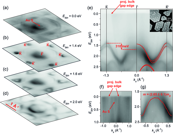
Figure 1 gives an overview of the epitaxial SL MoS2 band structure. The constant binding energy cuts in Fig. 1(a-d) reveal both Au(111) and SL MoS2 features. The Au(111)-related states are best identified near the Fermi energy due to the lack of SL MoS2 states there. At higher binding energies, maxima in the upper valence band (VB) states of SL MoS2 are observed, both at the as well as at the points. These features are also seen in the measured dispersion shown in Fig. 1(e). While the states near are very distinct and sharp, those near are rather broad. This is ascribed to the different interaction with the substrate and the orbital character of the states. The upper VB near falls into a projected band gap of the Au(111) electronic structure Takeuchi et al. (1991) and can therefore not interact with the bulk states. Indeed, the presence of this gap is even visible in the data of Fig. 1(e) as a reduction of background intensity between the Fermi energy and 2.2 eV binding energy around . Moreover, the upper VB near is derived from in-plane d- and p-orbitals orbitals Zhu et al. (2011); Cappelluti et al. (2013) and thus a weak adsorbate-substrate interaction is expected. The upper VB states near , on the other hand, fall within the continuum of projected bulk states Takeuchi et al. (1991) and are derived from out-of-plane orbitals Zhu et al. (2011); Cappelluti et al. (2013). For these states a stronger adsorbate-substrate interaction can be expected and this can explain the broadening of the band.
Such an increased interaction is also supported by a comparison of the measured dispersion and the density functional theory band structure for free-standing SL MoS2 by Zhu et al. Zhu et al. (2011). In Fig. 1(e) this calculation is superimposed on the data and aligned at the valence band maximum (VBM) at . In the calculation, the upper VB maxima at and are found at nearly the same binding energy. This is also the case for calculations that include many-body effects Cheiwchanchamnangij and Lambrecht (2012) and in ARPES results from exfoliated SL MoS2 Jin et al. (2013). Our data, in contrast, show a distortion of the upper VB with the measured maximum at being 0.31 eV lower than at . The distortion has only a small effect on the effective mass near . A fit to a hole-like parabola (see Fig. 1(g)) gives an effective hole mass of (2.70.1) times the free electron mass , in agreement with the calculation for SL MoS2 (2.8 ) Peelaers and Van de Walle (2012) and the result for exfoliated SL MoS2 ((2.40.3) ) Jin et al. (2013), but much higher than the calculated bulk value (0.62 ) Peelaers and Van de Walle (2012).
Figure 1(f) shows a magnification of the dispersion around near the Fermi energy. Here the diffuse background intensity is higher in the projected bulk state continuum of Au(111) than in the projected band gaps. The bulk band structure gap opening around the bulk L point leads to a small projected band gap around Takeuchi et al. (1991) that is also observed here. Within this gap, we even find a diffuse intensity that is assigned to the well-known surface state on Au(111) Reinert et al. (2001). The corresponding disc of intensity is also visible at the Fermi energy cut in Fig. 1(a). The surface state’s presence under SL MoS2 and also under MoS2 films completely covering the surface (not shown) suggest that the adsorbate-substrate interaction is predominantly of van der Waals character, as in the case of graphene on Ir(111) where a similar phenomenon is observed Varykhalov et al. (2012).
Another expected consequence of the SL MoS2-substrate interaction would be a manifestation of the pronounced moiré in the electronic structure. A scanning tunnelling microscopy image of the moiré is shown in the inset of Fig. 1(e). A similar moiré has pronounced consequences for the electronic structure of epitaxial graphene, leading to the presence of replica bands and mini-gaps in the Dirac cone Bostwick et al. (2007); Pletikosic et al. (2009). Here, such replicas would be expected at a distance of Å-1 from the main features. We should easily be able to resolve such features, especially for the sharp bands near , but we find them absent from the data, suggesting that the electronic structure of SL MoS2 is hardly affected by the moiré. We ascribe the difference to graphene to the different character of the states near : In graphene, the buckling of the layer directly affects the local interaction of the out-of-plane orbitals with the substrate. In MoS2, on the other hand, the bands have a mix of Mo , and S , character and are thus totally in-plane. Their local interaction with the substrate can be expected to be less affected by the buckling.
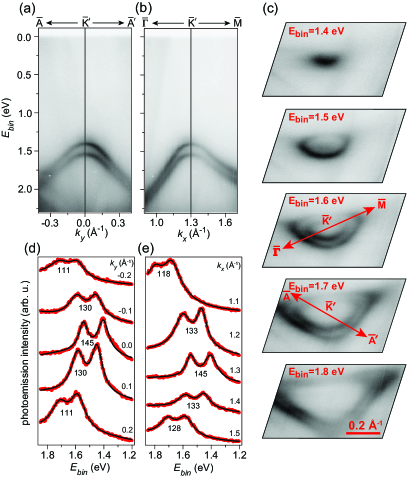
A remarkable effect is the strong spin-orbit splitting of the upper VB near , shown in greater detail in Fig. 2. Note that the splitting in SL MoS2 is a genuine lifting of the spin-degeneracy and different from the splitting in the inversion-symmetric bulk material, where it is a combination of layer interaction and spin-orbit coupling and does not remove the spin degeneracy Cheiwchanchamnangij and Lambrecht (2012). An equivalent splitting has been observed in ARPES from ML MoSe2 grown on epitaxial graphene Zhang et al. (2014) but it has so far remained unresolved for exfoliated SL MoS2 Jin et al. (2013). The size of the splitting can be determined from a fit of the energy distribution curves (EDCs) obtained from the data in Fig. 2(a,b) and shown in Fig. 2(d,e). The strongest splitting at is found to be (1454) meV. This is somewhat bigger than the value of meV obtained by triply resonant Raman scattering Sun et al. (2013) and, as expected, smaller than the ARPES result for ML MoSe2 of 180 meV. It is in excellent agreement with the theoretical prediction of 148 meV from density functional theory Zhu et al. (2011) and 146 meV from GW calculations Cheiwchanchamnangij and Lambrecht (2012). The anisotropy of the splitting away from that gives rise to a triangular warping of the constant energy contours in Fig. 2(c) also agrees with the theoretical prediction Zhu et al. (2011).
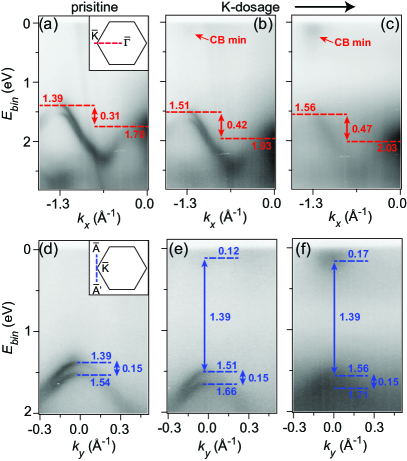
SL MoS2 is expected to be a semiconductor with a direct band gap at , in contrast to the bulk that has an indirect band gap Bollinger et al. (2001); Mak et al. (2010); Splendiani et al. (2010). Access to the conduction band minimum (CBM) of the SL MoS2 in ARPES is possible by doping with potassium. This is illustrated in Fig. 3 which shows a series of scans along the and directions of the BZ for the clean surface and an increasing exposures to potassium. Overall, the expected strong electron doping is indeed observed: For a small potassium dose, all bands are shifted to higher binding energies and a weak photoemission intensity due to the conduction band minimum at becomes observable (Fig. 3(b) and (e)). As the doping is increased, the CBM becomes populated, demonstrating the direct band gap of the material, as the VBM is also at (Fig. 3(c) and (f)). The CBM is found to be rather broad, in contrast to the VBM at , consistent with the out-of-plane character of these states Zhu et al. (2011); Cappelluti et al. (2013). We determine the gap energy to be (1.390.05) eV, substantially smaller than the value of 1.88 eV determined by photoluminescence Mak et al. (2010).
Upon closer inspection, it becomes clear that potassium adsorption does not give rise to a simple rigid shift of the band structure to higher binding energies: While the VBM at shifts by 1.39 eV - 1.56 eV = -0.17 eV from the clean sample to the highly potassium-dosed situation, the maximum at shifts by 1.70 eV - 2.03 eV = -0.33 eV, such that the upper VB is severely distorted upon doping. This is again ascribed to the different orbital character near the high symmetry points, with the states at being likely to show a stronger adsorbate-substrate interaction. Note that the same effect might also contribute to the small observed gap: The CBM states have a similar symmetry as the upper VB states at and the observed gap for the potassium-dosed case is thus likely to be smaller than the gap of the pristine epitaxial SL MoS2.
In conclusion, we have studied the electronic structure of epitaxial single-layer MoS2 on Au(111). We find this to give rise to sharp bands, in particular for the VBM near the point and these bands are minimally affected by the presence of the substrate or moiré. This is very different from the band in epitaxial graphene and we ascribe this to the different orbital character of the bands (in-plane for MoS2 versus out-of-plane for graphene). We directly observe the strong spin splitting of the upper VB and the size of this is in excellent agreement with theoretical predictions. Upon doping the layer with potassium, we are able to determine the band gap and find that the doping-induced shifts in energy are strongly dependent on the orbital character of the bands and hence . This opens interesting possibilities to intentionally tune the band structure of SL MoS2 and similar materials. The effect also needs to be taken into account when placing SL MoS2 between other materials or when doping it by an electric field.
We gratefully acknowledge financial support from the VILLUM foundation, The Danish Council for Independent Research, the Lundbeck Foundation,The Danish Strategic Research Council (CAT-C) and Haldor Topsøe A/S.
References
- Novoselov et al. (2004) K. S. Novoselov, A. K. Geim, S. V. Morozov, D. Jiang, Y. Zhang, S. V. Dubonos, I. V. Grigorieva, and A. A. Firsov, Science 306, 666 (2004).
- Novoselov et al. (2005a) K. S. Novoselov, A. K. Geim, S. V. Morozov, D. Jiang, M. I. Katsnelson, I. V. Grigorieva, S. V. Dubonos, and A. A. Firsov, Nature 438, 197 (2005a).
- Zhang et al. (2005) Y. B. Zhang, Y. W. Tan, H. L. Stormer, and P. Kim, Nature 438, 201 (2005).
- Novoselov et al. (2005b) K. S. Novoselov, D. Jiang, F. Schedin, T. J. Booth, V. V. Khotkevich, S. V. Morozov, and A. K. Geim, Proceedings of the National Academy of Sciences of the United States of America 102, 10451 (2005b).
- Mak et al. (2010) K. F. Mak, C. Lee, J. Hone, J. Shan, and T. F. Heinz, Phys. Rev. Lett. 105, 136805 (2010).
- Splendiani et al. (2010) A. Splendiani, L. Sun, Y. Zhang, T. Li, J. Kim, C.-Y. Chim, G. Galli, and F. Wang, Nano Letters 10, 1271 (2010).
- Cao et al. (2012) T. Cao, G. Wang, W. Han, H. Ye, C. Zhu, J. Shi, Q. Niu, P. Tan, E. Wang, B. Liu, et al., Nature Communications 3, 887 (2012).
- Radisavljevic et al. (2011) B. Radisavljevic, A. Radenovic, J. Brivio, V. Giacometti, and A. Kis, Nature Nanotechnology 6, 147 (2011).
- Zeng et al. (2012) H. Zeng, J. Dai, W. Yao, D. Xiao, and X. Cui, Nature Nanotechnology 7, 490 (2012).
- Xiao et al. (2012) D. Xiao, G.-B. Liu, W. Feng, X. Xu, and W. Yao, Phys. Rev. Lett. 108, 196802 (2012).
- Topsøe et al. (1996) H. Topsøe, B. S. Clausen, and F. E. Massoth, Hydrotreating Catalysis, vol. 11 of Catalysis - Science and Technology (Springer Verlag, Berlin-Heidelberg, 1996).
- Helveg et al. (2000) S. Helveg, J. V. Lauritsen, E. Lægsgaard, I. Stensgaard, J. K. Nørskov, B. S. Clausen, H. Topsøe, and F. Besenbacher, Phys. Rev. Lett. 84, 951 (2000).
- Lauritsen et al. (2003) J. Lauritsen, M. Nyberg, R. Vang, M. Bollinger, B. Clausen, H. Topsoe, K. Jacobsen, E. Laegsgaard, J. Norskov, and F. Besenbacher, Nanotechnology 14, 385 (2003).
- Jaramillo et al. (2007) T. F. Jaramillo, K. P. Jorgensen, J. Bonde, J. H. Nielsen, S. Horch, and I. Chorkendorff, Science 317, 100 (2007).
- Bollinger et al. (2001) M. V. Bollinger, J. V. Lauritsen, K. W. Jacobsen, J. K. Nørskov, S. Helveg, and F. Besenbacher, Physical Review Letters 87, 196803 (2001).
- Lauritsen et al. (2007) J. V. Lauritsen, J. Kibsgaard, S. Helveg, H. Topsoe, B. S. Clausen, E. Laegsgaard, and F. Besenbacher, Nature Nanotechnology 2, 53 (2007).
- Sørensen et al. (2014) S. G. Sørensen, H. G. Füchtbauer, A. K. Tuxen, A. S. Walton, and J. V. Lauritsen, ACS Nano 8, 6788 (2014).
- Berger et al. (2004) C. Berger, Z. Song, T. Li, X. Li, A. Y. Ogbazghi, R. Feng, Z. Dai, A. N. Marchenkov, E. H. Conrad, P. N. First, et al., The Journal of Physical Chemistry B 108, 19912 (2004).
- N’Diaye et al. (2008) A. T. N’Diaye, J. Coraux, T. N. Plasa, C. Busse, and T. Michely, New Journal of Physics 10, 043033 (2008).
- Hoffmann et al. (2004) S. V. Hoffmann, C. Søndergaard, C. Schultz, Z. Li, and P. Hofmann, Nuclear Instruments and Methods in Physics Research, A 523, 441 (2004).
- Zhu et al. (2011) Z. Y. Zhu, Y. C. Cheng, and U. Schwingenschlögl, Phys. Rev. B 84, 153402 (2011).
- Takeuchi et al. (1991) N. Takeuchi, C. T. Chan, and K. M. Ho, Phys. Rev. B 43, 13899 (1991).
- Cappelluti et al. (2013) E. Cappelluti, R. Roldán, J. A. Silva-Guillén, P. Ordejón, and F. Guinea, Phys. Rev. B 88, 075409 (2013).
- Cheiwchanchamnangij and Lambrecht (2012) T. Cheiwchanchamnangij and W. R. L. Lambrecht, Phys. Rev. B 85, 205302 (2012).
- Jin et al. (2013) W. Jin, P.-C. Yeh, N. Zaki, D. Zhang, J. T. Sadowski, A. Al-Mahboob, A. M. van der Zande, D. A. Chenet, J. I. Dadap, I. P. Herman, et al., Phys. Rev. Lett. 111, 106801 (2013).
- Peelaers and Van de Walle (2012) H. Peelaers and C. G. Van de Walle, Phys. Rev. B 86, 241401 (2012).
- Reinert et al. (2001) F. Reinert, G. Nicolay, S. Schmidt, D. Ehm, and S. Hüfner, Physical Review B 63, 115415 (2001).
- Varykhalov et al. (2012) A. Varykhalov, D. Marchenko, M. R. Scholz, E. D. L. Rienks, T. K. Kim, G. Bihlmayer, J. Sánchez-Barriga, and O. Rader, Phys. Rev. Lett. 108, 066804 (2012).
- Bostwick et al. (2007) A. Bostwick, T. Ohta, T. Seyller, K. Horn, and E. Rotenberg, Nature Physics 3, 36 (2007).
- Pletikosic et al. (2009) I. Pletikosic, M. Kralj, P. Pervan, R. Brako, J. Coraux, A. T. N’Diaye, C. Busse, and T. Michely, Physical Review Letters 102, 056808 (2009).
- Zhang et al. (2014) Y. Zhang, T.-R. Chang, B. Zhou, Y.-T. Cui, H. Yan, Z. Liu, F. Schmitt, J. Lee, R. Moore, Y. Chen, et al., Nature Nanotechnology 9, 111 (2014).
- Sun et al. (2013) L. Sun, J. Yan, D. Zhan, L. Liu, H. Hu, H. Li, B. K. Tay, J.-L. Kuo, C.-C. Huang, D. W. Hewak, et al., Phys. Rev. Lett. 111, 126801 (2013).