Strong coupling between a permalloy ferromagnetic contact and a helical edge channel in a narrow HgTe quantum well
Abstract
We experimentally investigate spin-polarized electron transport between a permalloy ferromagnet and the edge of a two-dimensional electron system with band inversion, realized in a narrow, 8 nm wide HgTe quantum well. In zero magnetic field, we observe strong asymmetry of the edge potential distribution with respect to the ferromagnetic ground lead. This result indicates, that the helical edge channel, specific for the structures with band inversion even at the conductive bulk, is strongly coupled to the ferromagnetic side contact, possibly due to the effects of proximity magnetization. It allows selective and spin-sensitive contacting of helical edge states.
pacs:
73.40.Qv 71.30.+hI Introduction
Recently, there is a strong interest in two-dimensional semiconductor systems with an inverted band structure, like narrow HgTe quantum wells. This interest is mostly connected with the quantum spin-Hall (QSH) effect regime konig ; kvon . Similarly to the conventional quantum Hall (QH) effect in high magnetic fields buttiker , QSH regime is characterized molenkamp_nonlocal ; kvon_nonlocal by presence of two spin-resolved, current-carrying helical edge states pankratov ; zhang1 ; kane ; zhang2 even in zero magnetic field. The helical QSH edge states are regarded to be suitable for different applications like quantum computing and cryptography.
Experimental investigations of helical QSH edge states are mostly based on charge transport along the edge, which has been detected in local and non-local resistance measurements konig ; kvon ; molenkamp_nonlocal ; kvon_nonlocal and by a direct visualization technique imaging . In the last case, the edge current has even been demonstrated to coexist with the conductive bulk imaging , which is also possible from theoretical considerations pankratov ; volkov . Despite the initial idea of a topological protection konig ; zhang1 ; kane ; zhang2 , backscattering appears at macroscopic distances kvon ; kvon_nonlocal , possibly due to the allowed two-particle process mirlin or to the electron puddles glazman .
It is clear that for possible applications, it is necessary to develop a technique of selective contacting of these edge states. A possible variant is to use spin effects: QSH edge transport is supposed to be essentially spin-dependent pankratov ; zhang1 ; kane ; zhang2 even in zero magnetic field. Strong coupling between the spin-resolved helical edge states and a ferromagnet can also be anticipated from theoretical considerations qi ; lunde .
Here, we experimentally investigate spin-polarized electron transport between a permalloy ferromagnet and the edge of a two-dimensional electron system with band inversion, realized in a narrow, 8 nm wide HgTe quantum well. In zero magnetic field, we observe strong asymmetry of the edge potential distribution with respect to the ferromagnetic ground lead. This result indicates that the helical edge channel, specific for the structures with band inversion even at the conductive bulk, is strongly coupled to the ferromagnetic side contact, possibly due to the effects of proximity magnetization. It allows selective and spin-sensitive contacting of helical edge states.
II Samples and technique
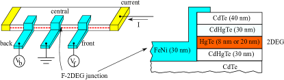
Our quantum wells are grown by molecular beam epitaxy on GaAs substrate with [013] surface orientations. The layer sequence is shown in Fig. 1, a detailed description can be found elsewhere growth1 ; growth2 . Our wells are characterized by band inversion kvon ; kvon_nonlocal , because the wells’ width nm is above the critical value 6.3 nm. They contain a 2DEG with the electron density of cm-2, as obtained from standard magnetoresistance measurements. The 2DEG mobility at 4K equals to cm2/Vs. For samples with higher nm , a 2D system in the quantum well represents an indirect 2D semimetal kvon_s1 ; kvon_s2 . Both electrons and holes contribute to transport in this case. The carriers’ concentrations are low enough, about cm-2 and cm-2 for electrons and holes, respectively. Electrons’ low-temperature mobility is about cm2/Vs, because the holes (with lower cm2/Vs mobility) provide efficient disorder screening kvon_scat .
Our principal idea is to use side contact to the 2DEG edge at the mesa step feinas ; nbnhgte ; nbsemi . Indeed, the usual procedure with annealed In contacts is not selective with respect to the edge state transport. Annealed In provides high-quality Ohmic contact primary to the bulk 2DEG. Thus, despite the edge current is allowed pankratov ; volkov to coexist with the conductive bulk imaging , edge state transport can only be investigated near the charge-neutrality point konig ; kvon ; molenkamp_nonlocal ; kvon_nonlocal . In contrast, without annealing procedure, the side contact is coupled to the 2DEG edge at the mesa step, because the CdTe layer on the top of the structure is a high-quality insulator at low temperatures.
A sample sketch is presented in Fig. 1. The 100 m wide mesa is formed by dry etching (200 nm deep) in Ar plasma. We fabricate F-2DEG junctions by using rf sputtering to deposit 50 nm thick ferromagnetic permalloy stripes at the mesa step, with low (2-3 m) overlap. The stripes are formed by lift-off technique, and the surface is mildly cleaned by Ar plasma before sputtering. To avoid any 2DEG degradation, the sample is not heated during the sputtering process. The source-drain contacts (yellow in Fig. 1) are obtained by thermal evaporation of 100 nm thick Au, as well as the normal Au-2DEG side junctions for reference samples.
We study electron transport across one particular F-2DEG junction in a three-point technique, see Fig. 1: the central ferromagnetic electrode is grounded; a current is applied between it and one of the normal (source or drain) contacts; two other permalloy contacts (front and back) trace the 2DEG potential to both sides of the grounded junction, and , respectively.
We sweep the dc current and measure voltages in a mV range by a dc electrometer, the resulting characteristics are presented in Fig. 2,3. To obtain characteristics in Fig. 5, this dc current is additionally modulated by a low ac component (0.01 nA, 2 Hz). We measure the ac () component of the 2DEG potential by using a lock-in with a 100 M input preamplifier. We have checked, that the lock-in signal is independent of the modulation frequency in the range 1 Hz – 6 Hz, which is defined by applied ac filters.

The measurements are performed at a temperature of 30 mK. To realize a spin-polarized transport, the permalloy stripes are initially pre-magnetized in the 2DEG plane feinas . The sample is placed within a superconducting solenoid, so the initial in-plane magnetization can be changed by introducing relatively high (above 1 T) external magnetic field. The field is switched to zero afterward, so the measurements are performed in zero magnetic field.
Qualitatively similar results were obtained from different samples in several cooling cycles. We study several samples of the type A (from both 8-nm and 20-nm HgTe quantum wells), which are depicted in Fig. 1, and one of the type B, which is additionally covered by a metallic Al gate. The gate covers all the sample (bulk 2DEG, mesa edges, all F-2DEG junctions), except for the normal Ohmic contacts. To avoid gate leakage, Al gate is placed over a 350 nm thick dielectric (guanine) layer. We check that there is no noticeable gate leakage through the dielectric at V dc gate bias. As a reference, we use a sample with Au (normal) side junctions instead of the permalloy ones.
III Experimental results
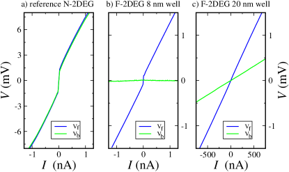
Examples of characteristics are presented in Fig. 2 for transport across a single normal N-2DEG (a) or ferromagnetic F-2DEG (b,c) junction.
In a three-point technique, the measured potential reflects in-series connected resistances of the grounded contact and the 2DEG. This technique is especially convenient if the former term is dominant. In this case, the 2DEG is equipotential, so the measured three-point curve is independent of the particular positions of the current/voltage probes.
This is exactly that we have for the reference normal Au-2DEG junction, see Fig. 2 (a). curves coincide well for both potential probes and . Thus, the measured three-point curves in Fig. 2 (a) reflect the behavior of the (grounded) Au-2DEG interface. These curves are obviously non-linear and are characterized by a high resistance (about 10 M) in Fig. 2 (a). The low-current resistive region with two kinks at about mV indicates a significant potential barrier (depletion region shklovskii ; image02 ) at the 2DEG edge. Similar high-resistive junctions we have obtained for other non-magnetic materials like sputtered Nb and NbN nbnhgte .
Our most prominent experimental result is demonstrated in Fig. 2 (b). If we ground the permalloy ferromagnetic side contact to the 8 nm HgTe quantum well, as depicted in Fig. 1, the measured potential is strongly asymmetric. We obtain a significant signal , i.e. for the voltage probe placed between the current and ground ones, but is always zero. We observe the same behavior for both current polarities and for two different current probes in Fig. 1, so the asymmetry between and is not connected with any absolute direction in the sample. This asymmetry is only determined by the mutual positions of the current and voltage contacts with respect to the grounded ferromagnetic lead. Identical behavior is obtained for different ferromagnetic contacts and different 8 nm well samples. We wish to emphasize that the behavior, depicted in Fig. 2 (b), is very unusual and is in a high contrast to the standard three-point resistance of a reference Au contact in Fig. 2 (a).
The asymmetry can not originate from bulk 2DEG contribution to the measured potential: different signals would require the bulk 2DEG resistance to exceed strongly the F-2DEG interface contribution. Because of high-resistive curves (about 1 M corresponding resistance) in Fig. 2 (b), this is inconsistent with the metallic bulk conductivity (below 1 k) at cm-2 electron concentration in our samples.
To verify this conclusion experimentally, similar measurements are performed for a 20 nm width HgTe quantum well, see Fig. 2 (c). and are also different in this case, however, they are of the same order of magnitude: we do not observe in this case. Both experimental curves correspond to about 1 k resistance, which is comparable with the bulk values. In other words, Fig. 2 (c) experimentally demonstrates the typical effect of bulk current contribution to a three-point signal in the case of low F-2DEG interface resistance.
The only difference between 8 nm and 20 nm HgTe quantum wells is the conductive helical edge channel in the former case molenkamp_nonlocal ; kvon_nonlocal . From the continuous evolution of the edge current when the system is driven away from the charge-neutral regime, demonstrated in Ref. imaging, by a direct visualization experiment, one can reasonably suppose that the edge current is still carried by helical spin-resolved edge states even at the conductive bulk 2DEG. It requires low coupling between the edge states and the bulk, possibly because of the formation of a depletion region where the edge channel is laterally localized imaging . The depletion region of finite width is often present at the 2DEG edge due to electrostatic effects shklovskii ; image02 . This depletion region is also confirmed in our experiment by the zero for any distance to the potential probe in Fig. 2 (b).
Since the conductive channel is present at the edge of a 8 nm HgTe quantum well, the perfect ( for any current ) asymmetry of the edge potential , observed in Fig. 2 (b), indicates that the grounded ferromagnetic side electrode is perfectly coupled to this channel.
We verify the statement of ideal coupling of the ferromagnetic lead to the edge current by standard two-point characterization, see Fig. 3. It can be seen in the figure, that the two-point F-2DEG-F curve, measured between two neighbor ferromagnetic contacts, coincides well with the three-point potential from Fig. 2 (b), so the interface contributions are negligible. In contrast, the experimental Au-2DEG-Au curve in Fig. 3 (a) corresponds to a roughly two times higher resistance than three-point potentials from Fig. 2 (a), so it mostly reflects the resistance of two resistive Au-2DEG interfaces.
IV Discussion
We should conclude that only a ferromagnetic permalloy side contact is strongly coupled to the conductive helical edge channel in zero magnetic field: (i) the perfect ( for any current ) asymmetry of the edge potential , see Fig. 2 (b), is only observed for the 8 nm quantum well; (ii) the coincidence between the two-point F-2DEG-F curve with the three-point potential, see Fig. 3 (b), directly indicates negligible F-2DEG interface contributions.
If the transport current is concentrated at the edge, it is flowing along the shortest edge to the ground lead and there should be no current flowing near the potential probe , so for any current . The potential in Fig. 2 (b) reflects therefore solely the resistance of the edge channel between two ferromagnetic contacts. It corresponds to about 1 M resistance, which is also well known for a transport along the helical current-carrying states at macroscopic distances kvon_nonlocal . It is worth to mention, that this 1 M resistance is still much smaller than the resistance for transport through the edge depletion region to the bulk (cp. with Fig. 2 (a)), so the edge channel is still decoupled from the bulk even at macroscopic distances.
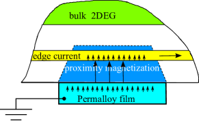
This strong coupling is not defined by chemical composition of the metallic film or the fabrication technique: the sputtered permalloy film contacts the 20 nm HgTe quantum well similarly to other non-magnetic materials. There should be a specific magnetic (spin-dependent) process, which couples the spin-polarized ferromagnetic side contact and the one-dimensional helical channel at the edge of a 2DEG with band inversion: a proximity magnetization locally aligns qi ; lunde the spins of two helical edge states in the vicinity of the ferromagnetic contact. The spin-polarized electron flow from the ferromagnetic contact can be easily injected to the helical state with corresponding spin projection. The depletion at the interface decouples the bulk 2DEG and makes the helical edge mode even more important. Farther transport along the sample edge is diffusive at at macroscopic distances kvon ; kvon_nonlocal , because of allowed backscattering mirlin ; glazman , so the injected electrons are flowing along the shortest edge to the ground lead. The coupling is independent of the magnetization direction, as we observe in the experiment, because it is the contact magnetization that defines the spin alignment direction, see Fig. 4.
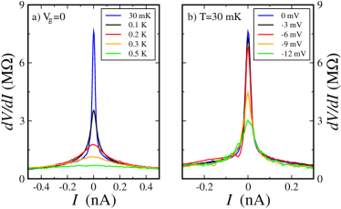
The proximity magnetization can be directly identified in the experimental data. It opens a gap in the one-dimensional spectrum in the vicinity of the contact lunde , which can be seen as a mV width region of high resistance in Fig. 2 (b). This gap only affects the edge channel resistance, and has no effect on its coupling to the ferromagnetic electrode.
The zero-bias resistive region is demonstrated in detail in Fig. 5 as dependencies for the sample B with a metallic gate. It disappears completely above 0.5 K, which is consistent in value with the non-linearity onset mV in Fig. 2 (b). In contrast, the linear branches of the curve are invariant below 1 K, which is also consistent with the reported temperature behavior of the diffusive helical edge state transport at macroscopic distances kvon_temp . The zero-bias resistive region is strongly sensitive to the gate voltage, even if it low enough to have no effect on the bulk carrier concentration, see Fig. 5 (b). The suppression is fully symmetric with respect to a gate voltage sign. We connect it with the edge state structure reconstruction lunde in the vicinity of a ferromagnetic contact (denoted by a blue region in Fig. 4), which, however, needs further investigations. A magnetic field above 0.2 T sharply increases the zero-bias resistive region. This behavior is consistent with a spectrum gap lunde due to proximity magnetization, the gap value can be estimated as meV.
V Conclusion
As a result, we experimentally investigate spin-polarized electron transport between a permalloy ferromagnet and the edge of a two-dimensional electron system with band inversion, realized in a narrow, 8 nm wide HgTe quantum well. In zero magnetic field, we observe strong asymmetry of the edge potential distribution with respect to the ferromagnetic ground lead. This result indicates that the helical edge channel, specific for the structures with band inversion even at the conductive bulk, is strongly coupled to the ferromagnetic side contact, possibly due to the effects of proximity magnetization. It allows selective and spin-sensitive contacting of helical edge states.
Acknowledgements.
We wish to thank V.T. Dolgopolov, V.A. Volkov, I. Gornyi, and T.M. Klapwijk for fruitful discussions. We gratefully acknowledge financial support by the RFBR, RAS and the Ministry of Education and Science of the Russian Federation under Contract No. 14.B25.31.0007.References
- (1) M. König, S. Wiedmann, C. Brüne, A. Roth, H. Buhmann, L. W. Molenkamp, X.-L. Qi, and S.-C. Zhang, Science 318, 766 (2007).
- (2) G. M. Gusev, Z. D. Kvon, O. A. Shegai, N. N. Mikhailov, S. A. Dvoretsky, and J. C. Portal , Phys. Rev. B 84, 121302(R) (2011).
- (3) M. Büttiker, Phys. Rev. B 38, 9375 (1988).
- (4) A. Roth, C. Brüne, H. Buhmann, L. W. Molenkamp, J. Maciejko, X.-L. Qi, and S.-C. Zhang, Science 325, 294 (2009).
- (5) G. M. Gusev, E. B. Olshanetsky, Z. D. Kvon, O. E. Raichev, N. N. Mikhailov, and S. A. Dvoretsky, Phys. Rev. B 88, 195305 (2013)
- (6) B.A. Volkov and O.A. Pankratov, Pis’ma Zh. Eksp. Teor. Fiz. 42, 145 (1985) [JETP Lett. 42, 178 (1985)].
- (7) S. Murakami, N. Nagaosa, S.-C. Zhang, Phys. Rev. Lett. 93, 156804 (2004).
- (8) C. L. Kane, E. J. Mele, Phys. Rev. Lett. 95, 146802 (2005).
- (9) B. A. Bernevig, S.-C. Zhang, Phys. Rev. Lett. 96, 106802 (2006).
- (10) K.C. Nowack, E.M. Spanton, M. Baenninger, M. König, J. R. Kirtley, B. Kalisky, C. Ames, P. Leubner, C. Brüne, H. Buhmann, L. W. Molenkamp, D. Goldhaber-Gordon and K. A. Moler, Nature Materials 12, 787 (2013).
- (11) V.V. Enaldiev, I.V. Zagorodnev, V.A. Volkov, JETP Letters 101, 89 (2015).
- (12) T.L. Schmidt, S. Rachel, F. von Oppen, and L.I. Glazman, Phys. Rev. Lett. 108, 156402 (2012); Nikolaos Kainaris, Igor V. Gornyi, Sam T. Carr, and Alexander D. Mirlin, Phys. Rev. B 90, 075118 (2014).
- (13) Jukka I. Vayrynen, Moshe Goldstein, and Leonid I. Glazman, Phys. Rev. Lett. 110, 216402 (2013); Jukka I. Vayrynen, Moshe Goldstein, Yuval Gefen, and Leonid I. Glazman, Phys. Rev. B 90, 115309 (2014)
- (14) Xiao-Liang Qi, Taylor L. Hughes, and Shou-Cheng Zhang, Nature Physics 4, 273 (2008)
- (15) Anders Mathias Lunde and Gloria Platero, Phys. Rev. B 86, 035112 (2012).
- (16) Z. D. Kvon, E. B. Olshanetsky, D. A. Kozlov, N. N. Mikhailov, and S. A. Dvoretskii, Pis’ma Zh. Eksp. Teor. Fiz. 87, 588 (2008) [JETP Lett. 87, 502 (2008)].
- (17) E. B. Olshanetsky, Z. D. Kvon, N. N. Mikhailov, E. G. Novik, I. O. Parm, and S. A. Dvoretsky, Solid State Commun. 152, 265 (2012).
- (18) Z. D. Kvon, E. B. Olshanetsky, E. G. Novik, D. A. Kozlov, N. N. Mikhailov, I. O. Parm, and S. A. Dvoretsky, Phys. Rev. B 83, 193304 (2011).
- (19) E. B. Olshanetsky, Z. D. Kvon, Y. A. Gerasimenko, V. Prudkoglyad, V. Pudalov, N. N. Mikhailov, and S. A. Dvoretsky, Pis’ma v ZhETF 98, 947 (2013).
- (20) E. B. Olshanetsky, Z. D. Kvon, M. V. Entin, L. I. Magarill, N. N. Mikhailov, I. O. Parm, and S. A. Dvoretsky, JETP Lett. 89, 290 (2009).
- (21) A. Kononov, S.V. Egorov, G. Biasiol, L. Sorba, E.V. Deviatov, Phys. Rev. B 89, 075312 (2014).
- (22) A. Kononov, S. V. Egorov, N. Titova, Z. D. Kvon, N. N. Mikhailov, S. A. Dvoretsky, E. V. Deviatov, JETP Letters, 101, 41 (2015).
- (23) A. Kononov, S. V. Egorov, Z. D. Kvon, N. N. Mikhailov, S. A. Dvoretsky, and E. V. Deviatov Phys. Rev. B 93, 041303(R) (2016).
- (24) D. B. Chklovskii, B. I. Shklovskii, and L. I. Glazman, Phys. Rev. B 46, 4026 (1992).
- (25) E. Ahlswede, J. Weis, K. v. Klitzing, K. Eberl, Physica E, 12, 165 (2002).
- (26) For a review, see, e.g., R. J. Haug, Semicond. Sci. Technol. 8, 131 (1993).
- (27) G. M. Gusev, Z. D. Kvon, E. B. Olshanetsky, A. D. Levin, Y. Krupko, J. C. Portal, N. N. Mikhailov, and S. A. Dvoretsky, Phys. Rev. B 89, 125305 (2014)