Absence of a transport signature of spin-orbit coupling in graphene with indium adatoms
Abstract
Enhancement of the spin-orbit coupling in graphene may lead to various topological phenomena and also find applications in spintronics. Adatom absorption has been proposed as an effective way to achieve the goal. In particular, great hope has been held for indium in strengthening the spin-orbit coupling and realizing the quantum spin Hall effect. To search for evidence of the spin-orbit coupling in graphene absorbed with indium adatoms, we carry out extensive transport measurements, i.e., weak localization magnetoresistance, quantum Hall effect and non-local spin Hall effect. No signature of the spin-orbit coupling is found. Possible explanations are discussed.
pacs:
72.25.Rb 72.80.Vp 73.43.-f 81.05.ueThe intrinsic spin orbit coupling (SOC) in graphene is extremely weakHuertas-Hernando et al. (2006); Min et al. (2006); Yao et al. (2007). Enhancement of the coupling may give rise to a variety of topological phenomena, such as the quantum spin Hall effect (two dimensional topological insulators)Kane and Mele (2005a, b); Weeks et al. (2011); Hu et al. (2012); Jiang et al. (2012); Shevtsov et al. (2012), quantum anomalous Hall effectQiao et al. (2010); Ding et al. (2011); Tse et al. (2011); Qiao et al. (2012); Zhang et al. (2012); Qiao et al. (2013) and Chern half metalsHu et al. (2014). These phenomena are among the hottest topics in condensed matter physics. Moreover, graphene endowed with strong SOC can have potential use in spintronics, as SOC provides a means to control the spin electrically, which is at the heart of spintronics.
Absorption of adatoms has been theoretically proposed as an effective way to enhance SOC in grapheneCastro Neto and Guinea (2009); Ding et al. (2009); Abdelouahed et al. (2010); Qiao et al. (2010); Ding et al. (2011); Tse et al. (2011); Weeks et al. (2011); Dyrdał and Barnaś (2012); Hu et al. (2012); Jiang et al. (2012); Ma et al. (2012); Qiao et al. (2012); Shevtsov et al. (2012); Zhang et al. (2012); Qiao et al. (2013); Gmitra et al. (2013); Ferreira et al. (2014); Hu et al. (2014); Pachoud et al. (2014). By distorting the carbon bondCastro Neto and Guinea (2009); Abdelouahed et al. (2010), breaking the inversion symmetryAbdelouahed et al. (2010); Qiao et al. (2010); Weeks et al. (2011), or mediating the hopping between the second-nearest-neighboursKane and Mele (2005a); Weeks et al. (2011), intrinsic or Rashba SOC can be enhanced or induced. The intrinsic SOC is required for the predicted quantum spin Hall effect, whereas Rashba SOC destroys itKane and Mele (2005a). It has been proposed that if the outer shell electrons of adatoms derive from orbitals, the induced intrinsic SOC always dominates over the induced Rashba interaction. Under this condition, it is possible to realize two dimensional(2D) topological insulators in grapheneWeeks et al. (2011). The most promising candidates are indium and thallium, which can open up a significant topologically nontrivial gap. Further theoretical work has confirmed that the two systems are indeed stable topological insulatorsJiang et al. (2012); Shevtsov et al. (2012).
Two experimental groups have reported angle-resolved photoemission studies on the spin-orbit splitting in a related system, graphene on metal substratesVarykhalov et al. (2008); Dedkov et al. (2008); Rader et al. (2009); Marchenko et al. (2012). Graphene on gold displays a very strong Rashba effect. On the other hand, it has been found that the spin relaxation rate measured by non-local spin valves is not enhanced by gold adatomsPi et al. (2010), suggesting SOC is negligible. Recently, a strong SOC has been observed in hydrogenated graphene and chemical vapor deposited graphene by the spin Hall effect (SHE)Balakrishnan et al. (2013, 2014). Nevertheless, in sharp contrast to numerous theoretical work on this topic, relevant experimental results, especially transport experiments, are scarce. This is in part due to two issues. One is related to the low diffusion barrier for metal adatomsChan et al. (2008), which causes clustering of adatoms at room temperature. The other is oxidation of adatoms.
In this work, we employ an ultra low temperature magnetotransport measurement system, with in situ thermal deposition capability, to circumvent the two aforementioned issues. We choose indium, as it is reckoned by a few theoretical work as an ideal candidateWeeks et al. (2011); Jiang et al. (2012); Shevtsov et al. (2012). Weak localization (WL), quantum Hall effect (QHE) and non-local SHE measurements have been carried out for different indium coverages with the aim of searching for evidence of SOC. Comparison with relevant theories has been made and no signature of SOC has been found. The implications have been discussed.
Graphene flakes were exfoliated from Kish graphite onto 285 nm SiO2/Si substrates. Standard e-beam lithography and metallization processes were used to make Hall bar structures. Electrodes are made of 5 nm Pd/ 80 nm Au. Samples were annealed in Ar/H2 atmosphere at 260 ∘C for 2 hours to remove photoresist and other chemical residues and then transferred into our dilution refrigerator. The system is a modified Oxford dilution refrigerator, in which in situ thermal deposition can be performedParker et al. (2006). Before the first deposition, current annealing was done to clean the surface. During deposition and measurements, the sample temperature was maintained below 5 K. Thus, the thermal diffusion of adatoms was strongly suppressed. Electrical measurements were done by a standard low frequency lock-in technique.
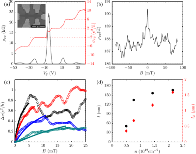
The sample geometry can be seen in the scanning electron microscopy image in Fig. 1(a). The half integer QHE is well developed, which confirms that the sample is monolayer graphene. The low field magnetoresistivity is plotted in Fig. 1(b). The narrow negative magnetoresistivity peak at is WL, while the noise-like but reproducible fluctuations are universal conductance fluctuations. In graphene, electrons are chiral and have a Berry phase , which inverts the constructive interference to a destructive one. Thus, intrinsic graphene should display weak anti-localization (WAL). But, in the presence of intervalley scattering, resulting from short range potential, there will be a crossover from suppressed WL to WAL as the field increasesMcCann et al. (2006); Wu et al. (2007); Tikhonenko et al. (2008). When the intervalley scattering rate exceeds the phase coherence rate, the low field WL correction to the conductivity can be expressed asMcCann and Fal’ko (2012):
| (1) |
where is the digamma function, the elementary charge and the reduced Planck constant. is the diffusion constant and is the phase coherence time. , are the asymmetric and symmetric spin-orbit scattering time, respectively. For pristine graphene, SOC is negligible. To establish the baseline for later comparison, we have measured WL at different gate voltages (carrier densities), shown in Fig. 1(c). Data are fitted to Eq. (1) with only one parameter . To meet the low field requirement of Eq. (1) and also avoid the influence of the universal conductance fluctuations, only the low field positive magnetoconductance are fitted. A good agreement with the theory is found. The mean free path is calculated from the resistivity and carrier density. Considering the charge puddles in graphene, the carrier density at the Dirac point is taken as cm-2Adam et al. (2007). and the phase coherence length are plotted in Fig. 1(d). decreases as one approaches the Dirac point. This is because in graphene is determined by electron-electron interaction, which is enhanced when screening is weakened. The suppression of is further enhanced by the reduction of the mean free time Abrahams et al. (1981).
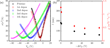
Indium deposition was performed in situ at a very slow rate for several times, each lasting 22 - 300 seconds. During deposition, the sample resistance was monitored so that a desired shift of the Dirac point could be obtained. After each deposition, electrical measurements were carried out. The conductivity as a function of gate voltage is plotted in Fig. 2(a). The Dirac point gradually shifts to negative gate voltage as the indium coverage increases, indicating electron doping. At the same time, the conductivity turns from sublinear to linear in . The linear dependence is attributed to charged impurity scattering being dominantAdam et al. (2007). So, the transition to the linear dependence suggests that indium adatoms mainly introduce charged impurities (long range potential), rather than short range potential. The minimum conductivity at the Dirac point remains relatively constant, about 6, while a closer look shows a slight decrease with increasing adatom density. A similar dependence of has also been observed in potassium absorbed grapheneChen et al. (2008). According to a self-consistent theory proposed by Adams et al.Adam et al. (2007), is a consequence of two competing effects of charged impurities. One is to scatter electrons. The other is to generate a residue carrier density at the Dirac point by doping. The result is a weak negative dependence of on the impurity density. At the same, the width of the plateau increases, which is observed in our experiment. So, all features in the density dependence of the conductivity are consistent with charged impurity scattering. Its implication on SOC will be discussed later.
We now estimate the area density of indium adatoms . Assume that each indium adatom transfers electrons to graphene. If adatoms are dilute, should be a constantAdam et al. (2007). Then, the doped carrier density . can be estimated from the shift of the Dirac point , as . Here is the gate capacitance for 285 nm SiO2 dielectric. The only uncertainty is the value of . According to first-principles calculations, for indium on graphene is Ribeiro et al. (2005); Chan et al. (2008); Weeks et al. (2011). To get an idea of the coverage, we adopt to obtain its lower bound. Consequently, the area density after the third deposition is cm-2, corresponding to a coverage of 0.25%.
From the gate dependence of the conductivity, the field effect mobility is obtained. Its dependence on , which is proportional to , is plotted in Fig. 2(b), as well the mean free path at a carrier density of cm-2. As the mobility is substantially reduced after deposition, it is evident that adatom scattering dominates. We now look for signature of SOC induced by adatoms. WAL has been employed as a sensitive probe for SOCHikami et al. (1980); Bergmann (1982). In conventional 2D electron gases with absence of SOC, the magnetoconductance is positive, the Hallmark of WL, stemming from constructive interference of electrons along time reversal paths. When SOC is turned on, it rotates the electron spin and produces destructive interference, giving rise to WAL, a negative magnetoconductance. W(A)L can be seen as a time-of-flight experiment. Specifically, interactions of a longer time scale manifest themselves in a lower magnetic fieldBergmann (1984). So, as SOC increases, WAL first emerges from zero field and eventually dictates the whole field regime. The conductance correction is given by the HLN equationHikami et al. (1980):
| (2) |
where
Here , . , , represent spin-orbit scattering time and magnetic scattering time, respectively. Since there are no magnetic impurities in our system, we neglect magnetic scattering.
In graphene, the expected evolution of magnetoconductance with increasing SOC is qualitatively similar. The reason is that, although intrinsic graphene display WAL, opposite to conventional 2D electron gases, typical graphene films show WL due to presence of defects. From the theory in Ref. McCann and Fal’ko (2012), the magnetoresistance is given by Eq. (1)McCann and Fal’ko (2012). Compared with conventional 2D electron gases, the effect of SOC on WL depends on symmetry. For asymmetric SOC, normal crossover from WL to WAL occurs, while for symmetric SOC, WL will be suppressed. For adatom absorbed graphene, if any induced SOC, the asymmetric component should be substantialMcCann and Fal’ko (2012). It is anticipated that the magnetoconductance goes from negative to positive as the magnetic field increases. Therefore, both conventional 2D electron gases and graphene are predicted to show similar non-monotonic magnetoconductance. This is the feature that we are particularly interested in.
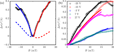
Fig. 3(a) shows the low field magnetoconductance after the third deposition. The magnetoconductance monotonically increases with field, except for universal conductance fluctuations. No trace of WAL near has been found. Fitting of the data to Eq. (1) yields ps, while and are an order of magnitude larger than with significant standard deviations, which essentially suggests inappreciable SOC. We have also performed fitting to Eq. (2). The obtained is similar, ps. Again, is much larger than , consistent with Eq. (1). To illustrate the expected influence of SOC, both equations are plotted with obtained by fitting and all spin-orbit scattering time being equal to . The resultant non-monotonic magnetoconductance is distinct from the experiment data. In fact, extensive measurements of the magnetoconductance at various carrier densities and after each deposition have been carried out and none of them shows WAL around (See supplementary materials). As a comparison, we have also performed the same experiments on deposition of magnesium, which is too light to induce appreciable SOC(See supplementary materials). Qualitatively similar results have been obtained, which confirms absence of induced SOC by In.
Since can be seen as a cut-off time for the quantum interference, it is reasonable to estimate that is longer than at least. For Elliott-Yafet spin-orbit scattering, which is most likely the case for adatoms, . The upper-bound of the spin-orbit coupling strength is then estimated as 12 meV at a carrier density of cm-2. We emphasize that this is the local SOC strength at an adatom, but not the overall spin-orbit gap of 7 meV at a 6% coverage calculated in Ref. Weeks et al. (2011). Because the gap approximately linearly diminishes with the coverage, the upper bound obtained in our experiment is actually much smaller than the prediction.
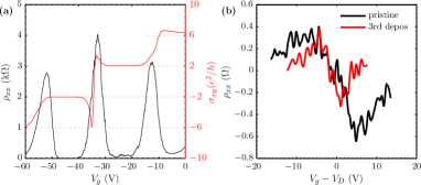
Having not been able to observe SOC through WL, we turn to the quantum Hall effect. The famous half integer Hall effect in graphene stems from the Berry phase of . In the presence of Rashba SOC, the electron spin is locked to its momentumRashba (2009); Zhai and Jin (2014). This spin texture adds another to the Berry phaseZhai and Jin (2014), as in topological insulators. The additional phase is expected to modify the quantum Hall effect. A theory proposes that the spin degeneracy in all Landau levels will be liftedRashba (2009). Since there are two zero modes, one from the level and the other from , the first quantum Hall plateaus stay at (a spacing of ), while the rest are spaced by . We have measured the quantum Hall effect after the second deposition, shown in Fig. 4(a). Despite a reduced mobility, the quantum Hall effect is evident and quantum Hall plateaus remain at their original positions. The predicted lift of the degeneracy for levels is not observed.
Another effect that may arise because of SOC is SHE. In a spin-orbit coupled system, a charge current generates a spin transport in the transverse direction, called SHE, and vice versa, called reverse SHE. The cooperation of two effects leads to a non-local resistanceAbanin et al. (2011),, where is the spin Hall conductivity, is the spin diffusion length, and are the length and width of the sample, respectively. This effect can be used to detect SOC. A large SOC in hydrogenated graphene and chemical vapor deposited graphene has been experimentally confirmed by this methodBalakrishnan et al. (2013, 2014). Here, we have measured the non-local resistance by injecting current through one pair of Hall probes of the Hall bar while monitoring the voltage signal across the other pair of Hall probes. The non-local resistance as a function of the gate voltage before and after deposition is plotted in Fig. 4(b). There is 0.6 Ohm non-local resistance before deposition. This resistance is caused by Ohmic contribution which decays as . After deposition, no substantial change has been observed, indication of no appreciable induced SOC. Taking 0.6 Ohm as the upper-bound of the non-local resistance due to SHE and at a carrier density of cm2/Vs from Ref. Balakrishnan et al. (2013) for hydrogenated graphene, we estimate ps, i.e. 1.3 meV. This is an order of magnitude smaller than the 12 meV upper-bound estimated by WL. It should be pointed out that the estimation here is crude in that is apparently a function of the SOC and unlikely the same as hydrogenated graphene.
Whereas the theories have listed indium as an important candidate for enhancing SOC in graphene and realizing a 2D Topological insulator, we fail to find any signature of SOC by transport measurements. It is noteworthy that the potential of adatoms has been theoretically treated as a short range one, as SOC is induced by mediating the hopping between the first, second and third nearest neighboursPachoud et al. (2014). However, the carrier density dependence of the conductivity doesn’t support considerable increase of short range scattering. Similar observations have been made for magnesium (see supplementary materials) and potassiumChen et al. (2008). The absence of induced SOC may be associated with the lack of short range scattering. The reason for the potential being short range can be accounted for by the Coulomb potential of ionized adatoms, which is long range. We notice that a recent study have shown that titanium particles dope graphene and give rise to long range scattering. But, when these particles are oxidized, accompanied by diminishing doping, significant short range scattering appearsMcCreary et al. (2011). This implies that long range potential could “screen” short range potential. In the presence of a strong long range potential, electrons will have less chance to get close enough to experience the local SOC, which will reduce its average strength. Another possibility is that the bond between indium adatoms and graphene is Van der Waals in nature. The interaction is too weak to modify the hopping between neighbours. Further study may focus on elements that induce less charge transfer, such as Fe or can form a stronger bond to graphene.
Acknowledgements.
This work was supported by National Key Basic Research Program of China (No. 2012CB933404, 2013CBA01603) and NSFC (project No. 11074007, 11222436, 11234001). X. W. thanks P. Xiong for providing details of his in situ deposition design.References
- Huertas-Hernando et al. (2006) D. Huertas-Hernando, F. Guinea, and A. Brataas, Phys. Rev. B 74, 155426 (2006).
- Min et al. (2006) H. Min, J. E. Hill, N. A. Sinitsyn, B. R. Sahu, L. Kleinman, and A. H. MacDonald, Phys. Rev. B 74, 165310 (2006).
- Yao et al. (2007) Y. G. Yao, F. Ye, X. L. Qi, S. C. Zhang, and Z. Fang, Phys. Rev. B 75, 041401 (2007).
- Kane and Mele (2005a) C. L. Kane and E. J. Mele, Phys. Rev. Lett. 95, 226801 (2005a).
- Kane and Mele (2005b) C. L. Kane and E. J. Mele, Phys. Rev. Lett. 95, 146802 (2005b).
- Weeks et al. (2011) C. Weeks, J. Hu, J. Alicea, M. Franz, and R. Wu, Phys. Rev. X 1, 021001 (2011).
- Hu et al. (2012) J. Hu, J. Alicea, R. Wu, and M. Franz, Phys. Rev. Lett. 109, 266801 (2012).
- Jiang et al. (2012) H. Jiang, Z. Qiao, H. Liu, J. Shi, and Q. Niu, Phys. Rev. Lett. 109, 116803 (2012).
- Shevtsov et al. (2012) O. Shevtsov, P. Carmier, C. Groth, X. Waintal, and D. Carpentier, Phys. Rev. B 85, 245441 (2012).
- Qiao et al. (2010) Z. H. Qiao, S. Y. A. Yang, W. X. Feng, W. K. Tse, J. Ding, Y. G. Yao, J. Wang, and Q. Niu, Phys. Rev. B 82, 161414 (2010).
- Ding et al. (2011) J. Ding, Z. Qiao, W. Feng, Y. Yao, and Q. Niu, Phys. Rev. B 84, 195444 (2011).
- Tse et al. (2011) W.-K. Tse, Z. Qiao, Y. Yao, A. H. MacDonald, and Q. Niu, Phys. Rev. B 83, 155447 (2011).
- Qiao et al. (2012) Z. Qiao, H. Jiang, X. Li, Y. Yao, and Q. Niu, Phys. Rev. B 85, 115439 (2012).
- Zhang et al. (2012) H. Zhang, C. Lazo, S. Blügel, S. Heinze, and Y. Mokrousov, Phys. Rev. Lett. 108, 056802 (2012).
- Qiao et al. (2013) Z. Qiao, X. Li, W.-K. Tse, H. Jiang, Y. Yao, and Q. Niu, Phys. Rev. B 87, 125405 (2013).
- Hu et al. (2014) J. Hu, Z. Zhu, and R. Wu, arXiv:1401.5453 (2014).
- Castro Neto and Guinea (2009) A. H. Castro Neto and F. Guinea, Phys. Rev. Lett. 103, 026804 (2009).
- Ding et al. (2009) K.-H. Ding, Z.-G. Zhu, and J. Berakdar, Europhys. Lett. 88, 58001 (2009).
- Abdelouahed et al. (2010) S. Abdelouahed, A. Ernst, J. Henk, I. V. Maznichenko, and I. Mertig, Phys. Rev. B 82, 125424 (2010).
- Dyrdał and Barnaś (2012) A. Dyrdał and J. Barnaś, Phys. Rev. B 86, 161401 (2012).
- Ma et al. (2012) D. Ma, Z. Li, and Z. Yang, Carbon 50, 297 (2012).
- Gmitra et al. (2013) M. Gmitra, D. Kochan, and J. Fabian, Phys. Rev. Lett. 110, 246602 (2013).
- Ferreira et al. (2014) A. Ferreira, T. G. Rappoport, M. A. Cazalilla, and A. H. Castro Neto, Phys. Rev. Lett. 112, 066601 (2014).
- Pachoud et al. (2014) A. Pachoud, A. Ferreira, B. Özyilmaz, and A. H. Castro Neto, Phys. Rev. B 90, 035444 (2014).
- Varykhalov et al. (2008) A. Varykhalov, J. Sánchez-Barriga, A. M. Shikin, C. Biswas, E. Vescovo, A. Rybkin, D. Marchenko, and O. Rader, Phys. Rev. Lett. 101, 157601 (2008).
- Dedkov et al. (2008) Y. S. Dedkov, M. Fonin, U. Rüdiger, and C. Laubschat, Phys. Rev. Lett. 100, 107602 (2008).
- Rader et al. (2009) O. Rader, A. Varykhalov, J. Sánchez-Barriga, D. Marchenko, A. Rybkin, and A. M. Shikin, Phys. Rev. Lett. 102, 057602 (2009).
- Marchenko et al. (2012) D. Marchenko, A. Varykhalov, M. Scholz, G. Bihlmayer, E. Rashba, A. Rybkin, A. Shikin, and O. Rader, Nat Commun 3, 1232 (2012).
- Pi et al. (2010) K. Pi, W. Han, K. M. McCreary, A. G. Swartz, Y. Li, and R. K. Kawakami, Phys. Rev. Lett. 104, 187201 (2010).
- Balakrishnan et al. (2013) J. Balakrishnan, G. Kok Wai Koon, M. Jaiswal, A. H. Castro Neto, and B. Ozyilmaz, Nat. Phys. 9, 284 (2013).
- Balakrishnan et al. (2014) J. Balakrishnan, G. K. W. Koon, A. Avsar, Y. Ho, J. H. Lee, M. Jaiswal, S.-J. Baeck, J.-H. Ahn, A. Ferreira, M. A. Cazalilla, et al., Nat. Commun. 5, 4748 (2014).
- Chan et al. (2008) K. T. Chan, J. B. Neaton, and M. L. Cohen, Phys. Rev. B 77, 235430 (2008).
- Parker et al. (2006) J. S. Parker, D. E. Read, A. Kumar, and P. Xiong, Europhys. Lett. 75, 950 (2006).
- McCann et al. (2006) E. McCann, K. Kechedzhi, V. I. Fal’ko, H. Suzuura, T. Ando, and B. L. Altshuler, Phys. Rev. Lett. 97, 146805 (2006).
- Wu et al. (2007) X. S. Wu, X. B. Li, Z. M. Song, C. Berger, and W. A. de Heer, Phys. Rev. Lett. 98, 136801 (2007).
- Tikhonenko et al. (2008) F. V. Tikhonenko, D. W. Horsell, R. V. Gorbachev, and A. K. Savchenko, Phys. Rev. Lett. 100, 056802 (2008).
- McCann and Fal’ko (2012) E. McCann and V. I. Fal’ko, Phys. Rev. Lett. 108, 166606 (2012).
- Adam et al. (2007) S. Adam, E. H. Hwang, V. M. Galitski, and S. Das Sarma, Proc. Natl. Acad. Sci. USA 104, 18392 (2007).
- Abrahams et al. (1981) E. Abrahams, P. W. Anderson, P. A. Lee, and T. V. Ramakrishnan, Phys. Rev. B 24, 6783 (1981).
- Chen et al. (2008) J. H. Chen, C. Jang, S. Adam, M. S. Fuhrer, E. D. Williams, and M. Ishigami, Nat. Phys. 4, 377 (2008).
- Ribeiro et al. (2005) F. J. Ribeiro, J. B. Neaton, S. G. Louie, and M. L. Cohen, Phys. Rev. B 72, 075302 (2005).
- Hikami et al. (1980) S. Hikami, A. I. Larkin, and Y. Nagaoka, Prog. Theor. Phys. 63, 707 (1980).
- Bergmann (1982) G. Bergmann, Phys. Rev. Lett. 48, 1046 (1982).
- Bergmann (1984) G. Bergmann, Physics Reports 107, 1 (1984).
- Rashba (2009) E. I. Rashba, Phys. Rev. B 79, 161409 (2009).
- Zhai and Jin (2014) X. Zhai and G. Jin, Phys. Rev. B 89, 085430 (2014).
- Abanin et al. (2011) D. A. Abanin, R. V. Gorbachev, K. S. Novoselov, A. K. Geim, and L. S. Levitov, Phys. Rev. Lett. 107, 096601 (2011).
- McCreary et al. (2011) K. M. McCreary, K. Pi, and R. K. Kawakami, Appl. Phys. Lett. 98, 192101 (2011).