Scalable integration of long-lived quantum memories into a photonic circuit
Abstract
We demonstrate a photonic circuit with integrated long-lived quantum memories. Pre-selected quantum nodes - diamond micro-waveguides containing single, stable, and negatively charged nitrogen vacancy centers - are deterministically integrated into low-loss silicon nitride waveguides. Each quantum memory node efficiently couples into the single-mode waveguide ( 1 Mcps collected into the waveguide) and exhibits long spin coherence times of up to 120 s. Our system facilitates the assembly of multiple quantum memories into a photonic integrated circuit with near unity yield, paving the way towards scalable quantum information processing.
pacs:
42.50.Ex, 33.35.+r, 33.50.DqAdvanced quantum information systems, such as quantum computers Bennett and DiVincenzo (2000) and quantum repeaters Briegel et al. (1998), require multiple entangled quantum memories that can be controlled individually Nielsen and Chuang (2000). Over the past decade, there has been rapid theoretical and experimental progress in developing such entangled networks using stationary quantum bits (qubits) connected via photons Cirac et al. (1997); Kimble (2008); Northup and Blatt (2014). Photonic integrated circuits (PICs) could provide a compact, phase-stable, and scalable architecture for such quantum networks. However, the realization of this promise requires the high-yield integration of solid state quantum memories efficiently coupled to low-loss single-mode waveguides.
A promising solid-state quantum memory with second-scale spin coherence times is the negatively charged nitrogen vacancy (NV) center in diamond Maurer et al. (2012); Bar-Gill et al. (2013). Its electronic spin state can be optically initialized, manipulated, measured Doherty et al. (2013), and mapped onto nearby auxiliary nuclear memories Dutt et al. (2007). Quantum network protocols based on these unique qualities have been proposed Childress et al. (2005), and entanglement generation and state teleportation between two spatially separated quantum nodes has been demonstrated Pfaff et al. (2014); Bernien et al. (2013). Translating such entanglement techniques into on-chip architectures promises scalability, but can only succeed if quantum nodes are generated with high yield. So far, yield has been inherently low due to the stochastic process of NV creation, and waveguide patterning in diamond is challenging, preventing low-loss waveguides in the optical domain around 638 nm, the zero phonon line (ZPL) of the NV. Thus, while proof-of-principle network components have been demonstrated Hausmann et al. (2012, 2013), the assembly of a quantum memory device into a PIC has not yet been shown. In contrast to diamond, silicon nitride (SiN)-based photonics relies on well-developed fabrication processes and is CMOS-compatible Moss et al. (2013). Recently, ultra-low-loss channel waveguides ( 0.3 dB/cm) and high-fidelity nonlinear devices have been demonstrated Levy et al. (2010). Moreover, its large band gap (5 eV) and high index of refraction () make it ideal for routing the visible emission of NVs in diamond.
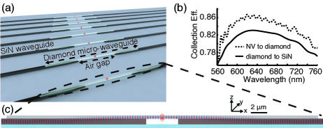
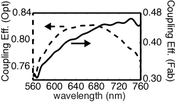
Here, we address the challenges of high yield integration into low-loss photonic networks by integrating pre-selected, long-lived quantum memories based on NV centers into SiN PICs. In our approach, each quantum node consists of a diamond micro-waveguide (WG) suspended over a coupling region in a SiN waveguide, as illustrated in Figure 1(a). The diamond WG supports single mode propagation over the NV emission spectrum with a cross section of 200200 nm. Suspending it across an air gap in the SiN WG enables efficient coupling of the NV to the single optical mode in the diamond WG. Finite Difference Time Domain (FDTD) simulations show that with this air gap, up to 86% (78%) of the NV ZPL (phonon side band) fluorescence intensity at nm (600-780 nm) is guided into the diamond WG with optimal, realistic NV dipole orientation (the projection of the emission dipole along the WG propagation axis is minimized for 100 diamond WG) and optimal NV position (the mode maximum of the diamond WG), as seen in Figure 1b (dashed curve).
The SiN waveguide also supports single mode propagation over the NV emission spectrum with a cross section of 400400 nm. Tapering of the overlapping SiN and diamond regions allows for an approximately adiabatic transition between the diamond and SiN waveguide modes. We performed FDTD simulations to optimize the tapered regions of the diamond and SiN waveguides to maximize the coupling between the diamond and SiN waveguides, as shown in Figure 1. Our simulations indicate that up to 95% of the NV fluorescence emitted into the diamond waveguide is transferred into the SiN waveguide with the optimized overlapping tapering regions shown in Figure 1c (see Appendix). Thus, as shown in Figure 1b (solid curve), we estimate that the total collection efficiency from the NV ZPL through the diamond WG into the SiN WG is 82% for our optimized design (see Figure 1c).
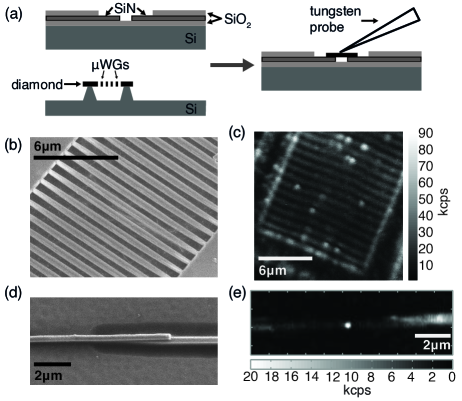
We fabricated the diamond WGs from a 200 nm-thick single crystal diamond membrane which was thinned from a 5 m diamond slab produced by chemical vapor deposition. Natural NVs occurred at a concentration of approximately 0.25 NVs/m3. A patterned silicon membrane is used as a hard etch mask Li et al. (2014) during an oxygen plasma etch of the diamond membrane Li et al. (2013) (see Appendix). We fabricated the SiN waveguides from a 400 nm thick SiN layer deposited on silicon dioxide Levy et al. (2010). The waveguides were cladded with a 3 m layer of SiO2 except for a 50 m window over the coupling region for the integration of the diamond WGs.
Figure 2(b) shows a typical array of diamond WGs. In this experiment, we used 12 m-long, 200 nm wide WGs with 4 m-long tapers down to 100 nm on either side. This minimum taper size is larger than optimal, but fabrication yield was increased as the WGs were connected at these ends. FDTD simulations indicated that this geometry should yield a 52.5% coupling efficiency from the NV ZPL to the SiN waveguide with optimal NV parameters (see Appendix).
After fabrication, we characterized the WGs using a confocal microscope (NA = 0.9) with 532 nm excitation. Using photoluminescence (PL) raster scans, we identified WGs with single NVs near the center as indicated in Figure 2c. A pre-selected diamond WG was picked and transferred onto a SiN coupling region with a tungsten probe, where it adhered due to surface forces (see Appendix). Figure 2d and e show an SEM of the transferred structure and the corresponding PL scan, respectively. This bottom-up integration process ensures that every node contains exactly one NV memory. Such high yield is not possible without pre-selection even when nitrogen atoms are spatially implanted, as the number of NVs generated remains stochastic.
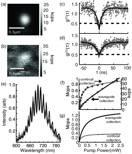
Single NVs in integrated devices were excited from the top with the confocal setup described above and PL was collected via the confocal setup into a single mode fiber (confocal collection) and through the SiN waveguide into a lensed single mode fiber (waveguide collection). In both cases, the collected fluorescence was filtered with a 550 nm long pass filter. We will focus on the optical analysis of the integrated system seen in Figure 2d,e. Figure 3a and b show PL raster scans of the NV under confocal excitation with confocal and waveguide collection, respectively.
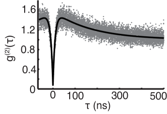
Second order correlation measurements on photons collected via the confocal setup confirm that all NVs in tested WGs show single emitter character, with anti-bunching as low as g (see Appendix), implying that the NVs are extremely well isolated from background sources of fluorescence. Figure 3c shows the normalized auto-correlation measurement of the NV in Figure 3a,b, with g at W of 532 nm excitation. We also performed cross-correlation measurements between photons collected via the confocal and waveguide setups. The normalized histogram in Figure 3d indicates clear anti-bunching at 60W of excitation. We attribute the increase in g from the confocal auto correlation measurement to PL from the SiN waveguide due to coupling of the 532 nm excitation laser into the WG. This PL is also observed in the spectrum collected through the waveguide (see Appendix). This background could be eliminated by fabricating a distributed Bragg reflector at the excitation laser wavelength into the SiN waveguide near the diamond coupling region Harris et al. (2014); Wang et al. (2012). This filter could block scattered laser light from traveling through the SiN WG and exciting background fluorescence.
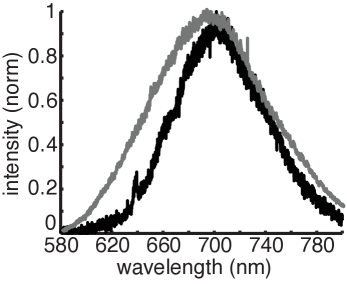
Figure 3e plots the spectrum of the fluorescence collected through the waveguide. An interference pattern is visible, which we attribute to an etalon effect at the diamond end facets. This etalon effect indicates an intensity reflection of and a waveguide group index of 1.7 for the 12 m long diamond WG, which matches our expectations (see Appendix).
To evaluate the enhancement in collection efficiency through the waveguide, we performed emitter saturation measurements with both confocal and waveguide collection as seen in Figure 3f. In each case, the excitation polarization was tuned to maximize the signal-to-noise ratio. For confocal collection, this entailed maximizing the NV excitation rate, while under waveguide collection this entailed limiting the coupling of the 532 nm excitation into the waveguide to minimize background fluorescence. The optimized polarization for waveguide collection reduces the NV excitation rate, and as such increases the saturation intensity from 135 W via confocal collection to 350 W via waveguide collection. For confocal (waveguide) collection, 16 kcps (55 kcps) were detected at 60W of excitation, as used to measure the cross-correlation seen in Figure 3d.
Figure 3g shows the fits in Figure 3f without the linear background terms, and corrected for the measured collection efficiencies of each collection pathway. The waveguide (confocal) collection pathway has a measured efficiency of 25% (17%). Both are measured with an Si avalanche photodiode (APD) with quantum efficiency . Without these system inefficiencies, we estimate that 0.38 NV photons/second are collected into the objective at saturation, while 1.45 NV photons/second are collected into one direction of the single mode SiN waveguide. We integrated 4 such quantum memories into the SiN PIC, each of which contained a single NV center which emitted photons/second into the SiN waveguide at 125 W of excitation (see Appendix).
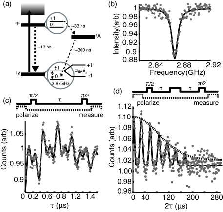
In Figure 4 we present the electron spin properties of the NV center in a second integrated system in which 0.8 photons/second were collected into one direction of the waveguide at saturation. Figure 4a shows the transitions of the NV center with the magnetic sublevels , obtained using optically detected magnetic resonance (ODMR) Manson et al. (2006). Figure 4b plots the ODMR fluorescence signal collected through the waveguide under continuous-wave laser excitation with no external magnetic field.
For state manipulation, the degeneracy of the levels is lifted by the application of an magnetic field of Gauss projected onto the NV axis. A Ramsey sequence, consisting of two pulses separated by a free evolution time , was used to probe the spin environment experienced by the NV. From this, we deduce an ensemble phase coherence time s. We also performed Hahn-echo measurements Hanson et al. (2006), which indicate a spin coherence time of s, see Figure 4d. This long spin coherence time is similar to values observed in the parent diamond crystal Hodges et al. (2012). We anticipate that using isotropically purified 12C diamond, together with dynamical decoupling, should enable spin coherence times in excess of tens of milliseconds Balasubramanian et al. (2009).
In conclusion, we have realized the integration of multiple quantum nodes into a photonic network. Each integrated node contains a single high quality solid-state qubit. The design of the diamond-SiN interface allows for efficient coupling of photons emitted by the NV center into the single mode SiN waveguide, which itself exhibits low propagation loss ( dB/cm) and enables high coupling to single mode fiber ( dB loss). This high collection efficiency into a single spatial mode indicates the promise of this system as an efficient source of single photons in a single spatial mode. Moreover, our experimental results show that each integrated node contained one long-lived quantum memories. Finally, this method can be generalized to other systems (e.g. photonic crystal cavities containing single emitters) to integrate pre-screened functional nodes into high quality PICs with essentially unity yield, paving the way towards scalable on-chip quantum networks.
Acknowledgements.
S.M. was supported by the AFOSR Quantum Memories MURI. T.S. was supported by the Alexander von Humboldt Foundation. E.H.C. was supported by the NASA Office of the Chief Technologist’s Space Technology Research Fellowship. Fabrication and experiments were supported in part by the Air Force Office of Scientific Research (AFOSR Grant No. FA9550-11-1-0014, supervised by Gernot Pomrenke). Research carried out in part at the Center for Functional Nanomaterials, Brookhaven National Laboratory, which is supported by the U.S. Department of Energy, Office of Basic Energy Sciences, under Contract No. DE-AC02-98CH10886. Research also carried out in part at the Cornell NanoScale Facility, a member of the National Nanotechnology Infrastructure Network, which is supported by the National Science Foundation (Grant ECCS-0335765). MLM and DJT was supported by the DARPA Quiness program. We thank Matt Trusheim for valuable discussions.Appendix
Appendix A Simulations
To predict and optimize the coupling efficiency from an NV center to a SiN WG, we simulate our systems using FDTD computations. The NV center is represented as an electric dipole placed in the center of the of a 200 nm x 200 nm diamond WG (), oriented perpendicular to the propagation axis of the WG and 35∘ off-horizontal. This is consistent with a diamond slab oriented in the 100 direction, as we use in our experiment. We placed Poynting flux monitors (i) to either side of the NV, overlapping the diamond WG before the SiN WG begins, (ii) at each end of the SiN WG, and (iii) surrounding the entire structure. These are used to monitor where electro magnetic power is lost; the ratio of (i) to (iii) gives the NV coupling efficiency to the diamond WG, and the ratio of (ii) to (iii) yields the total coupling efficiency of the device.
The optimized device geometry was determined by evaluating the coupling efficiency from the fundamental TE mode of the diamond WG to the SiN WG while sweeping the diamond WG and SiN WG taper lengths. The tapers are aligned such that the taper regions in SiN and diamond do not overlap, minimizing the photon loss. Based on these results, we chose a WG taper length of 6 um and a SiN WG taper length of 5 m. Finally, we use a 2 m gap in the WG to maintain high coupling from the NV into the diamond WG. This results in a WG which is 24 m long, and yields an overall dipole-to-WG coupling efficiency of 83% (41.5% on each side), as seen in Figure 5. We also simulated the structure used in the experiments reported here, which was shorter, and had blunt tips (tapered down to 100 nm instead of 0 nm), increasing losses. This gives a coupling efficiency from the diamond WG to the SiN WG of 52.5%, as seen in Figure 5.
Appendix B Fabrication
We begin fabrication with a 5 m ultra-pure diamond slab produced by chemical vapor deposition. The diamond slab is polished with Ar and Cl2 down to a final thickness of 200 nm. This membrane is patterned with oxygen plasma, using a transferrable patterned silicon membrane as an etch mask, a technique that is introduced and explained in previous publications Li et al. (2014)
Appendix C Diamond Integration
The diamond WGs are detached and picked up from the initial array with a tungsten microprope (Ted Pella) mounted to a 3-axis piezo micromanipulator and rotation stage. The WG is transferred to a SiN chip, which sits on a 2-axis and rotation stage. The diamond WG is aligned to the coupling region of a SiN waveguide and placed in its center. Adhesion is promoted via plasma cleaning of the SiN prior to placement.
Appendix D Photon correlation measurements
Photon correlation measurements were performed with a Hanbury Brown and Twiss setup. In auto-correlation measurements, the PL collected via the confocal setup was coupled to a fiber beam splitter, and the two output arms were coupled to avalanche photon detector (APD) modules (Perkin Elmer). In cross-correlation measurements between confocal and waveguide collection channels, the two single mode collection fibers are directly coupled into separate APDs. A histogram of arrival times was assembled using a time-correlated counting module in start-stop mode. Figure 6 shows an NV in an integrated nanowire exhibiting excellent single photon character with an anti-bunching dip down to 0.07.
Appendix E Waveguide spectra
The PL collected through the waveguide consists of PL originating from the diamond WG and PL caused by laser propagation through the SiN waveguide. The PL originating from the diamond WG experiences an etalon effect due to the diamond WG ends. The detected spectrum is modeled as
| (1) |
where NV is the spectrum collected via the confocal setup (Figure 7a) and BG is the spectrum of the SiN fluorescence collected through the waveguide (Figure 7b). is the expected effective refractive index of the diamond waveguide mode determined via eigenmode analysis of the waveguide, and m is the total length of the diamond waveguide.
Appendix F Scalability
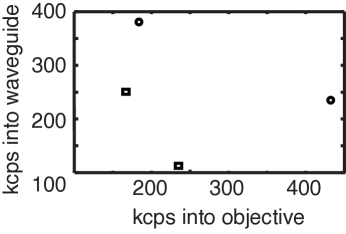
To show the scalability of our method, we integrated 4 WGs into the same SiN PhC and measured NV properties of each through confocal and waveguide collection. Full saturation curves were measured for the points marked with circles. We subtracted the background, and accounted for measured system losses to arrive at the value for counts collected at 125 W excitation. Auto and cross-correlation measurements were taken for the two points marked with squares at 125 W excitation. The depth of the anti-bunching allowed us to subtract background, and measured system losses were accounted for to find the photons per second collected into the objective, or into the SiN waveguide. All showed efficient coupling into the SiN waveguide, with differences perhaps due to NV positioning and orientation.
References
- Bennett and DiVincenzo (2000) Charles H. Bennett and David P. DiVincenzo, “Quantum information and computation,” Nature 404, 247–255 (2000).
- Briegel et al. (1998) H.-J. Briegel, W. Dür, J. I. Cirac, and P. Zoller, “Quantum repeaters: The role of imperfect local operations in quantum communication,” Phys. Rev. Lett. 81, 5932–5935 (1998).
- Nielsen and Chuang (2000) M. A. Nielsen and Isaak Chuang, Quantum computation and quantum information (Cambridge University Press, Cambridge, U.K; New York, 2000).
- Cirac et al. (1997) J. I. Cirac, P. Zoller, H. J. Kimble, and H. Mabuchi, “Quantum State Transfer and Entanglement Distribution among Distant Nodes in a Quantum Network,” Phys. Rev. Lett. 78, 3221–24 (1997).
- Kimble (2008) H.J. Kimble, “The quantum internet,” Nature 453, 1023–30 (2008).
- Northup and Blatt (2014) T.E. Northup and R. Blatt, “Quantum information transfer using photons,” Nature Photon. 8, 356–63 (2014).
- Maurer et al. (2012) P C Maurer, G Kucsko, C Latta, L Jiang, N Y Yao, S D Bennett, F Pastawski, D Hunger, N Chisholm, M Markham, D J Twitchen, J I Cirac, and M D Lukin, “Room-temperature quantum bit memory exceeding one second,” Science 336, 1283–6 (2012).
- Bar-Gill et al. (2013) N. Bar-Gill, L. M. Pham, A. Jarmola, D. Budker, and R. L. Walsworth, “Solid-state electronic spin coherence time approaching one second,” Nat. Commun. 4, 1743 (2013).
- Doherty et al. (2013) M. W. Doherty, N.B. Manson, P. Delaney, Fedor Jelezko, Jörg Wrachtrup, and L C L Hollenberg, “The nitrogen-vacancy colour centre in diamond,” Phys. Rep. (2013).
- Dutt et al. (2007) M V Gurudev Dutt, L Childress, L Jiang, E Togan, J Maze, F Jelezko, A S Zibrov, P R Hemmer, and M D Lukin, “Quantum register based on individual electronic and nuclear spin qubits in diamond,” Science 316, 1312–6 (2007).
- Childress et al. (2005) L Childress, J M Taylor, A. S. Sorensen, and Mikhail D Lukin, “Fault-tolerant quantum repeaters with minimal physical resources and implementations based on single-photon emitters,” Phys. Rev. A 72, 052330 (2005).
- Pfaff et al. (2014) W. Pfaff, B. Hensen, H. Bernien, S.B. van Damm, M.S. Blok, T.H. Taminiau, M.J. Tiggelman, R.N. Schouten, M Markham, D J Twitchen, and R. Hanson, “Unconditional quantum teleportation between distant solid-state quantum bits,” Science 10, 1253512 (2014).
- Bernien et al. (2013) H Bernien, B Hensen, W Pfaff, G Koolstra, M S Blok, L Robledo, T H Taminiau, M Markham, D J Twitchen, L Childress, and R Hanson, “Heralded entanglement between solid-state qubits separated by three metres,” Nature 497, 86–90 (2013).
- Hausmann et al. (2012) Birgit J M Hausmann, Brendan Shields, Qimin Quan, Patrick Maletinsky, M. McCutcheon, Jennifer T. Choy, Thomas M Babinec, A Kubanek, A Yacoby, Mikhail D Lukin, and Marko Loncar, “Integrated diamond networks for quantum nanophotonics,” Nano Lett. 12, 1578–1582 (2012).
- Hausmann et al. (2013) Birgit J.M. Hausmann, Irfan Bulu, P. B. Deotare, M. McCutcheon, V. Venkatraman, M Markham, D J Twitchen, and Marko Loncar, “Integrated high-quality factor optical resonators in diamond,” Nano Lett. , 5791–6 (2013).
- Moss et al. (2013) David J. Moss, Roberto Morandotti, Alexander L. Gaeta, and Michal Lipson, “New cmos-compatible platforms based on silicon nitride and hydex for nonlinear optics,” Nature Photon. 7, 597–607 (2013).
- Levy et al. (2010) Jacob S. Levy, Alexander Gondarenko, Mark A. Foster, Amy C. Turner-Foster, Alexander L. Gaeta, and Michal Lipson, “Cmos-compatible multiple-wavelength oscillator for on-chip optical interconnects,” Nature Photon. 4, 37–40 (2010).
- Li et al. (2014) Luozhou Li, Tim Schroeder, Edward Chen, Michael Walsh, Igal Bayn, Ophir Gaathon, Matthew Trusheim, Ming Lu, Jacob C Mower, Hassaram Bakhru, Matthew Markham, Daniel Twitchen, and Dirk Englund, “Demonstration of a nv spin qubit interacting with a cavity mode in the purcell regime,” CLEO: QELS , FTu3A–4 (2014).
- Li et al. (2013) Luozhou Li, Matthew Trusheim, Ophir Gaathon, Kim Kisslinger, Ching-Jung Cheng, Ming Lu, Dong Su, Xinwen Yao, Hsu-Cheng Huang, Igal Bayn, Abraham Wolcott, Richard M. Osgood Jr., and Dirk Englund, “Reactive ion etching: optimized diamond thin-membrane fabrication for transmission electron microscopy,” JVSTB 35, 06FF01–6 (2013).
- Chen et al. (2013) Edward H. Chen, Ophir Gaathon, Matthew E. Trusheim, and Dirk Englund, “Wide-field multispectral super-resolution imaging using spin-dependent fluorescence in nanodiamonds,” Nano Lett. 13, 2073–2077 (2013).
- SK et al. (2014) Sarkar SK, Bumb A, Wu X, KA Sochacki, P Kellman, MW Brechbiel, and KC Neuman, “Wide-field in vivo background free imaging by selective magnetic modulation of nanodiamond fluorescence,” Biomed. Optics Express 5, 1190–1202 (2014).
- Harris et al. (2014) Nicholas C. Harris, Davide Grassani, Angelica Simbula, Mihir Pant, Matteo Galli, Tom Baehr-Jones, Michael Hochberg, Dirk Englund, Daniele Bajoni, and Christophe Galland, “An integrated source of spectrally filtered correlated photons for large scale quantum photonic systems,” arXiv (2014).
- Wang et al. (2012) Xu Wang, Wei Shi, Han Yun, Samantha Grist, Nicolas A. F. Jaeger, and Lukas Chrostowski, “Narrow-band waveguide bragg gratings on soi wafers with cmos-compatible fabrication process,” Opt. Express 20, 15547–15558 (2012).
- Manson et al. (2006) N.B. Manson, J.P. Harrison, and M.J. Sellars, “Nitrogen-vacancy center in diamond: Model of the electronic structure and associated dynamics,” Phys. Rev. B 74, 104303 (2006).
- Hanson et al. (2006) R Hanson, O. Gywat, and D.D. Awschalom, “Room-temperature manipulation and decoherence of a single spin in diamond,” Phys. Rev. B 74, 161203 (2006).
- Hodges et al. (2012) J. Hodges, L. Li, E. Chen, M. Trusheim, S. Allegri, M. Lu, and D. Englund, “Ultralong spin coherence time 100 nm diamond membranes,” New J. Phys. 14, 093004 (2012).
- Balasubramanian et al. (2009) Gopalakrishnan Balasubramanian, Philipp Neumann, Daniel Twitchen, Matthew Markham, Roman Kolesov, Norikazu Mizuochi, Junichi Isoya, Jocelyn Achard, Johannes Beck, Julia Tissler, Vincent Jacques, Philip R. Hemmer, Fedor Jelezko, and Jorg Wrachtrup, “Ultralong spin coherence time in isotopically engineered diamond,” Nat. Mater. 8, 383–387 (2009).