Interfacial dead layer effects on current-voltage characteristics in asymmetric ferroelectric tunnel junctions
Abstract
Current-voltage characteristics and loops are simulated in SrRuO3/BaTiO3/Pt tunneling junctions with interfacial dead layer. The unswitchable interfacial polarization is coupled with the screen charge and the barrier polarization self-consistently within the Thomas-Fermi model and the Landau-Devonshire theory. The shift of loop from the center position and the unequal values of the positive coercive field and the negative coercive field are found, which are induced by the asymmetricity of interface dipoles. A complete curve of the junction is shown for different barrier thickness, and the effect of the magnitude of interfacial polarization on the tunneling current is also investigated.
pacs:
73.40.Gk, 77.55.fe, 77.80.bnI Introduction
With the development of fabrication technologies, ultrathin ferroelectric films used as tunneling barriers have attracted significant interest in many fieldsScience . Typically, ferroelectric tunnel junction(FTJ) prepared by using an epitaxial ultrathin ferroelectric layer as a tunnel barrier sandwiched between two mental electrodes has brought great progress in experiment and theory nature1 ; nano lett1 . In the past decade, it was shown that ferroelectricity could be maintained in perovskite oxides films with thickness of the order of a few nanometersAPL1 ; PRL1 , these experimental results were consistent with first-principles calculations predicting the critical thickness of ferroelectric barrier could as thin as a few lattice parametersPRL2 , and the existence of ferroelectricity in ultrathin films gives possibilities for nonvolatile memories, such as ferroelectric and muliferroic tunnel junctions. Compared with conventional memories, ferroelectric memories have the advantage of high read and write speed and high density data storagenature1 . The existed researches confirm that the reversal of the electric polarization in ferroelectric barrier produces a change in the electrostatic potential profile across the junction, and this leads to the resistance change which can reach a few orders of magnitude for asymmetric metal electrodesPRL3 . As is well known, interfaces exist inevitably in FTJs, and the interface will give rise to great influence on the transport properties of FTJs. Glinchuk and MorozovskaJPD introduced an interfacial dipole between the ferroelectric thin film and its substrate, and they claimed that the interfacial dipole was originated from the mismatch between the lattice constants and thermal coefficients of the film and its substrate as well as growth imperfections. Duannano lett2 carried out first-principles calculations of KNbO3 thin film placed between two metal electrodes, they found that bonding between the metal and ferroelectric atoms at the interface induced an interfacial dipole moment, which is electrode dependent. LiuPRB1 demonstrated that a BaO/RuO2 interface in SrRuO3/BaTiO3/SrRuO3 epitaxial heterostructure grown on SrTiO3(STO) can lead to a nonswitchable polarization state for thin BaTiO3(BTO) films due to a fixed interfacial dipole, our group also reported that tunneling electroresistance(TER) can be induced by the asymmetric interfaces in a FTJ with symmetric electrodesJAP1 . However, previous studies are focused on the effect of interface on the polarization of ferroelectric barrier, and their efforts are mostly concentrated on zero bias conductance of FTJs, and study of the interfacial effect on the current-voltage characteristics is rare. Natalya A. ZimbovskayaJAP2 and the group of Wenwu CaoJAP3 ; JAP4 had carried out investigations on the current-voltage characteristics of FTJs, but the magnitude and the direction of the barrier’s polarization in their models are given artificially and externally, and the coercive field has not been given within their theoretical studies. In this paper, the typical SrRuO3/BaTiO3/Pt (SRO/BTO/Pt) structure is selected as an example to investigate the transport property of an asymmetric FTJ within the framework of Landau-Devonshire theory and quantum tunneling theory. SrRuO3(SRO) is a suitable oxide electrode for the epitaxial growth due to its similar lattice constant with the substrate and BTO, and Pt is a well conductive metal electrode. The interfacial polarization, inhomogeneous barrier polarization and the screen charge of the electrodes are coupled together in our model, and the coercive field for the switching of barrier polarization is obtained self-consistently. It is found that the interfacial dead layers will have great influence on the hysteresis loop and behavior of FTJs, and shifts of the hysteresis loop and the loop are observed. The effects of the magnitude of interfacial polarization on the tunneling current is also studied, we hope our investigations will bring useful guidance in the studying of the interfacial effects in nanoscale devices.
II Model and Theory
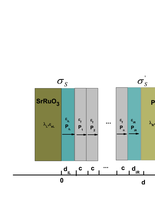
The typical SRO/BTO/Pt junction(See Fig. 1) is used to simulate the and hysteretic behavior of the ferroelectric junction. It is assumed that the polarization of the BTO barrier is orthogonal to the electrode, which can be realized through the misfit compression stress from the substrate. In Fig. 1, PiL and PiR are the polarization of the left and right interface, respectively, and PiL(PiR ) is assumed to be fixednano lett2 . From the first-principles calculations, it is found that the effects of the interfacial dead layer extend for only 1-2 atomic layersPRB2 . Therefore, the thickness of the interface layer is chosen as one unit cell in this paper, i.e., diL=diR=4Å. Based on the lattice model for a strained nanoscale ferroelectric capacitorAPL2 , the average free-energy density of the BTO barrier can be written as
| (1) | |||||
where , , is the dielectric stiffness coefficient at constant strain, , are the elastic compliance, is the electrostricitive coefficient, is the coefficient of the gradient terms in the free-energy expansion, and is the in-plain strain, the tetragonal BTO barrier consists of atomic dipole moments orthogonal to the electrode with an infinite extension along the and axis, the barrier can be divided into layers along axis, where the thickness of each layer is a unit cell. The first summation in Eq. (1) is carried out over all the layers within the barrier. The layer polarization Pi is given by , where , , are the lattice constant along -axis, -axis, and -axis, respectively. The first three terms in the Eq. (1) are the standard Landau-Devonshire energy density, represents the self-electrostatic energy density, is the depolarization field, denotes an additional electrical energy density that is due to an external applied electric field, denotes the gradient energy, which represents the inhomogeneous polarization’s contribution to the free energy density. The last two terms denote the interface contribution to the free-energynano lett2 , is the lattice constant along axis, and () is extrapolation length which represents the discrepancy between the interface and the interior of the thin film.
According to the charge conservation, the magnitude of screening charge density in two electrodes is the same. Under the framework of Thomas-Fermi model, the screening potentials within the left and right electrodes can be written asBOOK1
| (2) |
where () is the screening length in the left (right) electrode, () is the dielectric constant of the left (right) electrode, and is the thickness of the total barrier including the interface layer. Using the continuity conditions of electric displacement vectors and electrostatic potential at the boundaries, we obtain
| (3) |
where and are the dielectric constants of the left and right interface, respectively. , , and are the average spontaneous polarization, the thickness, and the dielectric constant of the BTO barrier. The depolarization fields within the interfaces and each ferroelectric layer have the following form:
| (4) |
The screening lengths for the left and right electrodes are selected as =0.8Å and =0.4Å, and the corresponding dielectric constants are taken as =8.85 and =2, these parameters for the left and the right electrodes are typical values for SRO and Pt electrodesPRL4 , respectively. The magnitude of the interface dielectric constant take the average value and .
The polarization in thermodynamic equilibrium state can be derived by the equations and boundary conditions,
| (5) |
| (6) |
The detail coefficients in Landau free energy in Eq. (5), lattice constants, and the dielectric constants for BTO are listed in Ref. para . As is well known, due to piezoelectric effect, the effective barrier thickness, effect electron mass, and barrier conduction band edge in a FTJ will be changed under an applied electric field. Cao groupJAP4 verified that the depolarization effect is much greater than the piezoelectric effect. Therefore, to avoid extra complications in further computations, the piezoelectric effect is neglected in our following calculations. Within the framework of Landau theory, the microscopic profile of polarization in each ferroelectric layer with consideration of the interfacial dead layer can be calculated numerically, therefore, the electrostatic profile (x) is given as
| (7) |
The overall potential profile across the junction is the superposition of the electrostatic energy potential -e(x), the electronic potential in the electrodes, the rectangular potential () in the left(right) interface, and in FE barrier. Based on the potential energy distribution, the tunneling current through the junction can be calculated, the current per unit area can be derived form the following formulaJAP2
| (8) |
where is the transmission coefficient at the Fermi energy for a given transverse wave vector , the transmission coefficient is obtained by solving numerically the Schrdinger equation for an electron moving in the total potential by imposing a boundary condition of the incident plane wave and by calculating the amplitude of the transmitted plane wave within the formation of transfer matrix, and are Fermi-Dirac distribution functions with chemical potentials , when a nonzero bias voltage V is applied across the junction, and satisfy , and the Fermi-Dirac distribution functions are expressed as and , where is the Boltzmann constant. We also assume the electron has a free electron mass, the Fermi energy is chosen as , and and in the interfaces and the barrierPRL3 .
III Results and Discussions
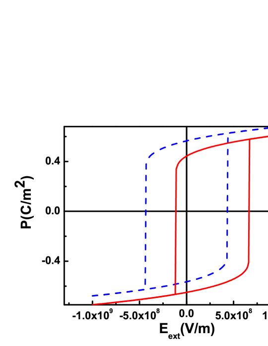
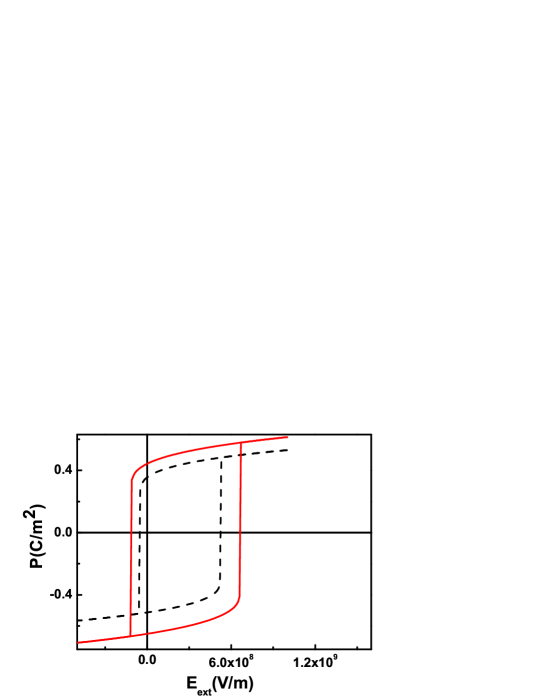
- hysteresis loops of the SRO/BTO/Pt junction are plotted in Fig. 2 and Fig. 3. For simplicity, we use to stand for in this paper, which is the average polarization of the ferroelectric barrier. In SrRuO3/KNbO3/SrRuO3 and Pt/KNbO3/Pt junctions studied in Ref. nano lett2 , the interface dipole moment points to the barrier for SRO electrodes, while the interface dipole moment is pointing to the electrodes for Pt electrodes. Based on first-principles calculations, the BaO/RuO2 interface dipole is nonswitchable and points to the barrier BTOPRB1 . Therefore, the interface polarizations are assumed to be fixed, and take the value of and in studying the hysteresis behavior of SRO/BTO/Pt junctions in this paper, and the positive values of and imply that they are always pointing to the right, as shown in Fig. 1. For a given applied electric field , each can be numerically obtained from Eq. (5). Then, the averaged barrier polarization as a function of is plotted, and the value of coercive field can be found from the P-E loop. The profile of the total potential energy is achieved when each is given, and the tunneling coefficient and consequently the tunneling current can be obtained from Eq. (8). Therefore, the coercive field in the curve in our system is consistent with the ferroelectric switching. From Fig. 2, one can see that a symmetrical loop occurs without consideration of the interfacial layer. The consideration of the interfacial layer will cause a shift of the loop, and the shift takes place along the direction of positive external field. The shift of loop is caused by an intrinsic bias field, which is induced by asymmetric interfacial dipoles, and the direction of the intrinsic bias field is opposite to the external field, therefore, loop will move to the positive direction of the applied field. The offset of loop on the thickness of the barrier is shown in Fig. 3. One can see, from Fig. 3, that the offset increases with the decrease of the barrier thickness under identical interfacial dipoles. As the shift of loop originates from the asymmetric interfacial dipoles, the effect of the interface layer on the hysteresis behavior will become more remarkable for a thinner barrier, so does the offset of loop for the ferroelectric junction with a thinner barrier.
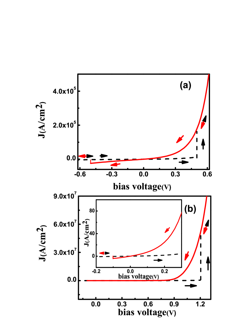
Tunneling currents of SRO/BTO/Pt junctions can be calculated through Eq. (8). The thickness of BTO barrier is selected as 1.6 , and the complete curves are shown in Fig. 4. The dashed lines in Fig. 4 stand for the increasing direction of the scanning voltage, and solid lines correspond to the opposite direction of the scanning voltage. Fig. 4(a) shows the curves for the ferroelectric junction without consideration of interfacial dead layers, and equivalent magnitude of the positive and negative coercive field are obtained at and . With the consideration of interfacial dead layer in Fig. 4(b) (the parameters of the interfacial polarization are the same as those in Fig. 3), the current shows jumps at and , which correspond to the switching of the average spontaneous polarization of BTO. The asymmetry between the positive coercive field and the negative coercive field in curve is also induced by the asymmetric interfacial dipoles, and is similar to the phenomenon mentioned above in the hysteresis behavior.
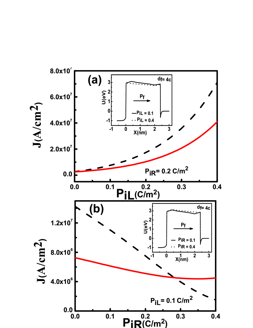
The current density as a function of the magnitude of the interfacial polarization is given in Fig. 5 for a fixed bias voltage 1.0 . Dashed lines correspond to the case for the barrier thickness 1.6 , and solid lines represent the case for 2.4 BTO barrier. Compared Fig. 5(a) with 5(b), it is found that increases with the increase of the magnitude of the left interfacial polarization , while decreases with the increase of . The reason is that the direction of is pointing to the barrier, and the increase of will result in the decrease of the average height of the barrier(See inset in Fig. 5a), while the increase of will give rise an increase of the averaged barrier potential because is pointing away from the barrier(See inset in Fig. 5b). This behavior is analogous to the TER effect in ferroelectric junctions, which has been studied extensively in our previous workJAP6 . One can also see, from Fig. 5, that the current density changes more quickly for the junction with a thinner barrier. This is due to the effect of interface on the transport property becomes more remarkable with the increase of the proportion of interface in ferroelectric junctions with thinner barrier.
In summary, we have investigated the behavior and current-voltage characteristics of the asymmetric ferroelectric tunnel junction with the interfacial dead layer, the inhomogeneous barrier polarization, the interfacial polarization and the screening charge of the electrodes are coupled together in our model, shift of the hysteresis loop and the curve are observed. Effects of the magnitude of the interfacial polarization on the tunneling current are also investigated. As is well known, the structure and property of the interface is very difficult to manipulate and detect. To a certain extent, our model is simply, a more practical thickness, dielectric constant, and polarization of the interface layer are needed to give more reliable simulations. The interface effect of a general FTJ besides the SRO/BTO/Pt junction will be investigated in the future.
Acknowledgements.
This work was supported by the National Science Foundation of China(Grant Nos.11274054, 11047007, 11104193 and 10974140), the QinLan project of Jiangsu Provincial Education Committee, and the open project of Jiangsu Laboratory of Advanced Functional Materials(12KFJJ005).References
- (1) E. Y. Tsymbal and H. Kohlstedt, Science 313, 181 (2006).
- (2) V. Garcia, S. Fusil, K. Bouzehouane, S. Enouz-Vedrenne, N. D. Mathur, A. Barthelemy, and M. Bibes, Nature (London) 460, 81 (2009).
- (3) A. Gruverman, D. Wu, H. Lu, Y. Wang, H. W. Jang, C. M. Folkman, M. Ye. Zhuravlev, D. Felker, C. B. Etom, and E. Y. Tsymbal, Nano Lett. 9, 3539 (2009).
- (4) T. Tybell, C. H. Ahn, and J. M. Triscone, Appl. Phys. Lett. 75, 856 (1999).
- (5) S. K. Streiffer, J. A. Eastman, D. D. Fong, C. Thompson, A. Munkholm, M. V. Ramana Murty, O. Auciello, G. R. Bai, and G. B. Stephenson, Phys. Rev. Lett. 89, 067601 (2002).
- (6) G. Gerra, A. K. Tagantsev, N.Setter, and K. Parlinski, Phys. Rev. Lett. 96, 107603 (2006).
- (7) M. Ye. Zhuravlev, R. F. Sabirianov, S. S. Jaswal, and E. Y. Tsymbal, Phys. Rev. Lett. 94, 246802 (2005).
- (8) M. D. Glinchuk and A. N. Morozovska, J. Phys.: Condens. Matter 16, 3517 (2004).
- (9) C. G. Duan, R. F. Sabirianov, W. N. Mei, S. S. Jaswal, and E. Y. Tsymbal, Nano Lett. 6, 483 (2006).
- (10) X. H. Liu, Y. Wang, P. V. Lukashev, J. D. Burton, and E. Y. Tsymbal, Phys. Rev. B 85, 125407 (2012).
- (11) Y. Z. Wu, J. Appl. Phys. 112, 054104 (2012).
- (12) Natalya A. Zimbovskaya, J. Appl. Phys. 106, 124101 (2009).
- (13) X. Lu, W. Cao, W. Jiang, and H. Li, J. Appl. Phys. 111, 014103 (2012).
- (14) X. Lu, H. Li, and W. Cao, J. Appl. Phys. 112, 054102 (2012).
- (15) W. A. Al-Saidi and A. M. Rappe, Phys. Rev. B 82, 155304 (2010).
- (16) X. Y. Wang, Y. L. Wang, and R. J. Yang, Appl. Phys. Lett. 95, 142910 (2009).
- (17) N. W. Ashcroft and N. D. Mermin, Solid State Physics (Saunders College Publishing, New York, 1976), P. 340.
- (18) D. J. Kim, J. Y. Jo, Y. S. Kim, Y. J. Chang, J. S. Lee, J. G. Yoon, T. K. Song, and T. W. Noh, Phys. Rev. Lett. 95, 237602 (2005).
- (19) For BTO: , , , , , , , , , , , , .
- (20) P. Sun, Y. Z. Wu, T. Y. Cai and S. Ju, Appl. Phys. Lett. 99, 052901 (2011).
Figures’ Caption
FIG.1. Sketch of the asymmetric FTJ with two interfacial
dead layers, and stand for the screening charges in the left and right electrodes, respectively.
FIG.2. hysteresis loops of the SRO/BTO/Pt junction with
interface layers(solid line) and without interface layers (dashed
line). The barrier thickness is 2.4 nm.
FIG.3. loops of the SRO/BTO/Pt junction with
interface layers for different thickness of the BTO barrier: 1.6 nm(dashed line) and 2.4 nm(solid line).
FIG.4. Current-voltage characteristic of SRO/BTO/Pt junction (a)
without consideration of interfacial dead
layers, and (b) with interfacial dead layers. The barrier thickness of BTO is 1.6nm,
arrows indicate scanning directions of the applied voltage, and the
inset in (b) is an enlarged image corresponding to the low range
of the bias voltage.
FIG.5. Current density as a function of (a) the magnitude of the left interface polarization and (b) the magnitude of for
different barrier thickness: 1.6 nm(dashed line) and 2.4 nm(solid line). Here, the bias voltage is taken as 1.0 V. The insets
are the profile of total potential energy for different values of and .