Hybrid quantum circuit with implanted erbium ions
Abstract
We report on hybrid circuit QED experiments with focused ion beam implanted Er3+ ions in Y2SiO5 coupled to an array of superconducting lumped element microwave resonators. The Y2SiO5 crystal is divided into several areas with distinct erbium doping concentrations, each coupled to a separate resonator. The coupling strength is varied from 5 MHz to 18.7 MHz, while the linewidth ranges between 50 MHz and 130 MHz. We confirm the paramagnetic properties of the implanted spin ensemble by evaluating the temperature dependence of the coupling. The efficiency of the implantation process is analyzed and the results are compared to a bulk doped Er:Y2SiO5 sample. We demonstrate the successful integration of these engineered erbium spin ensembles with superconducting circuits.
pacs:
42.50.Pq, 76.30.-v, 61.72.U-, 76.30KgA future quantum information technology will most probably rely on employing different quantum systems, where each subsystem is specialized on fulfilling distinct tasks Wallquist et al. (2009); Xiang et al. (2013). For instance, modern superconducting (SC) quantum circuits are well suited for implementing scalable and fast quantum processors Clarke and Wilhelm (2008). However, these SC qubits suffer from relatively short coherence times Bialczak et al. (2010). In contrast, spin doped solids possess long coherence times of up to a second Tyryshkin et al. (2011) such that they can serve as a quantum memory. Hybrid circuit QED offers a promising way for implementing a complete quantum computer, i.e. a processor interfaced with a memory unit Kubo et al. (2011).
In the recent years, Y2SiO5 (YSO) crystals doped with rare-earth (RE) ions have moved into the focus of quantum information science Lauritzen et al. (2010); Hedges et al. (2010); Clausen et al. (2011). Additionally, strong coherent coupling of Er:YSO to a SC lumped element microwave resonator has been demonstrated Probst et al. (2013). Most of the current research activity relies on RE:YSO crystals which are typically grown using the Czochralski method, where the RE doping takes place during the growth process Usmani et al. (2012); Sabooni et al. (2013); Rieländer et al. (2014).
In this article, we focus on the practical implementation of a hybrid quantum system. In a practical circuit, memory elements need to be placed at specific positions, where they can fulfill their tasks without interfering with the rest of the quantum circuitry. One possible approach is to locally implant spins into an empty crystal or directly into the substrate where the circuit is fabricated on Kolesov et al. (2012). Recently, weak coupling ( 1 MHz) of a superconducting resonator to Gd3+ ions implanted into a sapphire substrate has been reported Wisby et al. (2014). Here, we employ YSO as a host material for RE ions, which promises long optical and spin coherence times Böttger et al. (2006); Bertaina et al. (2007); Rakhmatullin et al. (2009). Moreover, the optical transition of Er3+ lies within the standard telecom C-band, which allows for the implementation of a reversible coherent microwave to optical interface for quantum communication Stannigel et al. (2010); Tian et al. (2004).
In our work, we use a focused ion beam (FIB) to implant Er3+ ions into an undoped Y2SiO5 (YSO) crystal with high spatial resolutionKukharchyk et al. (2014). We then perform circuit QED experiments on these crystals and confirm the successful implantation of erbium ions by studying the electron spin resonance properties at the single photon level.

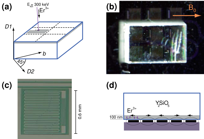
Figure 1(a) shows a sketch of an implantation process. The crystal’s surface is divided into several areas where we implant Er3+ ions in order to study the effect of the amount of implanted ions per area (ion fluence) on the coupling strength and inhomogeneous spin linewidth. Erbium ions were implanted into the YSO crystals in an EIKO-100 FIB system with an energy of 300 keV. The ions were extracted from an Au78.4 Er10 Si11.6 liquid metal ion source (LMIS), developed by A. Melnikov at al.Melnikov et al. (2002). The ion beam was accelerated in a potential of 100 kV and separated into its ion species by a built-in Wien filter. The resolution of the filter does not allow for a fine separation between the Erbium isotopes, but it was possible to minimize the amount of the unwanted 167Er isotope to less than 5%. We estimate the amount of the ion fluence , where is ion current, is the dwell-time of the beam on a single drawing point, and is the area covered by the ion beam.
As the ions penetrate the YSO crystal, they trigger a number of processes in the crystal, mainly ion-ion collisions resulting in lattice defects. The implantation process was simulated with the SRIM software Ziegler et al. (2010), which yields an ion distribution with a mean depth of 60 nm and 39 nm mean deviation Kukharchyk et al. (2014). Since the incident Er3+ beam severely damages the crystal lattice, thermal annealing is employed for its restoration. We have performed both rapid thermal annealing (RTA) and hours long-time annealing.
There are two ways to investigate the properties of implanted ions, either optically, i.e. by confocal photoluminscence Kukharchyk et al. (2014), or in the microwave frequency range using electron spin resonance (ESR). In the case of a magnetic ion, ESR allows to obtain information about the properties of spins in solids, such as g-factors, relaxation and coherence times, and inhomogeneous linewidth Schweiger and Eschke (2001). Typically, 3D resonators deployed in ESR measurements, probe the spins distributed over the whole crystal volume. In contrast, on-chip ESR allows to study the surface region of the paramagnetic sample Schuster et al. (2010); Bushev et al. (2011); Kubo et al. (2012); Sigillito et al. (2014). Since the implanted ions only occupy a region 100 nm below the surface, the on-chip ESR is a convenient tool for this investigation, see Fig. 1(d).
Figure 1(b) shows a picture of the YSO crystal magnetically coupled to an array of superconducting lumped element (LE) resonators Probst et al. (2013). In our work, we investigate two samples (YSO2 and YSO4), which have 5 and 4 implanted areas, respectively. Each implanted area covers one specific LE resonator. An optical micrograph of a single resonator is displayed in Fig. 1(c). The LE resonators covered by the Er:YSO crystal possess loaded quality factors of . The resonance frequencies of the LE resonators cover the frequency range from 4 to 5 GHz.
Figure 1(d) presents a schematic cross-section of the coupling area. The oscillating magnetic field of the microwave penetrates several microns into the crystal, see Ref. Probst et al. (2013) for a simulation of the AC field. A DC magnetic field is applied along the surface of the SC chip. The experiments were carried out inside a BlueFors LD-250 dilution fridge at a base temperature of 25 mK. The on-chip ESR was performed inside a superconducting solenoid coil with a maximum magnetic field of 370 mT.

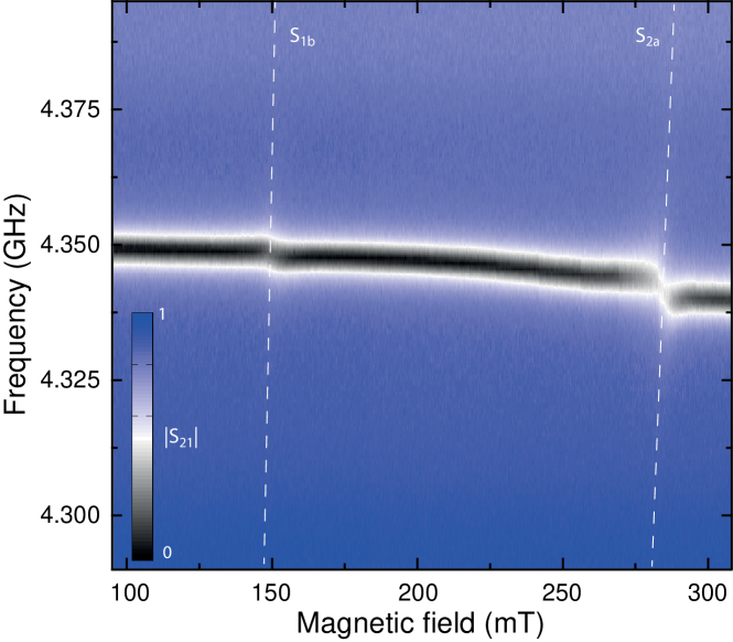
Figure 2 shows the on-chip ESR spectrum of the YSO4 sample area #3. The color plot displays the transmitted amplitude as a function of the magnetic field and the probe frequency. The resonator shows up as a black line which is distorted by two dispersive shifts induced by weakly coupled Er spins Schuster et al. (2010); Bushev et al. (2011). From the spectrum we extract the collective coupling strength and inhomogeneous spin linewidth . In the following, we will focus on the high field transition.
The collective coupling strength of a resonator to a spin ensemble of constant spin density is given by , see Ref. Bushev et al. (2011), where is the frequency of the resonator, the filling factor and the effective g-factor. The collective coupling strength of a spin ensemble of size to the resonator is related to the coupling strength per single spin by . In the limit of weak coupling, where the inhomogeneous linewidth of the spin ensemble exceeds the coupling strength , the HWHM linewidth of the superconducting microwave resonator is given by Bushev et al. (2011)
| (1) |
Here, the spin frequency is given by the Zeeman shift with spin tuning rate . Er spins in YSO possess a large magnetic anisotropy and it was shown that maximum coupling strength is obtained for small DC g-factors and large AC g-factors, respectivelyProbst et al. (2013). The DC g-factors for the high field transition of our samples are 1.09 (YSO4) and (YSO2), respectively, and the orientation of the crystals is shown in Fig. 1(a).

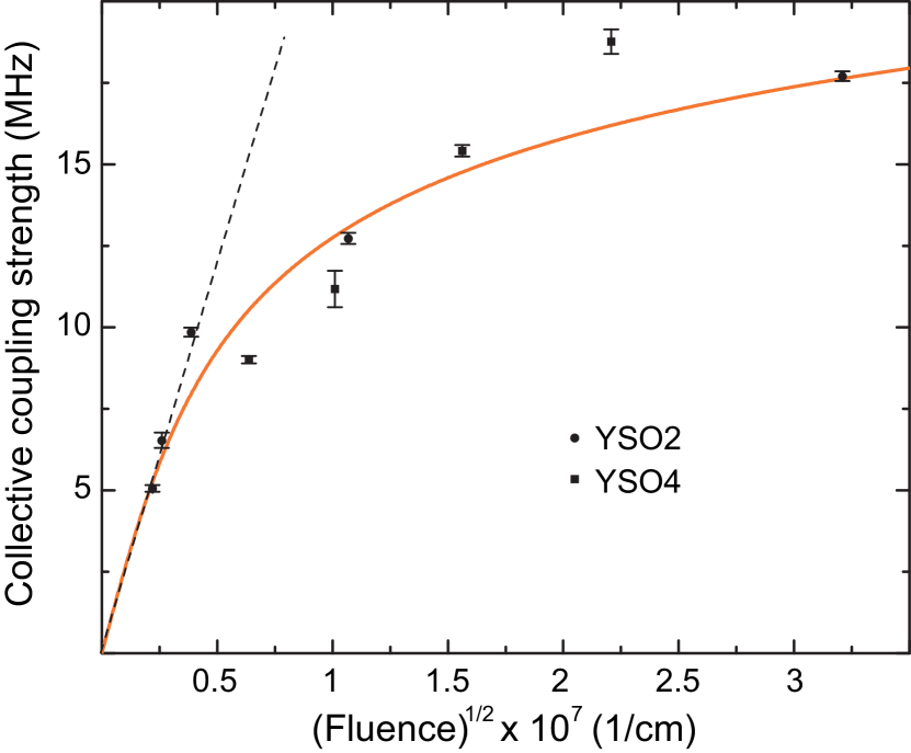
We analyze the spectra of all samples by extracting the collective coupling strength and inhomogeneous spin linewidth as a function of the implanted fluence. The coupling strength varies between 5 MHz and 18.7 MHz, while the linewidths range from 50 MHz to 130 MHz. Figure 3 displays the extracted coupling strengths versus the square root of the fluences. If the implantation process had the same efficiency for all fluences, one would expect the data points to follow a straight line because . However, the coupling strength is not proportional to the square root of the incident fluence and the deviation increases for larger fluences.
In order to interpret this result, it is important to emphasize that the entire sample preparation process consists of FIB irradiation and subsequent annealing in Ar atmosphere. Both processes can provide a contribution to the reduced implantation efficiency. Two samples, which were only treated with RTA, show no ESR response. We found that long term annealing ( 1.5-2 hours) is crucial in order to detect the erbium ions with on-chip ESR. However, a large inhomogeneous spin linewidth remains and does not show a significant dependence on the fluence.
There are two major contributions to the inhomogeneous spin linewidth: Dipole-dipole interaction and local distortions of the crystal field which modulates the effective g-factor. Using Refs. Brown et al. (2011); Bhattacharyya and Chakrabarti (2008), we can estimate an upper limit for the contribution to the inhomogeneous broadening due to dipole-dipole interaction. Assuming the ion distribution calculated by our Monte Carlo simulation, varies from tens of kHz for the lowest fluence to approximately 80 MHz for the sample with the largest fluence.

Since the linewidth always resides at a high level, we conclude that the distorted crystal field dominates the linewidth. The details of the implantation and annealing processes are complex and a more detailed study would be needed to model the entire process.
Since we do not know exactly the distribution of the ions in the crystal and the distortion of the lattice, we use the known implantation process parameter fluence to motivate a simplified empirical model. From all erbium ions per area , which penetrate the sample, only a subset will finally be a in an appropriate configuration. Therefore, merely these ions contribute to the ESR signal and . We assume that the implantation yield (including post-annealing) is exponentially reduced by the amount of ions per implanted area (dose), . Here, is the intensity of the FIB and denotes a critical dose where local interaction effects in the crystal start to dominate over the enhanced amount of erbium ions. The total number of incident ions per area is given by the fluence , where denotes the total implantation time for a given area . The effective implanted dose with respect to the fluence is given by
| (2) |
thus, . The fit to the experimental points is presented in Fig. 3 and yields cm-2. Only in the limit of low fluence , the collective coupling is proportional to the total number of implanted ions.
| crystal ID | YSO2 | YSO4 | bulk | |||||||
|---|---|---|---|---|---|---|---|---|---|---|
| implanted area | #1 | #2 | #3 | #4 | #5 | #1 | #2 | #3 | #4 | Er:YSOProbst et al. (2013) |
| /2 (MHz) | 5.06 | 6.53 | 9.85 | 12.73 | 17.71 | 9.01 | 11.18 | 15.41 | 18.77 | 34 |
| /2 (MHz) | 68.1 | 107 | 105 | 105 | 112 | 48.6 | 136 | 69.2 | 93.1 | 12 |
| (cm-2) | 4.80 | 6.73 | 15.0 | 114 | 1030 | 40.6 | 102 | 244 | 487 | – |
| ‡ (ppm) | 35 | 46 | 81 | 225 | 414 | 145 | 215 | 288 | 348 | 200 |
| () | 14.1 | 18.5 | 32.9 | 90.8 | 167 | 58.4 | 86.8 | 116 | 141 | |
| (Hz) | 85 | 96 | 109 | 85 | 87 | 75 | 76 | 90 | 100 | 76 |
| (s) | † | † | 1.13 | 1.10 | 1.19 | 1.83 | 2.91 | 1.9 | (2)∗ | 4.3 |
| (s) | † | † | 7.36 | 8.16 | 7.49 | 12.2 | 15.6 | 11.9 | (14)♯ | – |
| annealing param. | 2 h at C in Ar atmosphere | 1.5 h at C in Ar atmosphere | – | |||||||
‡assuming an average 60 nm thick layer, ∗uncertainty %, ♯uncertainty %, †SLR signal too weak
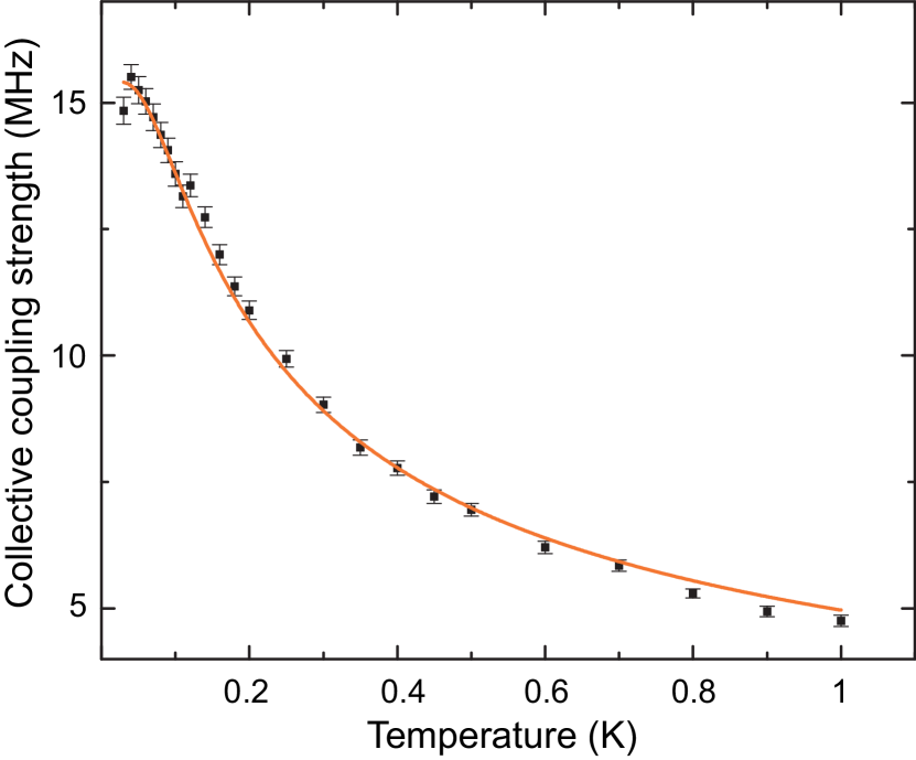
In order to check whether the implanted ions form a paramagnetic spin ensemble, we studied the temperature dependence for sample YSO4 area #3. Figure 4 shows the measured temperature dependence of the collective coupling strength , which nicely follows the theory of paramagnetic crystals
| (3) |
Thus, the implanted ions can be modelled as a system of the independent spins Bushev et al. (2011).
In contrast to the coupling strength the inhomogeneous spin linewidth is about 70 MHz and stays constant in the temperature range from 30 mK up to 1 K. Since crystals grown by the Czochralski method are known to have a much smaller linewidth (12 MHz for 200 ppm doping concentration) at low temperatures Probst et al. (2013), we assume, that the distorted crystal field dominates the inhomogeneous broadening over dynamic effects, in this temperature range.
In the limit of weak coupling where and the cooperativity , we can study the spin relaxation dynamics directly. Here, we employ a technique similar to Ref. Probst et al. (2013). In contrast to that reference, our weakly coupled cavity is equivalent to a long transmission line. The decay rate of the resonator tuned in resonance with the spins is . The amplitude of the depth of the resonator dip is proportional to . The second term in that equation is proportional to the number of participating spins given by the population difference .
An initial strong microwave pulse saturates the spin ensemble and the depth of the resonator dip increases significantly. The resonator is then continuously probed at low power in order to observe the decrease of the resonator dip while the spin ensemble is relaxing back to its equilibrium position. We observe a double exponential decay with two time scales and . This suggests that the energy relaxation is dominated by a direct process on short timescales plus an indirect process on larger timescales. Typically, the spin-lattice relaxation time at low temperatures () is dominated by a direct process , see Ref. Abragam and Bleaney (2012) chapter 10.
Table 1 summarizes the results of our on-chip ESR investigations of implanted Er:YSO samples and compares them to a doped as-grown Er:YSO crystal. We note here, that the implanted crystals have a similar orientation as the bulk doped crystal, see also Ref. Probst et al. (2013). The effective local concentration and number of spins are calculated from and using Eq. (2). All implanted samples couple weakly to the LE resonators because . The linewidth does not show a significant dependence on the coupling strength or fluence. The value of the calculated average single-spin coupling is in accordance with our estimation of Hz using the inductance of the LE resonator Wuensch et al. (2011) and the simulated magnetic field Probst et al. (2013) with an AC g-factor of 15. We detect no significant difference between the YSO2 and the YSO4 samples.
To conclude, erbium ions were successfully implanted by focused ion beam irradiation of a Y2SiO5 substrate. The ions possessed an energy of 300 keV and penetrated up to 100 nm inside the substrate. A subsequent annealing of the samples in argon atmosphere at 1200 ∘C for 1.5-2 hours turned out to be crucial. The implanted spin ensemble was characterized by on-chip ESR spectroscopy at 20 mK and at the single microwave photon limit. The collective coupling strengths of the implanted spins vary from 5 to 18.7 MHz, and exceed the typical dissipation rates of SC circuits. The temperature dependence of the coupling strength shows paramagnetic behavior. The inhomogeneous spin linewidth is 5 to 10 times larger compared to a bulk doped Er:YSO crystal grown by the Czochralski method. In order to reduce the spin linewidth, further investigations of the annealing process are required. We believe that implantation into heated substrates will be crucial for an optimal process. Our work paves the way towards the local integration of erbium spins in SC quantum circuits. This concept can be employed for the reversible conversion of microwave and telecom C-band photons by combining microwave and optical waveguides on the same crystal Schuck et al. (2013); O’Brien et al. (2014).
S. P. acknowledges financial support by the LGF of Baden-Württemberg. We thank Ch. Hintze and M. Drescher for the ESR characterization of undoped and grown YSO crystals. This work was supported in part by the DFG, the BMBF program ”Quantum communications” through the project QUIMP and the Ministry of Education and Science of the Russian Federation under contract no. 11.G34.31.0062. N. K. and A. D. W. acknowledge gratefully support of Mercur Pr-2013-0001, the DFH/UFA CDFA-05-06 and RUB Research School.
References
- Wallquist et al. (2009) M. Wallquist, K. Hammerer, P. Rabl, M. D. Lukin, and P. Zoller, Phys. Scr. T137, 014001 (2009).
- Xiang et al. (2013) Z. Xiang, S. Asshab, J. You, and F. Nori, Rev. Mod. Phys. 85, 623 (2013).
- Clarke and Wilhelm (2008) J. Clarke and F. Wilhelm, Nature 453, 1031 (2008).
- Bialczak et al. (2010) R. C. Bialczak, M. Ansmann, M. Hofheinz, E. Lucero, M. Neeley, A. D. O’Connell, D. Sank, H. Wang, J. Wenner, M. Steffen, A. N. Cleland, and J. M. Martinis, Nat. Phys 6, 409 (2010).
- Tyryshkin et al. (2011) A. M. Tyryshkin, S. Tojo, J. J. L. Morton, H. Riemann, N. V. Abrosimov, P. Becker, H.-J. Pohl, T. Schenkel, M. L. W. Thewalt, K. M. Itoh, and S. A. Lyon, Nat. Mat. 11, 143 (2011).
- Kubo et al. (2011) Y. Kubo, C. Grezes, A. Dewes, T. Umeda, J. Isoya, H. S. N. Morishita, H. Abe, S. Onoda, T. Ohshima, V. Jacques, A. Dréau, J.-F. Roch, I. Diniz, A. Auffeves, D. Vion, D. Esteve, and P. Bertet, Phys. Rev. Lett. 107, 220501 (2011).
- Lauritzen et al. (2010) B. Lauritzen, J. Minář, H. de Riedmatten, M. Afzelius, N. Sangouard, C. Simon, and N. Gisin, Phys. Rev. Lett. 104, 080502 (2010).
- Hedges et al. (2010) M. Hedges, J. Longdell, Y. Li, and M. Sellars, Nature 465, 1053 (2010).
- Clausen et al. (2011) C. Clausen, I. Usmani, F. Bussières, N. Sangouard, M. Afzelius, H. de Riedmatten, and N. Gisin, Nature 469, 508 (2011).
- Probst et al. (2013) S. Probst, H. Rotzinger, S. Wünsch, P. Jung, M. Jerger, M. Siegel, A. V. Ustinov, and P. A. Bushev, Phys. Rev. Lett. 110, 157001 (2013).
- Usmani et al. (2012) I. Usmani, C. Clausen, F. Bussieres, N. Sangouard, M. Afzelius, and N. Gisin, Nat Photon 6, 234 (2012).
- Sabooni et al. (2013) M. Sabooni, Q. Li, S. Kröll, and L. Rippe, Phys. Rev. Lett. 110, 133604 (2013).
- Rieländer et al. (2014) D. Rieländer, K. Kutluer, P. M. Ledingham, M. Gündoğan, J. Fekete, M. Mazzera, and H. de Riedmatten, Phys. Rev. Lett. 112, 040504 (2014).
- Kolesov et al. (2012) R. Kolesov, K. Xia, R. Reuter, R. Stöhr, A. Zappe, J. Meijer, P. Hemmer, and J. Wrachtrup, Nat Commun 3, 1029 (2012).
- Wisby et al. (2014) I. Wisby, S. E. de Graaf, R. Gwilliam, A. Adamyan, S. E. Kubatkin, P. J. Meeson, A. Y. Tzalenchuk, and T. Lindström, Appl. Phys. Lett. 105, 102601 (2014).
- Böttger et al. (2006) T. Böttger, C. W. Thiel, Y. Sun, and R. L. Cone, Phys. Rev. B 73, 075101 (2006).
- Bertaina et al. (2007) S. Bertaina, S. Gambarelli, A. Tkachuk, I. N. Kurkin, B. Malkin, A. Stepanov, and B. Barbara, Nat. Nanotechnol. 2, 39 (2007).
- Rakhmatullin et al. (2009) R. M. Rakhmatullin, I. N. Kurkin, G. V. Mamin, S. B. Orlinskii, M. R. Gafurov, E. I. Baibekov, B. Z. Malkin, S. Gambarelli, S. Bertaina, and B. Barbara, Phys. Rev. B 79, 172408 (2009).
- Stannigel et al. (2010) K. Stannigel, P. Rabl, A. S. Sørensen, P. Zoller, and M. D. Lukin, Phys. Rev. Lett. 105, 220501 (2010).
- Tian et al. (2004) L. Tian, P. Rabl, R. Blatt, and P. Zoller, Phys. Rev. Lett. 92, 247902 (2004).
- Kukharchyk et al. (2014) N. Kukharchyk, S. Pal, J. Rödiger, A. Ludwig, S. Probst, A. V. Ustinov, P. Bushev, and A. D. Wieck, Phys. Status. Solidi (RRL) , DOI 10.1002/pssr.201409304 (2014).
- Melnikov et al. (2002) A. Melnikov, T. Gerya, M. Hillmann, I. Kamphausen, W. Oswald, P. Stauche, R. Wernhardt, and A. Wieck, Nuclear Instruments and Methods in Physics Research Section B: Beam Interactions with Materials and Atoms 195, 422 (2002).
- Ziegler et al. (2010) J. F. Ziegler, M. D. Ziegler, and J. P. Biersack, Nucl. Instrum. and Methods in Phys. Res. B 268, 1818 (2010).
- Schweiger and Eschke (2001) A. Schweiger and G. Eschke, Principles of pulse elecrton paramagnetic resonance (Oxford University Press, Oxford, New York, 2001).
- Schuster et al. (2010) D. I. Schuster, A. P. Sears, E. Ginossar, L. DiCarlo, L. Frunzio, J. J. L. Morton, H. Wu, G. A. D. Briggs, B. B. Buckley, D. D. Awschalom, and R. J. Schoelkopf, Phys. Rev. Lett. 105, 140501 (2010).
- Bushev et al. (2011) P. Bushev, A. K. Feofanov, H. Rotzinger, I. Protopopov, J. H. Cole, C. M. Wilson, G. Fischer, A. Lukashenko, and A. V. Ustinov, Phys. Rev. B 84, 060501(R) (2011).
- Kubo et al. (2012) Y. Kubo, I. Diniz, C. Grezes, T. Umeda, J. Isoya, H. Sumiya, T. Yamamoto, H. Abe, S. Onoda, T. Ohshima, V. Jacques, A. Dréau, J.-F. Roch, A. Auffeves, D. Vion, D. Esteve, and P. Bertet, Phys. Rev. B 86, 064514 (2012).
- Sigillito et al. (2014) A. J. Sigillito, H. Malissa, A. M. Tyryshkin, H. Riemann, N. V. Abrosimov, P. Becker, H.-J. Pohl, M. L. W. Thewalt, K. M. Itoh, J. J. L. Morton, A. A. Houck, D. I. Schuster, and S. A. Lyon, Appl. Phys. Lett. 104, 222407 (2014).
- Brown et al. (2011) R. M. Brown, A. M. Tyryshkin, K. Porfyrakis, E. M. Gauger, B. W. Lovett, A. Ardavan, S. A. Lyon, G. A. D. Briggs, and J. J. L. Morton, Phys. Rev. Lett. 106, 110504 (2011).
- Bhattacharyya and Chakrabarti (2008) P. Bhattacharyya and B. K. Chakrabarti, Eur. J. Phys. 29, 639 (2008).
- Abragam and Bleaney (2012) A. Abragam and B. Bleaney, Electron paramagnetic resonance of transition ions (Oxford University Press, Oxford, 2012).
- Wuensch et al. (2011) S. Wuensch, G. Hammer, T. Kappler, F. Geupert, and M. Siegel, IEEE Transactions on Appl. Superconductivity 21, 752 (2011).
- Schuck et al. (2013) C. Schuck, W. H. P. Pernice, and H. X. Tang, Appl. Phys. Lett. 102, 051101 (2013).
- O’Brien et al. (2014) C. O’Brien, N. Lauk, S. Blum, G. Morigi, and M. Fleischhauer, Phys. Rev. Lett. 113, 063603 (2014).