Edge states of moiré structures in graphite
Abstract
We address the origin of bead-like edge states observed by scanning tunneling microscopy (STM) in moiré patterns of graphite. Low-bias STM measurements indicate these edge states are centered around AB stacking sites, contrarily to the common assumption of them being at AA sites. This shift of the beads intensity with respect to the bulk moiré pattern has been corroborated by a tight-binding calculation of the edge states in bilayer flakes. Our results are valid not only for graphite but also for few-layer graphene, where these states have also been recently observed.
I Introduction
Structural moiré patterns can be found in materials in which two superimposed lattices, with different lattice constant and/or a relative rotation between them are present. With the advent of two-dimensional solids and the possibility of stacking them in diverse ways Geim and Grigorieva (2013), the influence of these moiré superstructures in the electronic structure has to be taken into consideration for a complete description of these materials. Indeed, very recent experiments of graphene over hexagonal boron nitride show an unexpected insulating behavior that might ultimately be related to the moiré superlattice Amet et al. (2013); Yankowitz et al. (2012); Woods et al. (2014).
The physical properties of structures composed of few-layer graphene Novoselov et al. (2004) have been shown to display a dependence on the number of layers. Specifically, when two stacked graphene layers are rotated with respect to each other, a distinctive moiré pattern, linked to the electronic density, develops in the electronic states of the bilayer, being sharper for small rotation angles. In fact, an intriguing dependence with the relative rotation angle (RRA) between layers has been observed in STM measurements. For large RRA (), the system behaves as if the two layers were uncoupled and a linear energy dispersion in momentum is retained, like in monolayer graphene. For RRA below the velocity of the charge carriers is reduced and the STM moiré pattern becomes brighter. Scanning tunneling spectroscopy (STS) measurements have shown an angular dependence of the Van Hove singularities consistent with the development of zero-velocity flat bands. These peculiar features have attracted the attention of the graphene community, and many efforts have been dedicated to study and explain the properties of twisted bilayer graphene and the RRA dependence of its physical properties Lopes dos Santos et al. (2007); Shallcross et al. (2008, 2010); Trambly de Laissardière et al. (2010); Suárez Morell et al. (2010); Mele (2010); Bistritzer and MacDonald (2011); Lopes dos Santos et al. (2012); San-Jose et al. (2012); Trambly de Laissardière et al. (2012); Guohong et al. (2010); Luican et al. (2011); Brihuega et al. (2012); Xian et al. (2011); Suárez Morell et al. (2013); Correa et al. (2014); Suárez Morell et al. (2014).
Besides bilayer graphene, highly oriented pyrolytic graphite (HOPG) is another example of material in which this type of moiré structures has been observed Kuwabara et al. (1990); Rong and Kuiper (1993); Xhie et al. (1993); Rong (1994); Ouseph (1996); Bernhardt et al. (1998); Osing and Shvets (1998); Jasinski et al. (2011); Pong and Durkan (2005). HOPG comprises a large number of micron-size crystallites having random in-plane orientations, and in each crystallite, the graphene layers are stacked in an ABA sequence. The hexagonal unit cell has two non-equivalent sites; the site, where a carbon atom is directly placed above an atom of the underlying layer, and the site, for which the carbon atom lies on a hollow site at the center of an hexagon in the layer below. The difference in the local density of states (LDOS) at both sites explains why STM images of HOPG display a three-fold symmetry instead of six-fold Tománek and Louie (1988). The sites, with larger LDOS, are the bright spots in STM images, while the sites are dark due to a reduced LDOS. Nevertheless, under some experimental conditions, the six bright spots can been observed Wang et al. (2006); Cisternas et al. (2008).
Sometimes, a top layer graphene sheet on HOPG is misoriented with respect to the underlying solid, giving rise to moiré patterns, i.e., forming a superlattice with periodicity in the nanometer range. For several years the origin of these moiré patterns remained a controversial topic, but currently, it is widely accepted that these superstructures in graphitic materials are directly linked to the electronic structure of the rotated layers. In fact, an interesting debate arose with respect to which site in the unit cell was responsible for the bright areas in STM measurements. As bright STM spots measured in Bernal (ABA) HOPG were related to AB sites, some authors also associated the bright areas in moiré patterns to AB stacking. However, density functional theory (DFT) and tight binding (TB) simulations of the electronic structure revealed that the AA site is indeed responsible for the bright regions in STM images Xhie et al. (1993); Rong and Kuiper (1993); Campanera et al. (2007).
Another intriguing aspect of these topographic images are the so-called bead-like features, related to edge states in carbon-based moiré structures. A rotated graphene flake over HOPG presents brighter spots at the edges than in the moiré pattern observed inside the flake. By using STM, Berger et al. Berger et al. (2010) have shown that these edge states do not necessarily follow the symmetry of the bulk moiré pattern if the topographic measurements are performed with a bias voltage of 500 mV. Under these tunneling conditions, a "disordered" decoration on the edges of the top layer is observed. Despite the fact that these bead-like edge states have been detected several times in the last few years Xhie et al. (1993); Sun et al. (2003); Pong et al. (2007); Varchon et al. (2008); Berger et al. (2010); Zhang and Luo (2013), an explanation of their origin is still absent.
In this work we provide a consistent explanation of the bead-like features observed at low bias in STM images. The analysis of STM images of these low-energy features indicates that the bright spots at the edges are not located at AA sites, as it is the case in bulk moiré patterns, but instead they are located at AB edge sites. We explain this result by simulating the LDOS of a rotated flake over graphene and analyzing the energy distribution of their edge states. The LDOS of the edges have maxima at different energies, depending on the edge stacking: AA or AB. The edge states with energies closer to the Fermi level () turn out to be brighter in AB edge sites, in agreement with our STM observations.
II Experimental method
The STM images shown in Fig. 1 were taken from HOPG cleaved in air HOP . The sample was swiftly introduced into an ultra-high vacuum chamber (base pressures below Torr) equipped with a commercial Omicron scanning tunneling microscope. Topographic images were collected at room temperature in a constant current mode, adjusted to 2 nA, and a bias voltage of 100 mV. Nanotec Electronica WSXM software was used for image processing Horcas et al. (2007). Fig. 1(a) shows a region with a distinctive moiré structure, in which bead-like edge states are clearly distinguished. In Figs. 1 (b) and (d) it is possible to observe not only the brighter moiré pattern spots, but also the fainter triangular lattice image displayed by AB stacked graphite in topographic STM measurements. The bright spot in the moiré cell corresponds to the AA region; the rest of the cell is in a large percentage composed of AB-like regions Campanera et al. (2007). As a result one observes the well-known triangular lattice of AB-stacked graphite between the bright spots corresponding to AA sites. The periodicity of the moiré pattern was obtained by superimposing a periodic grid over the image in panel (c). From this graphical procedure, we were able to measure the length of the supercell, which is nm. The periodicity of the supercell is related to the RRA between layers by the equation , where Å is the length of the graphene lattice vector. For this particular pattern this expression yields a value of .
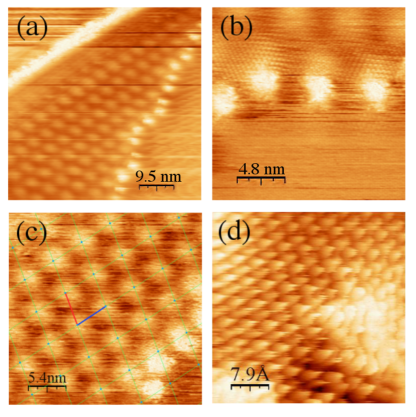
In Figs. 1 (b) and (c), one can observe that the brighter edge states do not follow the periodicity of the bulk moiré pattern. This misalignment of the bright beads at the edges of rotated graphene layers arises from the combination of the moiré enhancement of the local density of states and the presence of edge states due to the termination of the upper graphene layer. With the purpose of explaining these observations, in the following section we describe some theoretical issues related to this system.
III Theoretical considerations
In order to explain the STM images obtained from HOPG it is sufficient to consider only two graphene layers. The relative rotation of one layer with respect to the other is enough to reproduce the moiré pattern observed in infinite systems.
III.1 Geometry
The unit cell of two rotated graphene layers, the so-called twisted bilayer graphene (TBG), is obtained by rotating a Bernal-stacked bilayer. As a reference we choose the rotation axis to be in a B site, which has one atom in the top layer situated on a hollow site, at the center of a hexagon in the layer underneath Suárez Morell et al. (2011), but it can equivalently be taken to be in an A site, where two atoms are exactly on top of each other Campanera et al. (2007). We briefly summarize the notation employed for these structures. A commensurate unit cell (UC) for TBG is built as follows: a point of the crystal with coordinates (n,m integers) is rotated to an equivalent site . Here the graphene lattice vectors are given by and , and Å is the graphene lattice constant. The vectors of the unit cell for TBG can be chosen as and . The corresponding twisted bilayers are usually labeled by the indices Suárez Morell et al. (2010); Trambly de Laissardière et al. (2010). The distance between layers is set to Å.
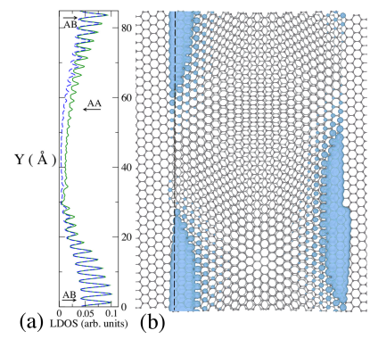
The repetition of a TBG unit cell with along either or , yields a chiral ribbon with edges being predominantly armchair. However, since we focus in edge states, which are produced by zigzag edge atoms Jaskólski et al. (2011), we choose a unit cell along the direction perpendicular to . This particular choice doubles the size of the unit cell, yielding a ribbon with a majority of zigzag edge atoms Suárez Morell et al. (2014). To perform our calculations we extend the size of the lower ribbon to simulate an infinite graphene. The system behaves then like a graphene layer with a flake on top rotated with respect to the lower layer. The right panel of Fig. 2 shows the geometry of the system with a (12,11) moiré pattern. The graphene layer has been cut for illustrative purposes. In the figure is also shown the LDOS of all states integrated from meV to the Fermi energy. The edges are chosen to be minimal, i.e., with a minimum number of atoms, all with coordination number 2. The RRA for this structure in , very close indeed to the actual value experimentally observed.
III.2 Tight-Binding Model
The electronic properties of these bilayer graphene ribbons are modeled within the tight-binding approximation including only orbitals Suárez Morell et al. (2011). Within each layer, we considered a fixed nearest-neighbor intralayer hopping parameter eV. For the interlayer interaction we used a distance-dependent hopping Shallcross et al. (2010); Trambly de Laissardière et al. (2010); Suárez Morell et al. (2010). Thus, the Hamiltonian is given by , where () correspond to the Hamiltonian of each layer and describes the interlayer coupling, , where eV is the nearest-neighbor interlayer hopping energy scale, is the interlayer distance, is the distance between atom on layer and atom on layer , and . This value of accurately reproduces the dispersion bands calculated within a density functional theory approach Suárez Morell et al. (2010); Shallcross et al. (2008). We set a cutoff for the interlayer hopping equal to , with Å being the nearest-neighbor distance between carbon atoms.
IV Discussion
Figs. 2 (a) and (b) show that the LDOS of states with energies very close to the Fermi level are mainly located at AB-stacked edge regions, whereas the AA-stacked sections of the edges do not show any appreciable density of states. Fig. 2 (a) presents a line profile of the LDOS along the left edge of the flake. Arrows indicate the position of AA and AB sites at the edge. Clearly, the LDOS is higher at the AB sites. Calculations were made integrating the LDOS from 100 meV below the Fermi level to (dashed line) and for states with energies between meV and (solid line). The LDOS is higher at the AB sites in both cases, but for the wider integration range an increase in the LDOS at the AA sites is observed. This simulation implies that when a topographic STM image of such system is taken with tip voltages around 100 mV, bright regions at the edges should correspond to AB sites, while non-edge areas are brighter in AA regions. For large tip voltages, around 500 mV, the bright areas at the edges will be also the AB sites, but under some experimental conditions the AA sites might also be visible, creating an smearing pattern in some regions Berger et al. (2010).
This effect can also be explained in a qualitative manner using the band structure of bilayer graphene nanoribbons with AA and AB stacking Suárez Morell et al. (2014), together with the different coupling strengths in AA and AB-stacked edges.
In Figs. 3 (a) and 3 (b) we show the bands of zigzag ribbons with AB and AA stacking respectively, calculated with the same model used for the twisted bilayer nanoribbon (TBNR). By simply counting the edges in each system, four edge bands are expected for both cases Jaskólski et al. (2011). Indeed, for AB stacking there are four edge bands clearly identified in Fig. 3 (a), which are degenerate at the first Brillouin zone boundary at zero energy. The bands for the AA-stacked ribbons show two Dirac points shifted from the BZ boundary; in this case, the edge bands are flat and split by , if only vertical hoppings are considered. Within the model employed in this work, which takes into account interlayer hoppings within a circle of radius , the splitting gives then an idea of the effective interlayer coupling, that it is related to the bonding-antibonding nature of the AA states.
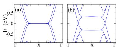
Thus, in AB-stacked edges a large LDOS at (0 eV) can be expected, while for edges with AA stacking, the peaks in the LDOS due to the edges are expected to be shifted below by an energy roughly given by the interlayer coupling.
These energy differences explains why in the STM scans at low bias the bright spots at the edges, the so-called beads, are shifted with respect to the bright areas of the bulk moiré pattern (AA-stacked regions). The bulk regions of the moiré pattern are bright in STM images due to the larger LDOS near . However, close to the edges, the maximum in the LDOS shifts to the AB sites. The low-bias topographic images shown in Fig. 1 are consistent with this result, as well as with the calculated LDOS of the ribbon shown in Fig. 2. Since the STM images were collected with a bias voltage of 100 meV, the bright beads appear only in the AB edges, which are the sites of the only accessible states at that tip bias.
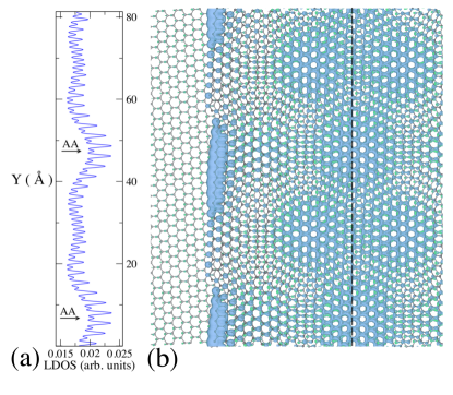
Our model also describes adequately the coexistence of edge and bulk moiré states. To display this feature we have calculated the electronic structure of a very wide graphene flake on top of graphite, in order to obtain also the bulk states. Fig. 4 shows the LDOS for such a system integrated in an energy range between meV and . The line profile in Fig. 4 (a) of the STM simulation is taken along the center of the flake. It shows that states at the AA sites of the bulk are the brightest. Here the arrows indicate the position of AA sites of the bulk. In Fig. 4 (b) the coexistence of both types of states can be observed. The edge states are observed to be misaligned with respect to the moiré pattern displayed by the rotated layer, as it also happens to the experimental results shown in Fig. 1.
V Conclusions
In this work we have addressed a phenomenon observed for several years, but not properly explained to date. By using a TB model to describe the chiral edge states in moiré nanoribbons, we show that bead-like edge states correspond to AB regions of the moiré edges in graphite superstructures. The electrons with low energies in the bulk are localized in AA regions, while at the edges they remain confined at AB-stacked regions. This explanation considers the usual polarization voltages used in STM measurements, i.e., low values around 100 mV. For higher bias voltages the calculation predicts less pronounced differences between AA and AB regions in STM images. Consistently, a mixture of both types of states has also been observed experimentally.
Acknowledgements.
This work has been partially supported by Spanish Ministry of Economy and Competitiveness under grant FIS2012-33521, and Chilean FONDECYT grants 1130950 and 1110935.References
- Geim and Grigorieva (2013) A. K. Geim and I. V. Grigorieva, Nature 499, 419 (2013).
- Amet et al. (2013) F. Amet, J. R. Williams, K. Watanabe, T. Taniguchi, and D. Goldhaber-Gordon, Phys. Rev. Lett. 110, 216601 (2013).
- Yankowitz et al. (2012) M. Yankowitz, J. Xue, D. Cormode, J. D. Sanchez-Yamagishi, K. Watanabe, T. Taniguchi, P. Jarillo-Herrero, P. Jacquod, and B. J. LeRoy, Nature Physics 8, 382 (2012).
- Woods et al. (2014) C. R. Woods, L. Britnell, A. Eckmann, R. S. Ma, J. C. Lu, H. M. Guo, X. Lin, G. L. Yu, Y. Cao, R. V. Gorbachev, A. V. Kretinin, J. Park, L. A. Ponomarenko, M. I. Katsnelson, Y. N. Gornostyrev, K. Watanabe, T. Taniguchi, C. Casiraghi, H.-J. Gao, A. K. Geim, and K. Novoselov, Nature Physics 10, 451 (2014).
- Novoselov et al. (2004) K. S. Novoselov, A. K. Geim, S. V. Morozov, D. Jiang, Y. Zhang, S. V. Dubonos, I. V. Gregorieva, and A. A. Firsov, Science 306, 666 (2004).
- Lopes dos Santos et al. (2007) J. M. B. Lopes dos Santos, N. M. R. Peres, and A. H. Castro Neto, Phys. Rev. Lett. 99, 256802 (2007).
- Shallcross et al. (2008) S. Shallcross, S. Sharma, and O. A. Pankratov, Phys. Rev. Lett. 101, 056803 (2008).
- Shallcross et al. (2010) S. Shallcross, S. Sharma, E. Kandelaki, and O. A. Pankratov, Phys. Rev. B 81, 165105 (2010).
- Trambly de Laissardière et al. (2010) G. Trambly de Laissardière, D. Mayou, and L. Magaud, Nano Letters 10, 804 (2010).
- Suárez Morell et al. (2010) E. Suárez Morell, J. D. Correa, P. Vargas, M. Pacheco, and Z. Barticevic, Phys. Rev. B 82, 121407 (2010).
- Mele (2010) E. J. Mele, Phys. Rev. B 81, 161405 (2010).
- Bistritzer and MacDonald (2011) R. Bistritzer and A. H. MacDonald, PNAS 108, 12233 (2011).
- Lopes dos Santos et al. (2012) J. M. B. Lopes dos Santos, N. M. R. Peres, and A. H. Castro Neto, Phys. Rev. B 86, 155449 (2012).
- San-Jose et al. (2012) P. San-Jose, J. González, and F. Guinea, Phys. Rev. Lett. 108, 216802 (2012).
- Trambly de Laissardière et al. (2012) G. Trambly de Laissardière, D. Mayou, and L. Magaud, Phys. Rev. B 86, 125413 (2012).
- Guohong et al. (2010) L. Guohong, A. Luican, J. M. B. Lopes dos Santos, A. H. Castro Neto, A. Reina, J. Kong, and E. Y. Andrei, Nature Physics 6, 109 (2010).
- Luican et al. (2011) A. Luican, G. Li, A. Reina, J. Kong, R. R. Nair, K. S. Novoselov, A. K. Geim, and E. Y. Andrei, Phys. Rev. Lett. 106, 126802 (2011).
- Brihuega et al. (2012) I. Brihuega, P. Mallet, H. González-Herrero, G. Trambly de Laissardière, M. M. Ugeda, L. Magaud, J. M. Gómez-Rodríguez, F. Ynduráin, and J.-Y. Veuillen, Phys. Rev. Lett. 109, 196802 (2012).
- Xian et al. (2011) L. Xian, S. Barraza-Lopez, and M. Y. Chou, Phys. Rev. B 84, 075425 (2011).
- Suárez Morell et al. (2013) E. Suárez Morell, M. Pacheco, L. Chico, and L. Brey, Phys. Rev. B 87, 125414 (2013).
- Correa et al. (2014) J. D. Correa, M. Pacheco, and E. Suárez Morell, Journal of Materials Science 49, 642 (2014).
- Suárez Morell et al. (2014) E. Suárez Morell, R. Vergara, M. Pacheco, L. Brey, and L. Chico, Phys. Rev. B 89, 205405 (2014).
- Kuwabara et al. (1990) M. Kuwabara, D. R. Clarke, and D. A. Smith, Applied Physics Letters 56 (1990).
- Rong and Kuiper (1993) Z. Y. Rong and P. Kuiper, Phys. Rev. B 48, 17427 (1993).
- Xhie et al. (1993) J. Xhie, K. Sattler, M. Ge, and N. Venkateswaran, Phys. Rev. B 47, 15835 (1993).
- Rong (1994) Z. Y. Rong, Phys. Rev. B 50, 1839 (1994).
- Ouseph (1996) P. J. Ouseph, Phys. Rev. B 53, 9610 (1996).
- Bernhardt et al. (1998) T. Bernhardt, B. Kaiser, and K. Rademann, Surface Science 408, 86 (1998).
- Osing and Shvets (1998) J. Osing and I. Shvets, Surface Science 417, 145 (1998).
- Jasinski et al. (2011) J. B. Jasinski, S. Dumpala, G. U. Sumanasekera, M. K. Sunkara, and P. J. Ouseph, Applied Physics Letters 99, 073104 (2011).
- Pong and Durkan (2005) W.-T. Pong and C. Durkan, Journal of Physics D: Applied Physics 38, R329 (2005).
- Tománek and Louie (1988) D. Tománek and S. G. Louie, Phys. Rev. B 37, 8327 (1988).
- Wang et al. (2006) Y. Wang, Y. Ye, and K. Wu, Surface Science 600, 729 (2006).
- Cisternas et al. (2008) E. Cisternas, M. Flores, and P. Vargas, Phys. Rev. B 78, 125406 (2008).
- Campanera et al. (2007) J. M. Campanera, G. Savini, I. Suarez-Martinez, and M. I. Heggie, Phys. Rev. B 75, 235449 (2007).
- Berger et al. (2010) C. Berger, J.-Y. Veuillen, L. Magaud, P. Mallet, V. Olevano, M. Orlita, P. Plochocka, C. Faugeras, G. Martinez, M. Potemski, C. Naud, L. P. Lévy, and D. Mayou, Int. J. Nanotechnol. 7, 383 (2010).
- Sun et al. (2003) H.-L. Sun, Q.-T. Shen, J.-F. Jia, Q.-Z. Zhang, and Q.-K. Xue, Surface Science 542, 94 (2003).
- Pong et al. (2007) W.-T. Pong, J. Bendall, and C. Durkan, Surf. Sci. 601, 498 (2007).
- Varchon et al. (2008) F. Varchon, P. Mallet, L. Magaud, and J.-Y. Veuillen, Phys. Rev. B 77, 165415 (2008).
- Zhang and Luo (2013) X. Zhang and H. Luo, Applied Physics Letters 103, 231602 (2013).
- (41) ZYA grade HOPG from SPI Supplies / Structure Probe, Inc., 206 Garfield Ave, West Chester, PA 19380-4512, USA.
- Horcas et al. (2007) I. Horcas, R. Fernández, J. M. Gómez-Rodríguez, J. Colchero, J. Gómez-Herrero, and A. M. Baro, Review of Scientific Instruments 78, 013705 (2007).
- Suárez Morell et al. (2011) E. Suárez Morell, P. Vargas, L. Chico, and L. Brey, Phys. Rev. B 84, 195421 (2011).
- Jaskólski et al. (2011) W. Jaskólski, A. Ayuela, M. Pelc, H. Santos, and L. Chico, Phys. Rev. B 83, 235424 (2011).