Characterization of Interface Traps in SiO2/SiC Structures Close to the Conduction Band by Deep-Level Transient Spectroscopy
Abstract
The effects of the oxidation atmosphere and crystal faces on the interface-trap density was examined by using constant-capacitance deep-level transient spectroscopy to clarify the origin of them. By comparing the DLTS spectra of the low-mobility interfaces oxidized in a N2O atmosphere with those of the high-mobility interfaces on C-face oxidized in a wet atmosphere, it was found that a high density of traps are commonly observed around the energy of 0.16 eV from the edge of the conduction band ( traps) in low-mobility interfaces irrespective of crystal faces. It was also found that the generation and elimination of traps specific to crystal faces: (1) the traps can be eliminated by wet oxidation only on the C-face, and (2) the traps (0.37 eV) can be observed in the SiC/SiO2 interface only on the Si-face. The generation of traps on the Si-face and the elimination of traps on the C-face by wet oxidation may be caused by the oxidation reaction specific to the crystal faces.
I Introduction
SiC metal–oxide–semiconductor field-effect transistors (MOSFETs) are regarded as promising candidates for the next-generation high-voltage electrical power switches owing to the high critical electric field of SiC Palmour et al. (1993); Cooper (1997); Baliga (2005). However, the low mobility in the SiC/SiO2 interfaces hinders the potential performance of SiC MOSFETs. Thus, the improvement in the mobility in the SiC/SiO2 interfaces is a central issue in the research and development of SiC MOSFETs. It was presumed that the traps in the SiC/SiO2 interfaces are closely related to the degradation in mobility Afanas’ev et al. (1997). In 2000, Saks and Agarwal clearly showed that the low mobility in the SiC/SiO2 interfaces is caused by the trapping of electrons at the high-density interface traps on the bases of the Hall effect measurements of SiC MOSFETsSaks and Agarwal (2000). They showed that most of the inversion electrons induced by the gate voltage were trapped by interface traps by comparing the free carrier density in an interface obtained by Hall measurements with the total number of inversion electrons. They also pointed out that the Coulombic scattering by the trapped electrons may dominate the inversion electron transport by examining the temperature dependence of the Hall mobility. Later, detailed studies on the inversion electron transport of various types of SiC MOSFETs using Hall measurements confirmed the above-described degradation mechanism in mobility Tilak (2009); Dhar et al. (2010).
Therefore, great efforts have been focused on reducing the interface trap density to improve mobility by examining the gate-oxidation and post-gate-oxidation annealing processes in detail. In recent years, annealing or oxidation in a nitric oxide (NO) or nitrous oxide (N2O) atmosphere, which is hereinafter collectively referred to as oxynitridation, has been used to reduce the high density of interface traps Jamet et al. (2001); Chung et al. (2001); Rozen et al. (2009). The optimized oxynitridation process reduces the interface trap density () evaluated by using the conventional Hi-Lo method Nicollian and Brews (2002) down to less than 1012 cm-2/eV at = 0.2 eV, where and are referred to as the conduction-band edge and energy, respectively Suzuki et al. (2009a). However, the effect of oxynitridation on the mobility is limited. In fact, the mobility in the SiC/SiO2 interfaces fabricated by using oxynitridation is typically approximately 30 cm2/(Vs) Suzuki et al. (2009a); Rozen et al. (2010). Another way to improve the channel mobility is to combine the use of the C-terminated face (C-face) instead of the Si-terminated face (Si-face) along with annealing or oxidation in a wet atmosphere. The typical mobility in the SiC/SiO2 interfaces fabricated on the C-face by using wet oxidation is approximately 90 cm2/(Vs) Fukuda et al. (2004); Suzuki et al. (2009b). However, the cause of the relatively low mobility of the oxynitrided interface could not yet be identified. The densities of interface traps characterized by using the conventional Hi-Lo method are not correlated with the mobilities between these two types of samples Suzuki et al. (2009a, b); thus, it seems that would not be the cause of the relatively low mobility of the oxynitrided interface.
The authors reported that the close to the conduction band in SiC/SiO2 interfaces fabricated using oxynitridation was much higher than that of SiC/SiO2 interfaces fabricated using wet oxidation on C-face by using constant-capacitance deep-level transient spectroscopy (CCDLTS) characterization. T.Hatakeyama et al. (2013). They concluded that the low mobility in SiC/SiO2 interfaces oxidized in a N2O atmosphere on C-face should be caused by trapping electrons in the high density of the traps close to the conduction band. In this study, the effects crystal faces and oxidation atmosphere on the traps in SiC/SiO2 interfaces was examined to confirm that the high density of the traps close to the conduction band are the common cause of the low mobility in SiC/SiO2 interfaces irrespective of the crystal faces. Further, to elucidate the origin of the traps in SiC/SiO2 interfaces, the properties of the identified traps close to the conduction band are discussed according to the dependence of the CCDLTS spectra on the crystal face and oxidation condition.
II Experimental Methods
The samples characterized in this study were MOS capacitors on the C-face or Si-face of 4H-SiC n-type epitaxial wafers. The density of nitrogen in the epitaxial layer was approximately cm-3. The SiC/SiO2 interfaces of the MOS capacitors were fabricated by using the following gate-oxidation processes: (1) oxidation in an O2 atmosphere at 1250 , followed by wet oxidation at 900 , followed by H2 anneal at 800 on the C-face (DWHC); (2) oxidation in a N2O atmosphere at 1250 , followed by a H2 anneal at 1000 on the C-face (NHC); (3) oxidation in an O2 atmosphere at 1250 , followed by wet oxidation at 900 on the Si-face (DWS); and (4) oxidation in an O2 atmosphere at 1250 , followed by post-oxidation annealing in a N2O atmosphere at 1250 , followed by H2 anneal at 800 on the Si-face (DNHS). The thickness of the oxide layer is approximately 50 nm, and the gate electrode is aluminum. The mobilities of the MOSFETs fabricated by using the processes of DWHC, NHC, DWS, and DNHS are approximately 80 cm2/(Vs), 30 cm2/(Vs), 8 cm2/(Vs), and 30 cm2/(Vs), respectively Suzuki et al. (2009b, a); Hatakeyama et al. (2005).
CCDLTS spectra were obtained by measuring the transient voltage signal generated by a feedback loop to maintain the capacitance at a constant value during the measurement of MOS capacitors in the temperature range from 80 K to 400 K. The pulse and reverse bias voltage were approximately 6 V and V, respectively. The capacitance at the reverse bias was kept constant during the temperature scan. For the analysis of the transient voltage signal at each temperature, a deep-level transient Fourier spectroscopy (DLTFS) technique was used Weiss and Kassing (1988); Weiss (1991).

III Results and Discussion
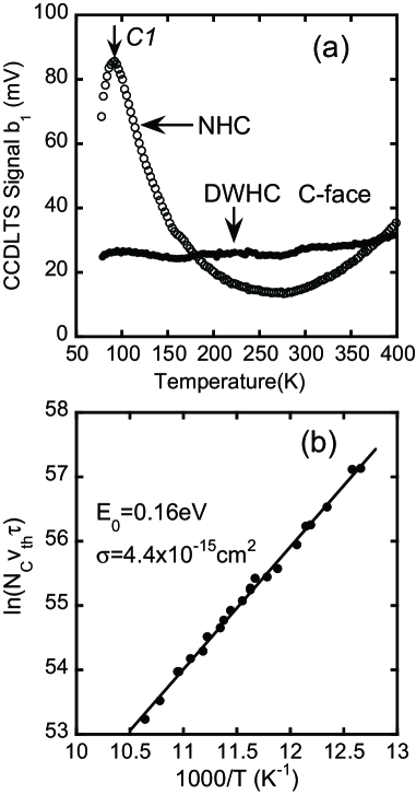
First, we examined the CCDLTS spectra of MOS capacitors on C-face to clarify the cause of the low mobility of the oxynitrided interface T.Hatakeyama et al. (2013). Figure 1 (a) shows the comparison of the CCDLTS spectra between a DWHC sample, the interface of which exhibits a high mobility, and an NHC sample, the interface of which exhibits relatively low mobility. In Fig. 1 (a), the horizontal axis is the first order of the sine coefficient of the DLTFS-signal (b1) with a period width of 205 ms and a recovery time of 4 ms Weiss and Kassing (1988); Weiss (1991). A peak was observed at approximately 100 K in the CCDLTS spectrum for the NHC sample. We refer to this peak as for which an Arrhenius-plot analysis was carried out, and the results was presented in Fig. 1 (b). The obtained energy of the traps that comprise the peak ( traps) was estimated to be 0.16eV. The capture cross-section of the traps was estimated to be 4 10−15cm−2. In contrast, the CCDLTS spectrum for the DWHC sample is almost constant. Especially, the CCDLTS signal at approximately 100 K for the the DWHC sample is one-fourth of that for for the NHC sample. This means that the areal density of traps of the DWHC sample is approximately one-fourth of that of the NHC sample. We conclude that the low mobility in the SiC/SiO2 interfaces fabricated by the NHC process is caused by the high density of traps for the following reasons: (1) the interface mobility is inversely correlated with the density of traps, and (2) the interface mobility degradation mechanism proposed by SaksSaks and Agarwal (2000) can be applied to the high density of traps because the energy level of the traps (0.16 eV) is located above the Fermi energy at the onset of the formation of the inversion layer (approximately 0.2 eV from the edge of the conduction band at room temperature). Consequently, the traps are not filled by electrons at the onset of the formation of the inversion layer; thus some of the inversion electrons are captured when the gate voltage exceeds the threshold voltage, which leads to a degradation in the interface mobility, as described in the introduction.

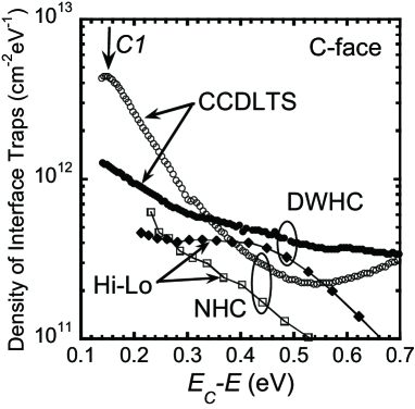
The CCDLTS spectra can be transformed into the energy distribution of the density of the interface traps () with the following two assumptions: (1) depends only weakly on the energy, and (2) the capture cross section does not depend on the energy and temperature. Figure 2 shows the energy distributions for the DWHC and NHC samples calculated from the CCDLTS spectra. In the calculation of , the capture cross sections for the DWHC and NHC samples are assumed to be 410−15cm−2 and 1 10−15cm−2, respectively. For comparison, calculated via the Hi-Lo method are also shown. for the NHC sample steeply increases as the energy become close to the edge of conduction band, whereas that for the DWHC sample gradually increases. As a result, close to the conduction band for the NHC sample is larger than that for the DWHC sample. This large close to the conduction band for the NHC sample corresponds to the traps, and they degrade the MOS mobility for the reason as described above. In contrast, the small close to the conduction band for the DWHC sample results in a relatively large interface mobility of 80 cm2/(Vs).

In Fig. 2, we also present the difference of the energy distributions of characterized from the CCDLTS spectra and those characterized according to the Hi-Lo method Nicollian and Brews (2002), where high-frequency C-V characteristics are measured at 100 kHz. It can be seen that the Hi-Lo method underestimates compared to those estimated from CCDLTS spectra. This is because the frequency of the high-frequency capacitance measurement (100 kHz ) is not high enough to measure the real “high-frequency capacitance” Yoshioka et al. (2012). We note that the interface traps are modeled as a series connection of the resistance and the capacitance in the equivalent circuit of a MOS capacitor Nicollian and Brews (2002). Accordingly, the interface traps have cut-off frequencies. To measure the real “high-frequency capacitance”, the frequency of the C-V measurement should be higher than the cut-off frequency of the traps, which exponentially increases as the energy of traps becomes close to the edge of the conduction band Nicollian and Brews (2002). Therefore, the measured “high-frequency capacitance” is overestimated at the energy close to the edge of the conduction band, which leads to the underestimation of . As for the deep traps ( 0.5 eV), the capacitance measurements tend to be carried out in a non-equilibrium state, which also leads to the underestimation of . As for the NHC sample, the pile up of the nitrogen atoms at the SiC/SiO2 interfaceHaney et al. (2013) may cause a deviation in the estimate of trap energy in the C-V measurements. In summary, the characterization of the SiC/SiO2 interfaces via the Hi-Lo method at room temperature has a numbers of problems; thus, it should be avoided.
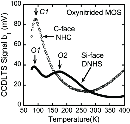
Hereafter, we discuss the difference between the CCDLTS spectrum for MOS capacitors on the C-face and that for MOS capacitors on the Si-face to consider the origin of the traps and other defects at the SiC/SiO2 interfaces. Figure 3 shows a comparison of the CCDLTS spectrum between the oxynitried MOS capacitor on the C-face (the NHC sample) and the one on the Si-face (the DNHS sample). We found two peaks ( and ) in the CCDLTS spectrum for the DNHS sample, as shown in Fig. 3. From an Arrhenius-plot analysis, the energies of the traps and traps are estimated to be 0.14 eV and 0.37 eV, respectively. These peaks were also reported by Basile and his coworkers Basile et al. (2011). It should be noted that the energy of the trap at the SiC/SiO2 interface on the C-face is almost equal to that of the trap on the Si-face. On the other hand, the peak in the CCDLTS spectrum is specific to the SiC/SiO2 interface on the Si-face. The absence of the peak in the CCDLTS spectrum of the SiC/SiO2 interface on the C-face means that the density of traps on C-face is, at least, negligible compared with that of the traps. This information on the dependence of the trap densities on the crystal faces provides an insight into the origin and formation mechanism of traps in the SiC/SiO2 interface.
Here, we review the structure of the SiC/SiO2 interface on the Si-face and C-face. For the SiC/SiO2 interface on the Si-face, uppermost Si atoms, which terminate the SiC layer, are connected to the O atoms in the SiO2 layer Deak et al. (2007); Ohnuma et al. (2007); Devynck et al. (2011a); Devynck (2008); Shen et al. (2013). For the SiC/SiO2 interface on the C-face, it may be reasonable to assume that the uppermost C atoms are connected to the O atoms in the SiO2 layer. However, first-principles molecular-dynamics calculations showed that this interface structure is not stable Ohnuma et al. (2009). Consequently, it is believed that the Si atoms in the SiO2 layer are connected to the uppermost C atoms in SiC Ohnuma et al. (2009); Shen et al. (2013). One of this type of SiC/SiO2 structure was proved to be stable according to first-principles molecular-dynamics calculations Ohnuma et al. (2009). Whatever else it might be, the SiC/SiO2 interface on the C-face may be more unstable than that on the Si-face. This may cause the high oxidation rate of the C-face, which is ten times higher than that of the Si-face Song et al. (2004). Further, the oxidation mechanism may be different between C-face and Si-face Shen et al. (2013). We speculate that the generation of traps on the Si-face may be due to the oxidation mechanism specific to the Si-face.
Basile and his co-workers concluded that the and traps are defects in the oxide on the base of the comparison of CCDLTS spectra between MOS structures on the Si-face of 4H-SiC and those on the Si-face of 6H-SiC Basile et al. (2011). These traps correspond to near-interface oxide traps (NIT), which was first reported by Afanasev and his coworkers in 1997 on the bases of the experiments on phton-stimulated tunneling of trapped electrons (PST) Afanas’ev et al. (1997). Their PST measurements on MOS structures on 4H-SiC and 6H-SiC showed a barrier height of 2.8 eV, which corresponds to an energy for NIT levels at approximately eV, where is the energy of the edge of the conduction band of 4H-SiC. The idea of NIT was also supported by thermally stimulated current measurements using MOS structures on 4H-SiC and 6H-SiC Rudenko et al. (2005). In consideration of these reports, the traps on the C-face, the traps and traps on the Si-face are likely to be oxide traps. Further, the traps on the C-face are likely to be same as the traps on the Si-face because the energy of each of them is almost the same. We presume that the origin of a trap is a carbon dimer or a single carbon defect in SiO2 by comparing the energy of the traps with the charge transition energy of a point defect in SiO2 on the basis of first-principles calculations Deak et al. (2007); Devynck et al. (2011b).

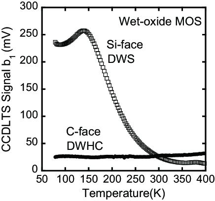
A comparison of CCDLTS spectra of SiC/SiO2 interfaces oxidized in a wet atmosphere on the C-face (a DWHC sample) with that on the Si-face (a DWS sample) is shown in Fig. 4. The CCDLTS spectrum of the DWS sample (Si-face) is much larger than that of the DWHC sample (C-face). This difference in the characteristics of the CCDLTS spectra reflects the difference in interface mobilities between the C-face and the Si-face (DWHC: 80 cm2/(Vs), DWS: 8 cm2/(Vs)). Figure 4 shows that the traps are passivated or removed only on the C-face. If we assume that the trap is an oxide trap, possible mechanisms for the elimination of the traps from the interface can be narrowed down. First, we exclude the possibility of the acceleration of the decomposition of the traps by wet oxidation because the traps could be removed by wet oxidization also on the Si-face if this mechanism works. Therefore, it is natural to think that the difference in the density of the traps between the C-face and the Si-face is due to the difference in the defect-generation rate during wet oxidation. As described above, the structure of the SiC/SiO2 interface on C-face may be totally different from that on Si-face. It is certain that the oxidation mechanism in a wet atmosphere is different between the C-face and the Si-face and that the difference in the oxidation mechanism causes the difference in defect-generation rate at the oxidation front. A more detailed investigation of wet oxidation of SiC from first principles is needed to clarify the mechanism of removal of the traps.
IV Conclusions
We used CCDLTS measurements to characterize and compare close to the edge of the conduction band for SiC/SiO2 interfaces on the Si-face and C-face fabricated using two techniques: oxynitridation and wet oxidation. The results showed that the close to the edge of the conduction band for the SiC/SiO2 interface on the C-face and Si-face fabricated by using oxynitridation was much higher than that on C-face fabricated by using wet oxidation. The high value of close to the edge of the conduction band of oxynitridated samples is due to the traps, which are likely to be the main cause of the low interface mobility. The origin of the traps is likely to be the carbon-related defects in the oxide, which are common in the SiC/SiO2 interfaces on the C-face and Si-face. We found traps in the SiC/SiO2 interface only on the Si-face. We also found that traps in the interface can be eliminated only on the C-face by wet oxidation. It is presumed that the generation of traps in the interface on the Si-face and the elimination of traps in the interface on the C-face by wet oxidation are caused by the oxidation reactions specific to the crystal faces, which are caused by the different atomic structures of the SiC/SiO2 interface between the Si-face and the C-face.
Acknowledgements.
We thank Dr. S. Weiss and Dr. L. Cohausz at Phys Tech GmbH and Dr. H. Okada at Kobelco research, Inc. for their help with DLTS measurements. This research was supported by a grant from the Japan Society for the Promotion of Science (JSPS) through the Funding Program for World-Leading Innovative R &D on Science and Technology (FIRST Program), under the aegis of the Council for Science and Technology Policy (CSTP).References
- Palmour et al. (1993) J. W. Palmour, J. A. Edmond, H. S. Kong, and C. H. Carter, Jr., Physica B 185, 461 (1993).
- Cooper (1997) J. A. Cooper, Jr, Phys. Status Solidi (a) 162, 305 (1997).
- Baliga (2005) B. J. Baliga, Silicon Carbide Power Devices (World Scientific, Singapore, 2005) p. 221.
- Afanas’ev et al. (1997) V. V. Afanas’ev, M. Bassler, G. Pensl, and M. Schulz, Phys. Status Solidi (a) 162, 321 (1997).
- Saks and Agarwal (2000) N. F. Saks and A. K. Agarwal, Appl. Phys. Lett. 77, 3281 (2000).
- Tilak (2009) V. Tilak, Phys. Status Solidi (a) 206, 2391 (2009).
- Dhar et al. (2010) S. Dhar, S. Haney, L. Cheng, S.-R. Ryu, A. K. Agarwal, L. C. Yu, and K. P. Cheung, J. Appl. Phys. 108, 054509 (2010).
- Jamet et al. (2001) P. Jamet, S. Dimitrijev, and P. Tanner, J. Appl. Phys. 90, 5058 (2001).
- Chung et al. (2001) G. Y. Chung, C. C. Tin, J. R. Williams, K. McDonald, R. K. Chanana, R. A. Weller, S. T. Pantelides, L. C. Feldman, O. W. Holland, M. K. Das, and J. W. Palmour, IEEE Electron Dev. Lett. 22, 176 (2001).
- Rozen et al. (2009) J. Rozen, S. Dhar, M. E. Zvanut, J. R. Williams, and L. C. Feldman, J. Appl. Phys. 105, 124506 (2009).
- Nicollian and Brews (2002) E. Nicollian and H. Brews, MOS (Metal Oxide Semiconductor) Physics and Technology (Wiley-Interscience, 2002).
- Suzuki et al. (2009a) T. Suzuki, J. Senzaki, T. Hatakeyama, K. Fukuda, T. Shinohe, and K. Arai, Mat. Sci. Forum 615-617, 557 (2009a).
- Rozen et al. (2010) J. Rozen, X. Zhu, A. C. Ahyi, J. R. Williams, and L. C. Feldman, Mat. Sci. Forum 645-648, 693 (2010).
- Fukuda et al. (2004) K. Fukuda, M. Kato, K. Kojima, and J. Senzaki, Appl. Phys. Lett. 84, 2088 (2004).
- Suzuki et al. (2009b) T. Suzuki, J. Senzaki, T. Hatakeyama, K. Fukuda, T. Shinohe, and K. Arai, Mat. Sci. Forum 600-603, 791 (2009b).
- T.Hatakeyama et al. (2013) T.Hatakeyama, T. Shimizu, T. Suzuki, Y. Nakabayashi, H. Okumura, and T. Kimoto, Mat. Sci. Forum 477-480, 477 (2013).
- Hatakeyama et al. (2005) T. Hatakeyama, T. Watanabe, J. Senzaki, M. Kato, K. Fukuda, T. Shinohe, and K. Arai, Mat. Sci. Forum 483-485, 829 (2005).
- Weiss and Kassing (1988) S. Weiss and R. Kassing, Solid-State Elec. 31, 1733 (1988).
- Weiss (1991) S. Weiss, Halbleiteruntersuchungen mit dem DLTFS-Verfahren, Ph.D. thesis, The university of Kassel (1991).
- Yoshioka et al. (2012) H. Yoshioka, T. Nakamura, and T. Kimoto, J. Appl. Phys. 111, 014502 (2012).
- Haney et al. (2013) S. K. Haney, V. Misra, D. J. Lichtenwalner, and A. Agarwal, Mat. Sci. Forum 707-742, 707 (2013).
- Basile et al. (2011) A. F. Basile, J. Rozen, J. R. Williams, L. C. Feldman, and P. M. Mooney, J. Appl. Phys. 109, 064514 (2011).
- Deak et al. (2007) P. Deak, J. M. Knaup, S. T. Hornos, C. Thill, A. Gali, and T. Frauenheim, J. Phys. D: Appl, Phys. 40, 6242 (2007).
- Ohnuma et al. (2007) T. Ohnuma, A. Miyashita, M. Iwasawa, M. Yoshikawa, and H. Tsuchida, Mat. Sci. Forum 556-557, 615 (2007).
- Devynck et al. (2011a) F. Devynck, A. Alkauskas, P. Broqvist, and A. Pasquarello, Pys. Rev. B. 83, 195319 (2011a).
- Devynck (2008) F. Devynck, First-Principles Study of Defects at the SiC/SiO2 Interface through Hybrid Functionals, Ph.D. thesis, Swiss Federal Institute of Technology in Lausanne (2008).
- Shen et al. (2013) X. Shen, B. R. Tuttle, and S. T. Pantelides, J. Appl. Phys. 114, 033522 (2013).
- Ohnuma et al. (2009) T. Ohnuma, A. Miyashita, M. Iwasawa, M. Yoshikawa, and H. Tsuchida, Mat. Sci. Forum 600-603, 591 (2009).
- Song et al. (2004) Y. Song, S. Dhar, L. C. Feldman, G. Chung, and J. R. Williams, J. Appl. Phys. 95, 4953 (2004).
- Rudenko et al. (2005) T. Rudenko, I. Osiyuk, I. Tyagulski, H. Ö. Ólafsson, and E. Ö. Sveinbjörnsson, Solid-State Electronics 49, 545 (2005).
- Devynck et al. (2011b) F. Devynck, A. Alkauskas, P. Broqvist, and A. Pasquarello, Pys. Rev. B. 84, 235320 (2011b).