Moving boundary and photoelastic coupling in GaAs optomechanical resonators
Abstract
Chip-based cavity optomechanical systems are being considered for applications in sensing, metrology, and quantum information science. Critical to their development is an understanding of how the optical and mechanical modes interact, quantified by the coupling rate . Here, we develop GaAs optomechanical resonators and investigate the moving dielectric boundary and photoelastic contributions to . First, we consider coupling between the fundamental radial breathing mechanical mode and a 1550 nm band optical whispering gallery mode in microdisks. For decreasing disk radius from m to m, simulations and measurements show that changes from being dominated by the moving boundary contribution to having an equal photoelastic contribution. Next, we design and demonstrate nanobeam optomechanical crystals in which a GHz mechanical breathing mode couples to a 1550 nm optical mode predominantly through the photoelastic effect. We show a significant (30 ) dependence of on the device’s in-plane orientation, resulting from the difference in GaAs photoelastic coefficients along different crystalline axes, with fabricated devices exhibiting as high as 1.1 MHz for orientation along the [110] axis. GaAs nanobeam optomechanical crystals are a promising system which can combine the demonstrated large optomechanical coupling strength with additional functionality, such as piezoelectric actuation and incorporation of optical gain media.
I Introduction
Mechanical motion and optical fields are coupled by a number of different mechanisms in cavity optomechanical systems ref:Aspelmeyer_Kippenberg_Marquardt_Review ; ref:Favero_Karrai ; ref:Li_Tang_reactive_coupling ; ref:Wu_Barclay_dissipative_dispersive_OM . Within micro- and nanoscale geometries, perhaps the most commonly considered one is the change in effective optical path length resulting from moving dielectric boundaries, analogous to a movable mirror in a Fabry-Perot cavity. However, the optical path length also depends on the refractive index of the medium filling the cavity, and in solids this can change due to mechanical motion because of the photoelastic effect (electrostriction) ref:Rakich_OE_forces_wgs . This has been observed in stimulated Brillouin scattering in suspended silicon waveguides ref:Rakich_Nat_Comm and cooling and excitation of traveling wave acoustic modes in silica whispering gallery mode resonators ref:bahl2011stimulated . More recently, it has been considered in silicon optomechanical crystals, where optimized geometries that exclusively rely on the photoelastic effect have been developed ref:chan_optimized_OMC .
In this work, we investigate the moving dielectric boundary and photoelastic contributions to the optomechanical coupling in GaAs devices. GaAs has many desirable properties for cavity optomechanics: relatively large photoelastic coefficients ref:Rakich_OE_forces_wgs which can produce devices with high optomechanical coupling ref:chan_optimized_OMC ; piezoelectric properties ref:Masmanidis_Roukes_piezoelectric_Science which can be exploited for driving or readout of mechanical motion; and potential integration with InAs/GaAs quantum dots that offer non-classical light emission and a strong resonant nonlinearity ref:Michler_book_2009 that can be used to probe and control mechanical motion ref:Wilson-Rae ; ref:yeo2013strain .
We first present a combined theoretical and experimental analysis of GaAs microdisks of varying radius, where in large radius devices the moving boundary effect dominates, while in small radius devices the photoelastic effect is the leading contribution. While these trends have recently been theoretically predicted ref:Baker2014photoelastic , here we experimentally demonstrate the importance of considering both these effects in the overall optomechanical coupling rate . We then present two designs of GaAs nanobeam optomechanical crystals that rely predominantly on the photoelastic effect. We show a significant (30 ) dependence of on the in-plane device angle, in contrast with similar Si devices ref:chan_optimized_OMC , for which the dependence is much weaker (3 ). This dependence originates from the much larger magnitude (and opposite sign) of the photoelastic coefficient in GaAs. We experimentally demonstrate this effect by measuring in devices fabricated with differing in-plane angles, and measure as high as 1.1 MHz for devices oriented along the [110] axis of GaAs. Mechanical modes at 2.5 GHz with a quality factor 2000 at room temperature and atmosphere are observed, as is self-oscillation of the mechanical modes through radiation-pressure driven dynamical back-action ref:Kippenberg_Vahala_OE .
II Microdisks
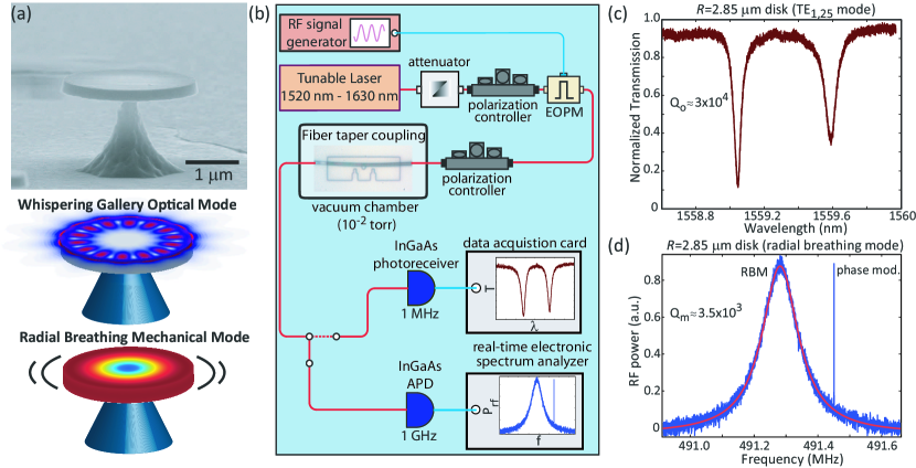
Figure 1(a) shows a scanning electron microscope image of a microdisk cavity fabricated in a 220 nm thick GaAs layer using typical lithography and dry etching processes (see Supplementary Material). Finite-element-method simulations are used to calculate the whispering gallery optical modes and radial breathing mechanical modes of such devices (Fig. 1(a)), with disk radius varying between 1 m and 5 m. For each value of , we calculate optical modes of transverse electric (TE) polarization (dominant electric field components are in the plane of the disk), and determine the azimuthal mode number that places a first order radial mode in the 1550 nm band. We focus on the TE(1,m) mode because of its comparatively high radiation-limited optical quality factor () for small disks ( m). Similarly, we focus on the fundamental radial breathing mechanical mode as it is expected to have a higher mechanical quality factor () than higher-order modes for a given supporting pedestal size.
The optomechanical coupling rate , defined as the optical mode frequency shift due to the mechanical mode’s zero-point motion ref:Gorodetsky_Kippenberg_OM , has moving boundary () and photoelastic () contributions obtained from the calculated modes as in Ref. ref:chan_optimized_OMC :
| (1) | ||||
| (2) |
where is a summation according to the Einstein notation . The are the photoelastic coefficients of GaAs (, , ), is the strain, and is normalized mechanical displacement. Qualitatively, the photoelastic contribution is sensitive to mechanical motion throughout the device, whereas the moving boundary contribution is sensitive to the motion of surfaces (particularly the disk sidewall for the radial breathing mode).
Figure 2 shows the calculated contribution to due to the moving boundary (blue) and photoelastic effects (green) as a function of . For m, the moving boundary effect dominates whereas for m, the photoelastic effect is comparable or even slightly larger. This is consistent with recent simulation results for similar GaAs microdisks ref:Baker2014photoelastic . To verify this scaling behavior experimentally (Fig. 1(b)), we measure fabricated GaAs microdisks of varying radius, following an approach similar to Ref. ref:Gorodetsky_Kippenberg_OM , where a calibration signal of known modulation index from a phase modulator driven close to the mechanical resonance frequency is used to determine the magnitude of (see Supplementary Material). Figure 1(c)-(d) shows representative optical and mechanical modes for a device, where the mechanical mode spectrum also includes the phase modulator calibration tone. Compared to microdisks fabricated previously using an essentially identical process ref:Srinivasan9 , in these devices () is an order of magnitude lower, likely as a result of nm length scale roughness present on the underside of the GaAs layer (see Supplementary Material). Such lower values do not influence the estimate of , but do prevent operation in the sideband-resolved regime needed for a number of applications.
The optomechanical coupling rate can be estimated from a mechanical mode spectrum as (see Supplementary Material):
| (3) |
where is the power in the mechanical mode, is the power in the phase modulator signal, and is the modulation index. , where is the applied voltage and (the voltage required to produce a phase shift) is determined through a separate calibration (see Supplementary Material).
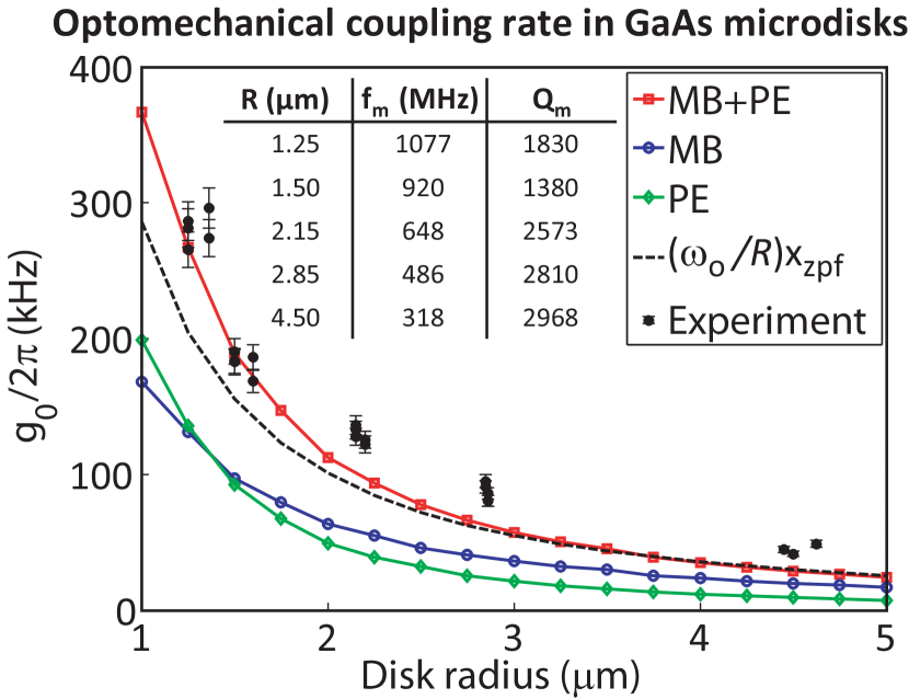
The experimentally measured values for disks of varying are plotted in Fig. 2 (black circles), where the uncertainty in each measurement is dominated by the uncertainty in the phase modulator . The data shows good agreement with the red curve, which plots the sum of the moving boundary and the photoelastic contributions to . Especially for small disk radii, the data shows significant deviation from the moving boundary contribution alone, which might help explain some discrepancies observed in previous measurements of GaAs disk optomechanical resonators, where only moving boundary effects were considered in simulation comparisons ref:Ding_Favero_GaAs_disk_optomechanics . We note that for nominally identical disks, a spread in of is observed. We attribute this to the specifics of the fiber taper coupling for each device, which, we have observed, can perturb the optical and mechanical modes and the resultant optomechanical coupling (see Supplementary Material).
III Nanobeam optomechanical crystals
The measurements of in GaAs microdisks demonstrated that the contribution due to the photoelastic effect () can become comparable to, and even exceed that due to the moving boundary () effect, as the disk radius becomes comparable to the wavelength. Intuitively, as is reduced, the volume of both the optical and mechanical modes decrease and increases due to increased spatial overlap. Given that bending loss starts to dominate for m, one can estimate that kHz based on the data shown in Fig. 2. For higher , one needs to consider geometries that support more tightly confined optical and mechanical modes.
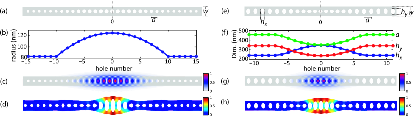
Optomechanical crystals ref:eichenfield2 , structures that spatially co-localize optical modes within a photonic bandgap and mechanical modes within a phononic bandgap, have been demonstrated in a number of materials ref:chan_optimized_OMC ; ref:fan_hong_tang ; ref:Bochmann_Cleland_AlN_uwave_optomechanics ; ref:Davanco_nanobeam_OMC ; ref:kipfstuhl2014modeling ; ref:Phoxonic_crystals_Rolland and in both one- and two-dimensional geometries. Here, we focus on one-dimensional (nanobeam) geometries, where the nanobeams are patterned with a series of holes whose dimensions are graded quadratically from the center (cavity section) to the edge (mirror section). The general design principle for the optical cavity ref:Quan1 relies on choosing the center hole dimension to support a guided mode and then quadratically tapering the hole dimension down to the mirror section where the mode lies in the forbidden band and hence is reflected. The cavity is constructed by putting two such tapers back-to-back. The quadratic taper ensures that the electric field amplitude of the mode has a Gaussian profile and retains high . Similar design concepts have been used in the development of GaAs nanobeam photonic crystal cavities for applications in lasing ref:Gong_Vuckovic_OE_nanobeam and cavity quantum electrodynamics ref:Ohta_cQED_nanobeam . Here, we demonstrate these GaAs cavities in the context of cavity optomechanics, where we note that the tailoring of the hole dimensions also enables localization of mechanical modes ref:eichenfield2 .
Figure 3 shows two different nanobeam optomechanical crystal cavity designs in 220 nm thick GaAs, using circular holes (Fig. 3(a)-(d)) as described above and elliptical holes (Fig. 3(e)-(h)) in an approach similar to Ref. ref:chan_optimized_OMC . For each design, we show a schematic of the geometry, the variation in device parameters as a function of hole number, and the optical and mechanical modes. We designed the devices to have a nominal operating wavelength of 1550 nm and ran a parameter sweep to find designs with the highest , where both moving boundary and photoelastic contributions to are calculated as described earlier for microdisks.
The circular hole design is one realization of the more general elliptical hole design, and is thus comparatively simple in terms of the number of design parameters. In particular, we fix the lattice constant and adjust only the hole radius at the different lattice sites. More specifically, we vary the hole radius in the center of the cavity and the mirror sections, as well as the steepness of the quadratic grading profile (i.e., the number of holes over which the radius is tapered). In comparison, the elliptical hole designs have quadratic grades for the lattice constant () and lengths of the principal axes of the ellipse ( and ). Thus, for each dimension , , and , we vary the value in center of the cavity and mirror sections, as well as the steepness of the quadratic grade.
While for both the circular and elliptical hole designs, we find parameters for which , is higher for the elliptical hole designs. In particular, the optimized elliptical hole design has kHz and kHz for coupling between the nm optical mode and 2.14 GHz mechanical mode, compared to the optimized circular hole design with kHz and kHz for coupling between the nm optical mode and GHz mechanical mode. The elliptical design ensures a higher by having a higher GaAs volume fraction in the center of the beam. We note that while in microdisks, the moving boundary and photoelastic contributions to are comparable in magnitude and of the same sign, for the optimized nanobeams, is dominated by the photoelastic effect and the moving boundary contribution is opposite in sign and thus reduces the net optomechanical coupling rate. This behavior is consistent with Refs. ref:chan_optimized_OMC and ref:kipfstuhl2014modeling , where an optimized nanobeam geometry dominated by the photoelastic effect was developed for Si and diamond, respectively.
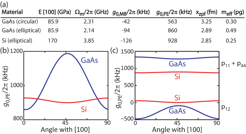
Given that the photoelastic effect is represented by a tensor, one would expect the contribution to to depend on the in-plane orientation of the nanobeam. Moreover, the fact that has a much larger magnitude in GaAs than in Si (, ) suggests that the dependence of on in-plane orientation will be much more significant in GaAs. Figure 4(b) shows for the elliptical hole nanobeam shown in Fig. 3(e)-(h) as a function of the angle the long axis of the nanobeam makes with the [100] direction. The coupling rate is calculated using the rotated photoelastic tensor (see Supplementary Material). We can see that the effect is quite significant with a variation of almost 35 % and a peak value 1.2 MHz at 45 ∘ (device orientation along [110]). We also plot the orientation dependence of for a silicon nanobeam optomechanical crystal similar to that of Ref. ref:chan_optimized_OMC . We see that again, there is a dependence of on in-plane orientation, although in this case the optomechanical coupling rate is minimized at 45 ∘ and the variation between 0 ∘ and 45 ∘ is less than 5 %. To understand this, we plot in Fig. 4(c) the contributions due to the and terms of eqn. 2 as a function of in-plane angle. The in-plane anisotropy of is seen to arise primarily from the contribution due to the term, and the aforementioned difference in the values for GaAs and Si helps us understand why this rotational dependence is so weak in Si. We also point out that the in-plane anisotropy of the elastic coefficients of GaAs leads to an orientation-dependent Young’s modulus ref:brantley_E_fn_angle ; ref:Hopcroft_Youngs_Modulus_Si and a resultant shift in the mechanical mode frequency (see Supplementary Material), but the moving boundary contribution is relatively insensitive to in-plane orientation under the assumption of GaAs being an isotropic elastic material (as can be seen from the form of eqn. 1). The total optomechanical coupling rate for the GaAs elliptical hole design, including both photoelastic and moving boundary contributions, is therefore as high as 1.1 MHz.
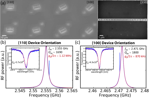
We study this orientation-dependent optomechanical coupling by fabricating a series of GaAs nanobeam devices according to the elliptical hole geometry described above, while varying the orientation of the long axis of the nanobeam between [110] and [100], as shown in Fig. 5(a). Devices are tested in the same measurement setup used to test the microdisk samples (Fig. 1(b)). In this case, the sample is kept at atmospheric pressure, as gas damping is expected to have limited influence on the mechanical modes due to their high frequencies ref:Ekinci_fluid_damping_mechanical_resonators , an effect that has also been observed recently in Si3N4 nanobeam optomechanical crystals ref:Davanco_nanobeam_OMC . Optical modes in the 1550 nm band are observed with typical quality factors (Fig. 5(b)-(c)). The corresponding mechanical mode frequencies vary between 2.555 GHz (alignment along [110]) and 2.471 GHz (alignment along [100]), with the 85 MHz shift resulting primarily from the anisotropy in the Young’s modulus of GaAs (anisotropy in the Poisson’s ratio and shear modulus are also included in simulations; see Supplementary Material). Mechanical quality factors are typically around 103.
Using the phase modulator calibration approach described in Section II, we extract the optomechanical coupling rate for the different devices, with kHz 45 kHz for the device aligned along [100] (Fig. 5(c)) and MHz 0.06 MHz for the device aligned along [110] (Fig. 5(b)). These values correspond reasonably well with simulations, which when taking into account both the photoelastic (Fig. 4(b)) and moving boundary (Fig. 4(a)) contributions, predict kHz and MHz, respectively. Measurement of devices fabricated at an intermediate angle of 15 ∘ with respect to [100] (not shown) yield kHz 50 kHz, respectively, which also matches reasonably well with the simulation result of kHz. We note that while the uncertainty values we have quoted for the measured are the one standard deviation value due to the uncertainty in the phase modulator , another source of uncertainty is in the precise angle with which the cavity was fabricated relative to the GaAs crystal planes (i.e., the alignment of the GaAs chip within the electron-beam lithography system). In particular, for intermediate device orientation angles between [100] and [110], Fig. 4(b) predicts a variation in of 50 kHz for a offset in orientation. We also note that the simulations presented in Fig. 4 assumed that GaAs is an isotropic elastic material, which led to the aforementioned invariance of on in-plane orientation. In the Supplementary Material, we present simulations that treat GaAs as an orthotropic elastic material, and calculate and for orientation along [100] and [110] by rotating the structure within the simulation, rather than using the rotated photoelastic tensor. Since now has some orientation dependence, we find the calculated values for to be a bit closer to the experimental results.
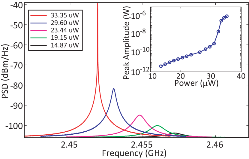
Finally, by injecting increasing levels of optical power into the devices while keeping the laser frequency blue-detuned and on the shoulder of the optical cavity mode, we can drive the system into regenerative mechanical oscillation ref:Kippenberg_Vahala_OE . Figure 6(a) shows a series of mechanical mode spectra for a device oriented along [100], as a function of increasing optical power, from which a clear linewidth narrowing and peak amplitude increase are observed. The peak amplitude is plotted as a function of input optical power in Fig. 6 (b). Here, a characteristic threshold behavior at an input power W is seen, indicating that the system is indeed self-oscillating.
In summary, we have compared the moving dielectric boundary and photoelastic contributions to the optomechanical coupling rate in GaAs optomechanical resonators. Simulations and experiments in microdisk cavities correspond closely and show that these two effects have near equal magnitude for devices with a radius near 1 m. Simulations and experiments on nanobeam optomechanical crystals optimized for photoelastic coupling (one order of magnitude larger than the moving boundary effect) show a significant dependence on the in-plane orientation of the nanobeam, with overall coupling rates MHz achieved for coupling between 1550 nm optical modes and 2.5 GHz mechanical modes.
IV Funding Information
This work was partially supported by the DARPA MESO program. K.C.B. acknowledges support under the Cooperative Research Agreement between the University of Maryland and NIST-CNST Award 70NANB10H193. J.Y.L. and J.D.S. acknowledge support from KIST institutional programs, including the flag-ship, future convergence pioneer, and GRL programs.
V Acknowledgments
We acknowledge J. Kim and S. Krishna from the Center of High Technology Materials at the University of New Mexico for providing epitaxial GaAs material used in fabricating microdisk devices. J.Y.L. is now with the Laser Technology Research Center, Korea Photonics Technology Institute.
References
- (1) M. Aspelmeyer, T. J. Kippenberg, and F. Marquardt, “Cavity Optomechanics,” arXiv p. 1303.0733 (2013).
- (2) I. Favero and K. Karrai, “Optomechanics of deformable optical cavities,” Nature Photonics 3, 201–205 (2009).
- (3) M. Li, W. H. P. Pernice, and H. X. Tang, “Reactive Cavity Optical Force on Microdisk-Coupled Nanomechanical Beam Waveguides,” Phys. Rev. Lett. 103, 223901 (2009).
- (4) M. Wu, A. C. Hryciw, C. Healey, D. P. Lake, H. Jayakumar, M. R. Freeman, J. P. Davis, and P. E. Barclay, “Dissipative and Dispersive Optomechanics in a Nanocavity Torque Sensor,” Physical Review X 4, 021052 (2014).
- (5) P. T. Rakich, P. Davids, and Z. Wang, “Tailoring optical forces in waveguides through radiation pressure and electrostrictive forces,” Opt. Express 18, 14439 (2010).
- (6) H. Shin, W. Qiu, R. Jarecki, J. A. Cox, R. H. Olsson, A. Starbuck, Z. Wang, and P. T. Rakich, “Tailorable stimulated Brillouin scattering in nanoscale silicon waveguides,” Nature Communications 4, 1944 (2013).
- (7) G. Bahl, J. Zehnpfennig, M. Tomes, and T. Carmon, “Stimulated optomechanical excitation of surface acoustic waves in a microdevice,” Nature Communications 2, 403 (2011).
- (8) J. Chan, A. H. Safavi-Naeini, J. T. Hill, S. Meenehan, and O. Painter, “Optimized optomechanical crystal cavity with acoustic radiation shield,” Appl. Phys. Lett. 101, 081115 (2012).
- (9) S. C. Masmanidis, R. B. Karabalin, I. De Vlaminck, G. Borghs, M. R. Freeman, and M. L. Roukes, “Multifunctional Nanomechanical Systems via Tunably Coupled Piezoelectric Actuation,” Science 317, 780–783 (2007).
- (10) P. Michler, ed., Single Semiconductor Quantum Dots (Springer Verlag, Berlin, 2009).
- (11) I. Wilson-Rae, P. Zoller, and A. Imamoḡlu, “Laser cooling of a nanomechanical resonator mode to its quantum ground state,” Phys. Rev. Lett. 92, 075507 (2004).
- (12) I. Yeo, P.-L. de Assis, A. Gloppe, E. Dupont-Ferrier, P. Verlot, N. S. Malik, E. Dupuy, J. Claudon, J.-M. Gérard, A. Auffèves, G. Nogues, S. Seidelin, J.-P. Poizat, O. Arcizet, and M. Richard, “Strain-mediated coupling in a quantum dot-mechanical oscillator hybrid system,” Nature Nanotechnology 9, 106–110 (2014).
- (13) C. Baker, W. Hease, D.-T. Nguyen, A. Andronico, S. Ducci, G. Leo, and I. Favero, “Photoelastic coupling in gallium arsenide optomechanical disk resonators,” Optics Express 22, 14072–14086 (2014).
- (14) T. J. Kippenberg and K. J. Vahala, “Cavity Opto-Mechanics,” Opt. Express 15, 17172–17205 (2007).
- (15) M. L. Gorodetsky, A. Schliesser, G. Anetsberger, S. Deleglise, and T. J. Kippenberg, “Determination of the vacuum optomechanical coupling rate using frequency noise calibration,” Optics Express 18, 23236 (2010).
- (16) K. Srinivasan, M. Borselli, T. J. Johnson, P. E. Barclay, O. Painter, A. Stintz, and S. Krishna, “Optical loss and lasing characteristics of high-quality-factor AlGaAs microdisk resonators with embedded quantum dots,” Appl. Phys. Lett. 86, 151106 (2005).
- (17) L. Ding, C. Baker, P. Senellart, A. Lemaitre, S. Ducci, G. Leo, and I. Favero, “High Frequency GaAs Nano-Optomechanical Disk Resonator,” Phys. Rev. Lett. 105, 263903 (2010).
- (18) M. Eichenfield, J. Chan, R. M. Camacho, K. J. Vahala, and O. Painter, “Optomechanical crystals,” Nature 462, 78–82 (2009).
- (19) L. Fan, X. Sun, C. Xiong, C. Schuck, and H. X. Tang, “Aluminum nitride piezo-acousto-photonic crystal nanocavity with high quality factors,” Applied Physics Letters 102, 153507 (2013).
- (20) J. Bochmann, A. Vainsencher, D. D. Awschalom, and A. N. Cleland, “Nanomechanical coupling between microwave and optical photons,” Nature Physics 9, 712–716 (2013).
- (21) M. Davanço, S. Ates, Y. Liu, and K. Srinivasan, “Si3N4 optomechanical crystals in the resolved-sideband regime,” Appl. Phys. Lett. 104, 041101 (2014).
- (22) L. Kipfstuhl, F. Guldner, J. Riedrich-Möller, and C. Becher, “Modeling of optomechanical coupling in a phoxonic crystal cavity in diamond,” Optics Express 22, 12410–12423 (2014).
- (23) Q. Rolland, M. Oudich, S. El-Jallal, S. Dupont, Y. Pennec, J. Gazalet, J. Kastelik, G. Leveque, and B. Djafari-Rouhani, “Acousto-optic couplings in two-dimensional phoxonic crystal cavities,” Applied Physics Letters 101, 061109 (2012).
- (24) Q. Quan and M. Loncar, “Deterministic design of wavelength scale, ultra-high q photonic crystal nanobeam cavities,” Opt. Express 19, 18529–18542 (2011).
- (25) Y. Gong, B. Ellis, G. Shambat, T. Sarmiento, J. S. Harris, and J. Vuckovic, “Nanobeam photonic crystal cavity quantum dot laser,” Opt. Express 18, 8781 (2010).
- (26) R. Ohta, Y. Ota, M. Nomura, N. Kumagai, S. Ishida, S. Iwamoto, and Y. Arakawa, “Strong coupling between a photonic crystal nanobeam cavity and a single quantum dot,” Appl. Phys. Lett. 98, 173104 (2011).
- (27) W. Brantley, “Calculated elastic constants for stress problems associated with semiconductor devices,” Journal of Applied Physics 44, 534–535 (1973).
- (28) M. A. Hopcroft, W. D. Nix, and T. W. Kenny, “What is the Young’s Modulus of Silicon?” Journal of Microelectromechanical Systems 19, 229–238 (2010).
- (29) D. M. Karabacak, V. Yakhot, and K. L. Ekinci, “High-Frequency Nanofluidics: An Experimental Study Using Nanomechanical Resonators,” Phys. Rev. Lett. 98, 254505 (2007).
SUPPORTING INFORMATION
Fabrication Procedure
The epitaxial material used in the microdisk measurements consists of a 220 nm thick GaAs layer on a 1.5 m thick Al0.6Ga0.4As sacrificial layer. The samples were spin-coated with positive tone electron beam resist and baked at for 2 minutes. The microdisk patterns were exposed in a 100 keV direct write electron beam lithography system with a beam current of 200 pA and nominal dose of 250 C/cm2. After exposure, the electron beam resist was developed using hexyl acetate (65 sec). For improved sidewall roughness, the resist was reflowed at for 1 min. The microdisk patterns were then transferred to the underlying GaAs layer using an inductively coupled plasma reactive ion etcher with an Ar/Cl2 chemistry. The electron beam resist was stripped using trichloroethylene, and the microdisks were undercut with a timed wet etch (depending on the disk radius) using (NH4)2S and dilute HF ref:perahia2009_thesis .
The epitaxial material used in the nanobeam optomechanical crystal measurements consists of a 220 nm thick GaAs layer on a 1.5 m thick Al0.7Ga0.3As sacrificial layer. Device fabrication follows the same general procedure as with the microdisks, with two changes: (1) a slightly higher Cl2 percentage is used in the Ar/Cl2 etch to achieve near-vertical sidewalls in the nanobeam holes, and (2) the devices are undercut with 49 HF.
Gallium Arsenide underside roughness
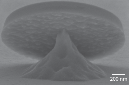
The low optical quality factors measured for the GaAs microdisks in this work () relative to those measured in other work using the same fabrication process ref:Srinivasan9 can be attributed to the presence of significant underside roughness in the GaAs layer which causes additional scattering. The roughness can be seen clearly in Fig. 1, which shows the underside of a collapsed microdisk. The roughness is apparently unrelated to the lithography and dry etching processes, since the underside of the GaAs layer is protected during these stpdf. This suggests that either the wet undercut step, or the initial growth itself, is where the roughness originates. Given the success of the same wet undercut procedure in fabricating similar GaAs devices by many research groups, our current hypothesis is that the roughness arises in the underlying Al0.6Ga0.4As layer, possibly due to temperature variations during growth, and acts as a template for the subsequent GaAs layer growth. This hypothesis is consistent with other reports in the literature ref:sweet2010gaas .
Phase modulator calibration
We use a phase modulator to calibrate the optomechanical coupling rate . The basic idea is to relate the modulation produced by sending light through the cavity optomechanical system (which is driven by its contact with the thermal environment) to a direct phase modulation applied with an electro-optic phase modulator. Because both undergo the same transduction function, as shown by Gorodetsky et al. ref:Gorodetsky_Kippenberg_OM , the ratio of the integrated power in their photocurrent RF spectra will be related to the ratio of and the phase modulator’s modulation index. We go through this derivation below.
The root-mean-square (rms) thermal displacement amplitude () is related to the temperature () using the equipartition theorem:
where is the motional mass of the oscillator and is the mechanical mode frequency. We define a thermal modulation index ref:Eichenfield_thesis :
where the optomechanical coupling parameter () is defined by:
with being the unperturbed cavity frequency. This leads to:
The vacuum optomechanical coupling rate ref:Gorodetsky_Kippenberg_OM is:
where the (rms) amplitude of the zero point fluctuation is:
which can be directly calculated as from the ground state wavefunction of the simple harmonic resonator.
We then relate to :
The modulation index () of the phase modulator is defined as:
where is the signal amplitude and is the modulator half wave voltage.
By comparing the (integrated) powers in the cavity mechanical mode signal and the phase modulator signal obtained from the electronic spectrum analyzer, we get:
Phase modulator Vπ measurement
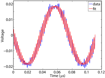
Calibration of the phase modulator is an important step in determining the optomechanical coupling rate using the procedure outlined above. Following the approach and notation described in ref:weis_thesis , we use an unbalanced, fiber Mach-Zehnder interferometer with the phase modulator and input polarization controller placed in one of the arms. The 1550 nm laser is scanned across the interferometer and the transmitted signal is monitored on an oscilloscope that is trigerred with a period corresponding to the laser scan rate. Applying an RF drive to the phase modulator induces modulation sidebands which show up as an amplitude modulation (at the modulation frequency) on the transmitted signal after it passes through the interferometer. The transmitted signal is given as:
| (S1) |
where is a background offset, is the amplitude of the sinusoidal modulation, is the maximum phase modulation which corresponds to the peak voltage of the applied RF signal, is the inverse of the laser scan speed, and is the inverse of the modulation frequency. A nonlinear least squares fit of the transmitted voltage signal from the oscilloscope to eqn. S1 is used to extract . A representative spectrum and fit for a 600 MHz RF signal are shown in Fig. 2, where the = 3.94 V0.2 V. This value is in good agreement with that specified by the vendor datasheet (4 V).
Fiber taper influence on the optomechanical coupling rate
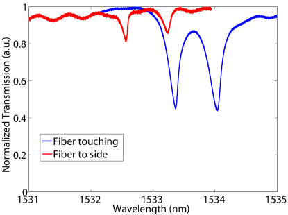
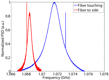
The optomechanical coupling rate in the microdisk is influenced by the presence of the fiber taper waveguide in the near field. Given the high refractive index of GaAs and the accompanying tight mode confinement, the fiber taper waveguide has to be brought in close proximity to the disk to ensure sufficient coupling depth so that one can observe the mechanical modes. This problem is exacerbated in our case by the underside roughness which lowers the intrinsic optical of the cavities significantly. If the fiber taper comes in contact with the disk, it perturbs both the optical mode (by modifying the field distribution) and the mechanical mode (by clamping the motion where the fiber touches the disk). This can be seen by a shift in the resonance wavelength of the disk in both the optical (Fig. 3) and mechanical mode spectra (Fig. 4) as well as an increase in the corresponding damping rates. We find that the extracted coupling strength for devices in which the fiber taper has come into contact with the microdisk can be significantly different ( in some cases) than those in which the fiber is held to the side of the disk. For the measurements shown in Fig. 2 in the main text, we have attempted to keep the fiber taper waveguide coupling position consistent for all of the measured microdisks, with the coupling depth (extinction ratio 75 %) of the optical mode and the mechanical Q ( 1000) of the radial breathing mode mode serving as consistency checks for disks of the same nominal diameter.
Finally, we note that while our work has assumed that the inferred optomechanical coupling rate is purely due to dispersive coupling (consisting of both moving dielectric boundary and photoelastic components), recent work has highlighted the potential for other coupling mechanisms, such as dissipative coupling in which the intrinsic and extrinsic quality factors of the optical cavity depend on the motion of the mechanical resonator ref:Wu_Barclay_dissipative_dispersive_OM . These authors have found that the fiber taper waveguide can influence the magnitude of both the dissipative and dispersive optomechanical coupling rates ref:Hryciw_Barclay_arXiv .
Optomechanical coupling for the TE2,m microdisk mode
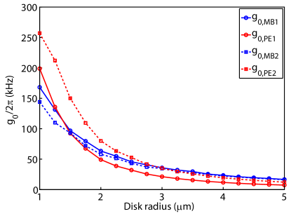
We have also considered the moving boundary and photoelastic components to the optomechanical coupling rate between the TE2,m whispering gallery mode and radial breathing mechanical mode in GaAs microdisks. Simulation results are shown in Fig. 5. For comparison, we also plot the corresponding values for the TE1,m mode. As can be seen, the moving boundary contribution to remains comparable for the two modes but the photoelastic contribution for TE2,m is greater than that for the TE1,m mode. Since the photoelastic contribution roughly scales as , the higher coupling for the TE2,m can be attributed to greater overlap between the electric field and the displacement in the interior of the disk. In practice, we did not look for TE2,m due to their relatively low radiation-limited optical quality factors for the smallest diameter disks.
Silicon nanobeam optomechanical crystal design
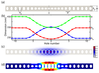
The schematic, beam parameters, normalized electric field amplitude of the optical mode, and normalized mechanical mode displacement of the Si nanobeam design discussed in Fig. 4 in the main text is shown in Fig. 6. The Young’s modulus, density and refractive index values used were 170 GPa, 2329 kg/m3, and 3.48 respectively. The nanobeam design is based on Chan et al. ref:chan_optimized_OMC .
Rotated photoelastic tensor
The rotated photoelastic tensor can be constructed following ref:chan2012_phd ( subscript indicates component in rotated frame, is the in-plane rotation angle from [100] ):
The term can be constructed as:
and the perturbation can be calculated as:
Breathing mode simulation with aniostropic elastic constants
The elastic anisotropy of GaAs (, and (in units of Pa) ref:brantley_E_fn_angle ; ref:Hopcroft_Youngs_Modulus_Si leads to an orientation-dependent Young’s modulus (inset of Fig. 7), Poisson’s ratio, and shear modulus, and a corresponding orientation dependence of the nanobeam mechanical breathing mode frequency. Figure 7 shows this dependence, where a frequency shift of 100 MHz is expected between devices oriented along [100] and [110]. This corresponds reasonably with the measured frequency shift of 85 MHz.
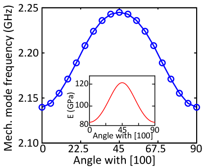
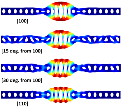
For calculating the breathing mode frequency as a function of in-plane angle, GaAs was represented as an anisotropic material using an orthotropic elasticity matrix with parameters = 121.2 GPa, = 121.2 GPa, = 85.9 GPa, = 0.0209, = 0.4434, = 0.312, = 32.5 GPa, = 59.4 GPa, and = 59.4 GPa. The values used here correspond to the x-axis along [110]. The beam is physically rotated about the z-axis to calculate the breathing mode frequency as a function of in-plane angle. Figure 8 shows the displacement profile for the breathing mode for 0 ∘, 15 ∘, 30 ∘, and 45 ∘ from the [100] axis. For 15 ∘ and 30 ∘, the displacements are no longer symmetric (as can be seen from the distorted hole shapes) and the mechanical mode confinement is reduced. As a general rule of thumb, designs along [110] or [100] are expected to give the highest mechanical Q.
Dependence of the moving boundary contribution on in-plane orientation
The rotation dependent shown in Fig. 4 in the main text was calculated assuming GaAs was an isotropic material ( = 85.9 GPa, =0.31, ) and rotating the photoelastic tensor. For an isotropic material, is independent of in-plane orientation as can be seen from the form of eqn. 1 in the main text.
For completeness, we calculated and for nanobeams simulated with GaAs as an orthotropic elastic material (with mode shapes shown in Fig. 8). For calculating the overlap integrals along [100], we rotated the nanobeam by 45 ∘ and solved for the optical mode. As expected from the different breathing mode profiles, is different along [100] ( kHz) and [110] ( kHz). The total along [100] ( 850 kHz) and [110] ( 1.06 MHz) are within ten percent of the values reported in Fig. 4(a) in the main text, on account of being dominated by the photoelastic effect.
References
- (1) R. Perahia, “Investigation and application of microscale semiconductor lasers and cavities,” Ph.D. thesis, California Institute of Technology (2009).
- (2) K. Srinivasan, M. Borselli, T. J. Johnson, P. E. Barclay, O. Painter, A. Stintz, and S. Krishna, “Optical loss and lasing characteristics of high-quality-factor AlGaAs microdisk resonators with embedded quantum dots,” Appl. Phys. Lett. 86, 151106 (2005).
- (3) J. Sweet, B. Richards, J. Olitzky, J. Hendrickson, G. Khitrova, H. Gibbs, D. Litvinov, D. Gerthsen, D. Hu, D. Schaadt et al., “Gaas photonic crystal slab nanocavities: Growth, fabrication, and quality factor,” Photonics and Nanostructures-Fundamentals and Applications 8, 1–6 (2010).
- (4) M. L. Gorodetsky, A. Schliesser, G. Anetsberger, S. Deleglise, and T. J. Kippenberg, “Determination of the vacuum optomechanical coupling rate using frequency noise calibration,” Optics Express 18, 23236 (2010).
- (5) M. Eichenfield, “Cavity optomechanics in photonic and phononic crystals: Engineering the interaction of light and sound at the nanoscale,” Ph.D. thesis, California Institute of Technology (2010).
- (6) S. A. Weis, “Cavity-optomechanics with silica microtoroids: Quantum-coherent coupling and optomechanically induced transparency,” Ph.D. thesis, Ecole Polytechnique Federale de Lausanne (2012).
- (7) M. Wu, A. C. Hryciw, C. Healey, D. P. Lake, H. Jayakumar, M. R. Freeman, J. P. Davis, and P. E. Barclay, “Dissipative and Dispersive Optomechanics in a Nanocavity Torque Sensor,” Physical Review X 4, 021052 (2014).
- (8) A. C. Hryciw, M. Wu, B. Khanaliloo, and P. E. Barclay, “Near-field tuning of optomechanical coupling in a split-beam nanocavity,” (2014).
- (9) J. Chan, A. H. Safavi-Naeini, J. T. Hill, S. Meenehan, and O. Painter, “Optimized optomechanical crystal cavity with acoustic radiation shield,” Appl. Phys. Lett. 101, 081115 (2012).
- (10) J. Chan, “Laser cooling of an optomechanical crystal resonator to its quantum ground state of motion,” Ph.D. thesis, California Institute of Technology (2012).
- (11) W. Brantley, “Calculated elastic constants for stress problems associated with semiconductor devices,” Journal of Applied Physics 44, 534–535 (1973).
- (12) M. A. Hopcroft, W. D. Nix, and T. W. Kenny, “What is the Young’s Modulus of Silicon?” Journal of Microelectromechanical Systems 19, 229–238 (2010).