Novel Differential Conductance Oscillations in Asymmetric Quantum Point Contacts
Abstract
Small differential conductance oscillations as a function of source-drain bias were observed and systematically studied in an asymmetric quantum point contact (QPC). These oscillations become significantly suppressed in a small in-plane magnetic field () or at higher temperatures (). Qualitatively, their temperature evolution can be simulated numerically based on smearing of the Fermi distribution, whereas features near zero-bias cannot. Single particle scenarios are unsatisfactory in accounting for the oscillations, suggesting that they are likely caused by electron and spin correlation effects.
pacs:
73.63.-b,73.63.NmAfter years of search, the elusive quantum Wigner crystal-like state in 1-dimension and quasi-1-dimension, a state in which an uncertainty in the momentum yields a relevant kinetic energy scale, but Coulomb repulsion wins out–still has not been unequivocally demonstrated. The most promising system, in which a systematic study can be carried out using transport measurements, is the QPC system. Despite the lack of a smoking-gun signature, such as a threshold for conduction analogous to the motion of a pinned charge density wave (or at least a highly nonlinear increase beyond some pinning voltages), to date, several puzzling characteristics have been discovered in ballistic QPCs, when the number of conduction channels (transverse modes) is tuned toward the single channel limit. These include the well-studied 0.7 anomaly Thomas ; Micolich , the suppression (or destruction) of the first quantized conductance plateau, HewPepper1 ; HewPepper2 ; Wu ; Hao as well as higher plateaus HewPepper2 ; Hao_thesis , and the recently discovered conductance resonances in geometrically asymmetric QPCs Wu ; Hao . None of these features can be explained adequately without introducing Coulomb interaction and spin effects.
In this letter, we report the discovery of a new signature unique to the QPC system. Specifically, we focus on unusual oscillations in the differential conductance () as a function of source-drain bias, in an asymmetric ballistic QPC. The magnetic field behavior shows that these oscillations are readily suppressed under a small in-plane magnetic field (), while the temperature dependence shows that these oscillations are washed out at around . This type of oscillations as a function of source-drain bias has not been reported in the published literature in any electronic system Liu2009Brun2014 ; the only possible exception is unpublished work in a quadruple-quantum-dot, which is entirely different from the QPC system Shang2013 . Similar oscillations are reproduced is a second sample at and zero magnetic field. It is noteworthy that in the quadruple quantum dot (QD) system–arranged in two rows of double-QDs, the oscillations, at least two (and up to four) to each side of zero bias, were likely of a Kondo origin. This raises the possibility that in our QPC system, Kondo physics is involved, which arises when the electron system spontaneously forms a double-row of localized puddles, suggestive of a double row lattice.
Our QPC samples were fabricated by electron beam lithography, evaporation of the Cr/Au surface gates and lift-off. The two-dimensional electron gas (2DEG) is located at a shallow depth 85 nm below the surface of the GaAs/AlGaAs heterostructure crystal. The carrier density and mobility are and respectively, giving a mean free path . An excitation voltage at 17.3 Hz was applied, and the current was measured in a PAR124A lock-in amplifier after conversion to a voltage using a home-made current preamplifier. The measurement was first carried out in a He-3 fridge with a base temperature , and then repeated in a dilution refrigerator with a base temperature below . All data shown in this paper are qualitatively reproducible with thermal cycling.

Before presenting the main data for the oscillations in the 100 nm channel length, asymmetric QPC, we begin by addressing the issue of donor/impurity-induced disorder in our QPC devices. To establish with confidence that what we observe are intrinsic effects, and not from disorder, we contrast the behavior of the linear conductance in an asymmetric QPC, against symmetric QPCs with smooth and gradual entrances and exits. Fig. 1 shows the linear conductance for both symmetric (left panels) and asymmetric QPCs (right panels). Symmetric QPCs have two geometrically symmetric split gates while the asymmetric ones were fabricated by replacing one split gate with a long gate. This long gate is labeled the wall gate while the other short gate labeled the finger gate. The scanning electron microscope images of asymmetric QPCs can be found in Ref. Wu ; Hao . The left two figures in Fig. 1 show the linear conductance for two symmetric QPCs with different channel lengths (100 nm and 500 nm respectively), while the right two figures for one asymmetric QPC at and at , respectively. The data in Figs. 1(b) and (d) for the 100 nm asymmetric QPC are from different cool downs. During measurement, the wall gate voltage for the asymmetric QPC () was held fixed, while the gate voltage was scanned to measure the conductance.
In our previous work Hao , conductance resonances and their behavior versus channel length were reported. The dirt effects, caused by dopant impurity and lithographic imperfections, were largely ruled out. Here using the symmetric QPCs as a control group, we present more clear-cut evidence to rule out dirt effects. (The supplementary document supplement contains an expanded discussion.) Especially for Fig. 1(c), in a symmetric QPC with a long, channel length, almost no conductance resonances are observed down to 300mK (except for the 0.7 effect Thomas ). While for the long asymmetric QPC fabricated on the same crystal, dense conductance resonances are observed (in Fig. 2 (c) of Ref. Hao ). If the resonances in asymmetric QPCs were caused by dirty effects, then the symmetric QPCs (Fig. 1(a)(c)) should also show dirt-induced resonances. The absence of resonances in the symmetric QPCs other than the quantized plateaus clearly rules out impurity effects. Thus, the resonances are indeed intrinsic, which as ascribed, are due to electron correlations. Besides resonances, modulation of conductance plateaus was also observed in asymmetric QPCs.Wu ; Hao The symmetric QPCs with smoothed entrance/exit (Fig. 1(a)(c)) show no plateau modulation as the was tuned from the left most to the right most, e.g. the value of plateau remains at the quantized value throughout, while for the asymmetric QPC (Fig. 1(b)(d)), clear modulation of the first and second quantized plateaus are observed. The dotted lines mark the quantized plateaus positions.
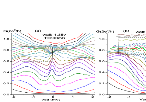
Fig. 2 shows the as a function of source drain bias (), for the asymmetric QPC (corresponds with Fig. 1(b)(d)), at (a) and (b) for different cool downs. Unusual small oscillations, which have not previously been reported in QPCs, are developed. Several typical oscillations are highlighted in the regions enclosed by the black dashed rectangular boxes. We will focus on the systematic study of these oscillations in the remainder of this manuscript.
The measurement was configured in the following way: during the measurement, was held fixed, while was varied for different individual curves (different colors online). in Fig. 2(a) was set at the same value as the rightmost red curve in Fig. 1(b), while Fig. 2(b) has the same value as the leftmost red curve in Fig. 1(d). The curves, corresponding with other red linear curves of Fig. 1(b)(d), were also systematically measured. These additional curves show very similar behavior with those presented in this paper (including their magnetic field and temperature dependence). The three linear red curves in Fig. 1(b) or (d) represent three linear conductance regions, which alternately exhibit a weak, strong and then weak first quantized plateau. The consistency of the three sets corresponding with the red linear curves in Fig. 1(b) or (d) for different cool downs, suggests that the oscillations exist in a wide gate voltage range. For each trace, was swept back and forth at different speeds between and . The inset in Fig. 2 contains the back and forth sweeping for one typical curve to demonstrate reproducibility.
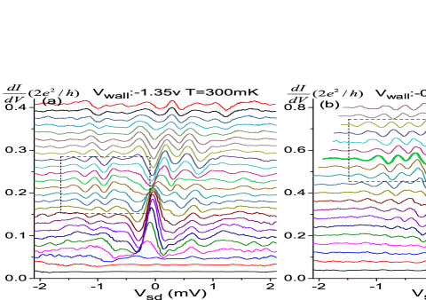
To highlight these oscillations, a smoothed background was subtracted. The background was generated by smoothing over a relatively wide range to average out the small oscillations (the thin red curve, passing through the thick green curve in Fig. 2(b), represents a typical smoothed background of the thick green curve). Fig. 3 shows the curves after background subtration, offset for clarity. (Note that the thick green curve in Fig. 3(b) corresponds with the thick green curve in Fig. 2(b) after subtracting the red curve). A typical curve has around oscillations. A typical oscillation amplitude at is roughly . At , the oscillation size is roughly halved, as indicated by a comparison of the oscillations in the dashed rectangular boxes in Figs. 3 (a) and (b), where the vertical scale for (b) is twice as for (a). The separation between neighboring oscillations is in at and at .
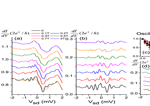
Fig. 4(a) shows the in-plane magnetic field dependence of a typical trace. Different magnetic fields are represented with different colors. The curves in Fig. 4(b) correspond with those in (a) with the smoothed background subtracted. Fig. 4(d) shows the in-plane magnetic field dependence for a second set of fixed and values, (also with smoothed background subtracted). Figs. 4(b)(d) indicate that at a low in-plane magnetic field (), the oscillation sizes are already significantly reduced, and are nearly fully suppressed by . This surprising in-plane magnetic field behavior is systematically characterized and examined below.
The magnetic field dependence of nine traces were measured to obtain reasonable statistics. These nine sets were chosen in the following way: for each red curve in Fig. 1(d), the magnetic field dependence of three traces, corresponding with three different settings, were measured. Fig. 4(b) and (d) represent two of the nine sets. Fig. 4(c) shows a summary for the nine sets, providing a general trend of how the average oscillation size evolves with in-plane field. The average oscillation size was calculated in the following way: for each curve at a specific magnetic field, after subtracting the smoothed background, the average oscillation size was estimated by calculating the average absolute value for all data points of this new curve. Then we normalize the size against the size of each curve at . For each field, there are nine red dots (some not visible) representing the average oscillation amplitude of each of the nine curves, while the black dot represents the mean value of the nine red dots. The fact that the oscillation amplitude does not decay fully to zero may be due to non-zero contributions not related to the oscillations, such as noise. Another method, based on the average root-mean-square, instead of the average absolute value, showed similar trends as Fig. 4(c). At , the mean oscillation size (black dot) of these nine curves is nearly saturated in its decay trend.
In Fig. 4(a), the orange curve overlapping the black curve (B=0 T), is identical with the upper orange curve (B = 0.7 T), but without offset. The orange curve, for which the oscillations are nearly suppressed, passes through the black curve for the most part. This behavior is found for all the other traces: these curves with reduced oscillations pass through the B=0 T curves, when plotted without vertical offset. This behavior will be discussed in the supplemental document supplement as one evidence to rule out the weak/anti-weak localization scenario. If we were to assume a typical g-factor of , the Zeeman energy scale would be , a factor of three smaller than than the oscillation separation() even at . We emphasize that the sensitivity to such a small in-plane B field () is highly unusual and completely unexpected!
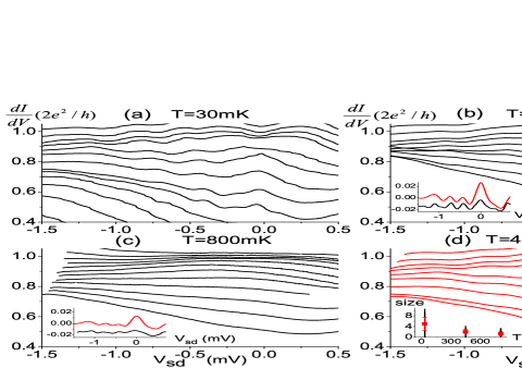
Fig. 5 shows the temperature evolution of these oscillations, for which the corresponds to the middle red linear conductance curve in Fig. 1(d), at (a), (b) and (c). The oscillations become smaller at higher temperatures and are almost washed out at . The temperature evolution of the oscillations, corresponding to the right and left red curves in Fig. 1(d), show consistency with Fig. 5. The in Fig. 5(a) is held fixed at , while at higher temperatures(, ), due to drift, and by comparing the linear conductance traces, was fixed at in Figs. 5(b) and (c).
Fig. 5(d) shows the numerical simulation of the at , which qualitatively agrees with the measured data in Fig. 5(b). The simulation, based on thermal broadening of the Fermi distribution, involves convoluting the transmission probability with the Fermi function to deduce the conductance at higher temperatures, as discussed in the supplemental document supplement .
To better compare the measured oscillations with the simulation at each temperature, in the insets in Fig. 5(b)(c), we show the after subtracting the smoothed background, for one representative trace in Fig. 5(b) or (c). By comparing the measured data (black) and the simulated ones (red) at and in the inset of (b)(c), the oscillation sizes are seen to be semi-quantitatively in agreement, for the oscillations off zero bias. However, the structure at zero bias does not agree with, and is obviously smaller than, the simulation results. This difference in behavior suggests that the two bias regions may have different energy scales and thus are related to different origins, e.g. multi-Kondo scales or a new mechanism. In such a Kondo scenario, it is still single channel physics, as opposed to 2- or higher channel. Thus, the behavior should still be Fermi-liquid-like.
The inset in Fig. 5(d) shows the statistics for the average oscillation size of every curves at different temperatures. This statistics provides a trend of how the oscillation sizes decreases as increasing the temperatures. The oscillations are almost washed out at . The corresponding thermal energy scale, is , , and , respectively. The average oscillation size is calculated using the same method discussed in the statistics of magnetic field dependence. At a given temperature, the black vertical line indicates the spread in the average oscillation size for individual curves at a particular gate voltage, while each red dot is the mean value of all curves contained within the black line.
In the above, we have provided a fairly complete characterization of the oscillations. At present, there does not exist any theory, which can be used to interpret the unusual oscillations, although a high-spin Kondo effect reflecting an underlying electron lattice represents an important possibility. Several possibilities that may arise within simple single particle scenario are considered in the supplemental document and ruled out supplement , due to the fact that the size of the oscillations and its magnetic field dependence behavior do not agree with any of these models: for example, the contribution from the 2DEG reservoir can only give rise to an oscillation with a size much smaller than measured. Thus the oscillations are from the QPC channel. The possible excitation to quasi-bound states, modulation of energy bands due to magnetic field, field misalignment, Aharonov-Bohm effects and weak or anti-weak localizations, are also carefully considered, but are inconsistent with the data (and its magnetic field dependence).
By virtue of having ruled out all sensible single particle pictures, we are led to the conclusion that our observation must be related to electron-electron interactions. Since an in-plane magnetic field mainly interacts with electron spin, the magnetic field dependence suggests that the small oscillations are related to electron spin correlation. Based on the estimated 1D electron density in the single channel limit Wu_thesis , a rough estimate of the electron number inside the QPC channel is around , which is of the same order as the number of oscillations for a typical curve. In future studies, it will be interesting to directly relate such oscillations to the formation of localized charge state inside the QPC channel due to correlation effects, possible of relevance to the exotic zigzag type of Wigner-crystal-like states Matveev ; Abhijit , for instance, via the manifestation of a high spin Kondo state, reflection an underlying lattice of spontaneously formed, localized electron array.
We thank M. Melloch for the GaAs/AlGaAs crystal. This work was supported in part by NSF DMR-0701948, and by the Academia Sinica, Taipei.
References
- (1) K. J. Thomas, J. T. Nicholls, M. Y. Simmons, M. Pepper, D. R. Mace, and D. A. Ritchie, Phys. Rev. Lett. 77, 135 (1996).
- (2) A. P. Micolich, Journal of Physics: Condensed Matter 23, 443201 (2011).
- (3) W. K. Hew, K. J. Thomas, M. Pepper, I. Farrer, D. Anderson, G. A. C. Jones, and D. A. Ritchie, Phys. Rev.Lett. 101, 036801 (2008).
- (4) W. K. Hew, K. J. Thomas, M. Pepper, I. Farrer, D. Anderson, G. A. C. Jones, and D. A. Ritchie, Phys. Rev. Lett., 102, 056804 (2009).
- (5) P. M. Wu, Peng Li, Hao Zhang, and A. M. Chang, Phys. Rev. B 85, 085305 (2012).
- (6) H. Zhang, P. M. Wu, and A. M. Chang, Phys. Rev. B 88, 075311 (2013).
- (7) It appears that a similar type of oscillations may be present in two works: Figure 2 in Liu et al, PhysRevB.81.235316, 2010. and Figure 1 in Brun et al, Nature Communication 5290, 2014. Although the authors did not mention that in their respective papers.
- (8) Runan Shang et al., arXiv:1312.2376 version 2.
- (9) Hao Zhang, PhD Thesis, Duke University (2014).
- (10) Hao Zhang, Phillip M. Wu, and A.M. Chang, supplemental document to this manuscript.
- (11) Phillip M Wu, PhD Thesis, Duke University (2010).
- (12) A. D. Klironomos, J. S. Meyer and K. A. Matveev, Europhysics Letters 74, 679 (2006).
- (13) A. C. Mehta, C. J. Umrigar, J. S. Meyer, and H. U. Baranger, Phys. Rev. Lett. 110, 246802 (2013).