Magnetisms in -type monolayer gallium chalcogenides (GaSe, GaS)
Abstract
Magnetisms in -type monolayer GaX (X=S,Se) is investigated by performing density-functional calculations. Due to the large density of states near the valence band edge, these monolayer semiconductors are ferromagnetic within a small range of hole doping. The intrinsic Ga vacancies can promote local magnetic moment while Se vacancies cannot. Magnetic coupling between vacancy-induced local moments is ferromagnetic and surprisingly long-range. The results indicate that magnetization can be induced by hole doping and can be tuned by controlled defect generation.
pacs:
75.50.Pp, 71.15.Mb, 61.72.JiI Introduction
The researches of two-dimensional (2D) materials have attracted extensive interest recently. A varieties of 2D crystals have been discovered which exhibit remarkable properties. These include grapheneNovoselov2004 ; Novoselov2005 ; Zhang2005 ; Geim2007 , a gapless semiconductor, single-layer boron nitrideKim2012 ; Tusche2007 , a wide-gap insulator, and monolayer transition metal dichalcogenides, a class of direct band-gap semiconductor with excotic spin and pseudospin physicsXiao2012 ; Wang2012 ; Splendiani2010 ; Mak2010 . Semiconducting 2D crystals are of interest as the next generation host materials for future electronic applications exploiting internal degrees of freedom of carriers such as spin in addition to the chargeXu2014 . An indispensible element of spin based electronics is magnetism which can play the role of non-volatile memory. Realizing robust magnetic semiconductor has been a long term effort in the exploration of semicondutor-based spintronicsWolf2001 . The conventional approach to introduce magnetism in semiconductors is by doping transition metal elementsOhon1998 ; Dietl2000 ; Jungwirth2006 . Recently, unexpected high-temperature ferromagnetism have been reported in systemsMonnier2001 ; Elfimov2002 ; Venkatesan2004 ; Pan2007 ; Dev2008 ; Peng2009 , which do not involve the partially occupied or orbitals. In carbon structures, first-principles calculations have also shown that magnetism can be induced by nonmagnetic defectsKusakabe2003 ; Kim2003 ; Chan2004 ; Andriotis2006 . While the origin of magnetism in these systems is not well understood, the large density of states at the band edge is considered to be the key for several materialsPeng2009 , which implies a new possibility for searching spintronic materials. In 2D crystals like BN, graphene and MoS2, first-principle calculations have also predicted that local magnetic moment can be induced by nonmagnetic impurities or vacanciesLiu2007 ; Yazyev2007 ; Zhang2007 ; Zhou2013 .
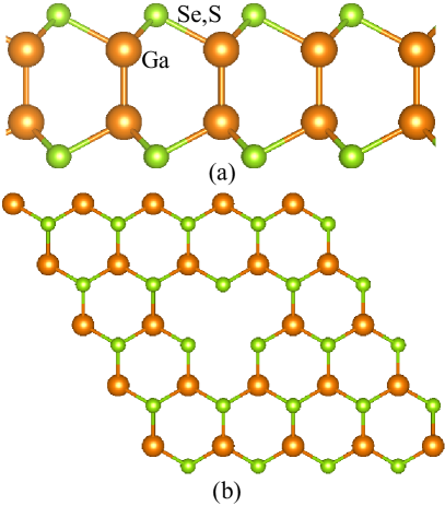
GaSe and GaS are stable layered semiconductors, formed by vertically stacked X-Ga-Ga-X sheets held together by van der Waals interactions, as shown in Fig. 1(a). They have attracted considerable interest because of their remarkable nonlinear optical propertiesSegura1997 ; Nusse1997 ; Kato2011 . Very recently, ultrathin GaS and GaSe nanosheets have been synthesized and experimentally studiedHu2012 ; Late2012 . Zolyomi et al. have performed first-principles calculations of GaX monolayers and found a sombrero dispersion near the top of the valence bandZolyomi2013 , which gives rise to a large density of states at the valence band edge (VBE). Therefore, monolayer GaX can be a promising system to explore ferromagnetism in the 2D limit.
In this manuscript, we investigate the magnetism in hole-doped GaX monolayers using density functional theory calculations. We find that GaX monolayer becomes ferromagnetic with a small range of hole doping. In this range, the polarization energies first increases then decreases to zero. Under Se-rich condition, a Ga vacancy is more favorable, rendering the GaSe intrinsic type. A S vacancy can be spontaneously introduced and makes GaS intrinsic type. These are in agreement with the experimentLate2012 . The intrinsic Ga vacancies can promote the formation of local magnetic moments. We also find that the magnetic coupling between these defects is ferromagnetic and surprisingly long-ranged.
II Electronic structures and hole-induced magnetism of monolayer GaSe and GaS
II.1 Computation method
Our density functional theory (DFT) calculations employ the projector augmented wave (PAW) method encoded in Vienna ab initio simulation package(VASP) Kresse1993 ; Kresse1996 ; Kresse1996B , and the generalized-gradient approximation (GGA) for the exchange correlation functional Perdew1996 is used. Throughout this work, the cutoff energy of 400 eV is taken for expanding the wave functions into plane-wave basis. The calculated lattice constants for monolayer GaSe and GaS are 3.817 and 3.627 Å, respectively. A centered k-point grids are used to sample the Brillouin zone for the primitive cell. In the hole doping calculation, k-point grids are adopted. For the vacancy calculation, we adopt supercell to simulate the system with defects, which is large enough to avoid the interaction between the defects. A set of centered k-points is used for the defect calculation. A 15 Åvacuum layer is used in our calculation to avoid interaction between slab. The convergence for energy is chosen as eV between two steps and the maximum Hellmann-Feynman force acting on each atom is less than 0.02 eV/Åupon ionic relaxation for decfect calculation( 0.01 eV/Åfor primitive cell GaX).
The formation energy of neutral vacancies in monolayer GaSe or GaS, , is defined as,
| (1) |
where is the total energy of monolayer GaSe or GaS with Y (Y=Ga, Se, S) vacancies. is the energy of pristine monolayer GaSe or GaS and refers to the chemical potential of detached X atom. is obviously environment dependent. We consider two cases: Ga-rich and Se-rich or S-rich. In Ga-rich environment, is calculated from orthorhombic Ga crystal and , where () is the chemical potential of a GaSe (GaS) unit in 2H-GaSe (2H-GaS) crystal. In Se-rich or S-rich environment, () is calculated from hexagonal Se (orthorhombic S) crystal and .
II.2 Electronic structures and hole-induced magnetism for Monolayer GaSe and GaS
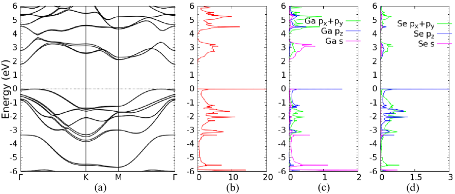
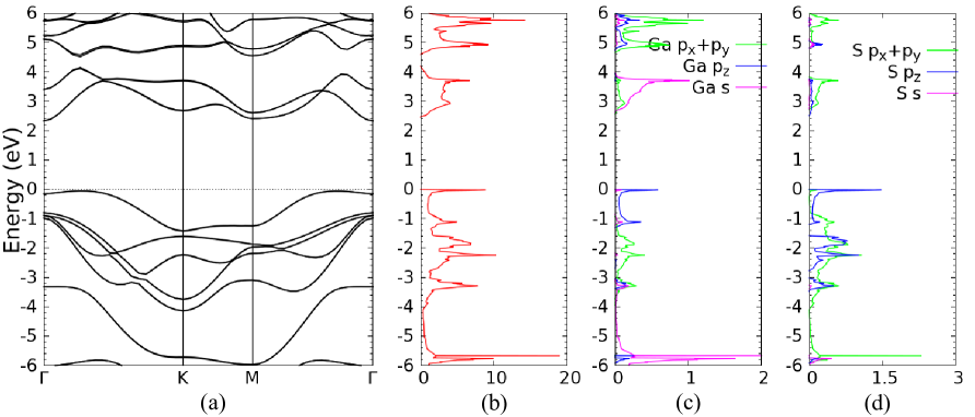
The band structures of monolayer GaSe and GaS with spin orbit coupling are presented in Fig. 2 and Fig 3, respectively. Both monolayer GaSe and GaS are semiconductors with indirect bandgaps, which are just slightly lower than the direct bandgaps. The bandgaps of monolayer GaSe and GaS are 2.1 eV and 2.5 eV, repsectively. The bottom of the conduction band is mainly attributed to Ga orbital, hybridized with and orbitals of X (X=Se, S). The top of the valence band is primarily attributed to X orbitals, hybridized strongly with Ga . Due this orbital character, the band near point shows rather flat dispersion, which induces a Van Hove singularity near the valence band edge. The density of states (DOS) of GaSe near VBE is twice of that of GaS, indicating that the band of GaSe is flatter. The spin orbital coupling yields the valence band splitting by 10 meV at the maximum point in -M direction for GaSe while this splitting for GaS is 4 meV.
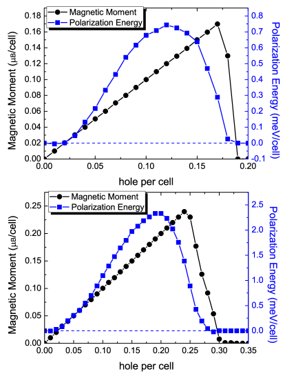
In the band-picture model, spontaneous ferromagnetism appears when the relative exchange interaction is larger than the loss in kinetic energy, that is, when it is satisfies the ”Stoner Criterion”: , where is the DOS at the Fermi energy and is the strength of the exchange interactionStoner1938 ; Peng2009 . As the DOS near VBE is rather large, we can dope hole into the system to increase . We check the stability of magnetization by calculating the polarization energy , which is defined as the difference between the nonspin-polarized and spin-polarized states. From Fig.4, we find that the ground state of the monolayer GaSe is ferromagnetic when the hole concentration is in the range from 0.02 to 0.18 per unit cell. While, the monolayer GaS becomes ferromagnetic in a wider range of hole concertration and the maximum hole concentration is 0.28 per unit cell from Fig 4. When the hole concentration is not in this range, is not large enough and the ”Stoner Criterion” is not satisfied, thus the system is nonmagnetic. The critical hole concentration for GaSe (0.18 hole per cell) corresponds to 1.24 cm-2. The low hole concentration in the system can be easily achieved by electric carrier doping, which has been used to induce superconductivity in MoS2Taniguchi2012 ; Ye2012 . The polarization energies in both cases first increase then decrease to zero with the increasing hole doping. The magnetic moment shows a linear relationship with hole concentration when the system is ferromagnetic. At optimal doping, polarization energies are 0.74 meV and 2.33 meV per cell for Ga2Se2 and Ga2S2, respectively. The corresponding magnetic moments are 0.12 and 0.20 per cell.
III The vacancy in Monolayer GaSe and GaS
According to Ref. Late2012, , the single-sheet GaS and GaSe show typitcal n-type and p-type conductance, respectively. These may be the consequence of intrinsic vacancies. The calculated formation energies of vacancies in both cases are shown in Table 1. In Se rich condition, the formation energy of a Ga vacancy is slightly less than that of a Se vacancy. Thus, a Ga vacancy is more favorable. This may explain the observed p-type conductance in GaSe. However, a Se vacancy is more favorable under Ga-rich condition. In GaS, the formation energies of a S vacancy are always negative under both conditions, indicating that S vacancies can be spontaneously introduced. Therefore, GaS is expected to be an intrinsic type, which is in agreement with experiment. The formation energy of a Ga vacancy in GaSe is less than that in GaS. In order to get magnetization, we need to dope hole into above systems, thus only Ga vacancies are discussed in the following.
denotes the two bonded Ga vacancy. GaSe GaS Environment Ga rich 2.97 5.72 1.53 4.29 7.35 -3.03 Se or S rich 1.81 3.40 2.69 2.93 4.64 -0.32
III.1 one Ga vacancy
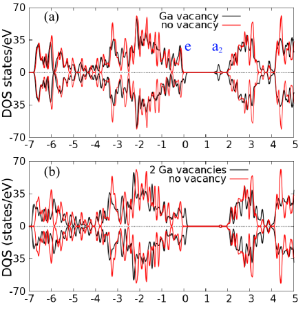
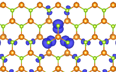
After relaxation, Se and S atoms surrounding the neutral Ga vacancy move outward while the Ga under the vacancy moves downward. Thus, the Se-Ga bond lengths in the top and the bottom layer shrink from 2.50 Åto 2.41 Åand 2.37 Åin monolayer GaSe, respectively. In monolayer GaS, the bond lengths of Ga-S in top and the bottom layer shrinks from 2.35 Åto 2.25 Åand 2.22 Å, respectively. Fig.5(a) shows the spin-resolved density of states (DOS) of the 44 supercell containing one Ga vacancy. A local moment of 1.0 is formed due to the spin polarization in both cases. The magnetic moments mainly locate at the three Se or S atoms surrounding the Ga vacancy, shown in Fig.6.
The formation of the local moment by Ga vacancy can be understood: The point group of monolayer GaX (X=Se, S) with a Ga vacancy is . A Ga vacancy leaves five unpaired electrons on the X and Ga atoms surrounding the vacancy. Under the influence of the crystal field, defect states associated with Ga vacancy are split into two singlet , and a doublet . The fully occupied state lies below the fermi level while is empty. Due to spin polarization, the state splits into spin-up and spin-down . Therefore, a Ga vacancy should result in a net local moment of 1 . The polarization energies are about 0.03 eV per defect site in GaSe and GaS.
III.2 Two Ga vacancies
With the vacancy of two bonded Ga , the mirror symmetry is restored in the system. The total magnetic moment, mainly localized at the Se atoms surrounding the vacancy, is 3.95 without relaxation. However, the magnetic moment vanishes after relaxation due to the movement of Se atoms surrounding the Ga vacancy. The length of Ga-Se bonds in both layers shrinks to 2.38 Å. The spin-resolved density of DOS of the 44 supercell containing two Ga vacancies shown in Fig.5(b). A local moment of 1.0 is formed due to the spin polarization in both cases.
Two Ga vacancies leave eight unpaired electrons on the surrounding Se atoms. Before relaxation, under the crystal field defect states are split into four singlets , , , and two doublets , . and are fully occupied while and are empty. The remaining four electrons occupied and due to large spin splitting. Thus, a net moment of 4 is formed. However, the energy of the states increases after relaxation. The energy of is higher than that . Therefore, the states are fully occupied, which results in a nonmagnetic state after relaxation.
IV The exchange coupling between vacancies
To investigate the magnetic coupling between these hole-induced magnetic moments, we employ the supercell with two vacancies in each subsupercell of . Two stable magnetic configurations (ferromagnetic and antiferromagnetic) can be obtained depending on the initial moments in the calculation. The Heisenberg type of spin coupling is: . Considering nearest-neighbor interactions, the magnetic energy of the FM state is: . For the case of AFM states, four nearest-neighbors have spins parallel and two have spins antiparallel. Thus, the magnetic energy is : . The energy difference of AFM and FM states is . Table 2 shows the energy difference and exchange coupling parameter for monolayer GaSe and GaS. In FM states, the total magnetic moment is always 2 for both cases. From Table 2, we find that FM states has a lower energy than the AFM states.
The observed FM state can be explained by kinetic exchange mechanismDev2008 . For the isolated Ga vacancy, the majority spin () is fully occupied, where the minority spin () is partially occupied. Therefore, the parallel spin alignment allows for the virtual hopping between the two defects states, which can lower the kinetic energy of the system. This hoping, however, is not allowed if the spin alignment is antiparallel.
We estimate the Curie temperature () based on the mean-field theory and Heisenberg model using the equation,
| (2) |
where is the onsite exchange parameter reflecting the exchange field created by all the neighboring magnetic moments. The estimated for monolayer GaSe and GaS are 50 and 26 K, respectively. The exchange coupling between local moment in GaSe is almost twice of that in GaS. It indicates the impurity state in GaS is more localized than that in GaSe.
| System | (meV) | J (meV) | (K) |
|---|---|---|---|
| 26.1 | 6.5 | 50 | |
| 13.4 | 3.4 | 26 |
V Conclusion
In summary, we perform DFT calculations to investigate the electronic structure of monolayer GaX. We find that monolayer GaSe(GaS) is a semiconductor with an indirect bandgap of 2.1(2.5) eV and there is a Van Hove singularity near the valence band edge. The monolayer GaX becomes ferromagnetic with small hole doping, which may be achieved by electric carrier doping in experiment. Under Se-rich condition, GaSe is intrinsic type induced by Ga vacancies. For GaS, a S vacancy can be spontaneously introduced, rendering GaS type. Ga vacancies can induce local moment around this defect. The coupling between the states of two Ga vacancies is ferromagnetic and extremely long-range.
VI Acknowledgments
We thank H. M. Weng for extremely useful discussion. The work is supported by ”973” program (Grant No. 2010CB922904 and No. 2012CV821400), the National Science Foundation of China (Grant No. NSFC-1190024, 11175248 and 11104339), and the Research Grant Council of Hong Kong SAR (Grant No. HKU706412P).
Note added–After this work is completed, we became aware of the paperCao2012 , which addresses the magnetism and half-metallicity in hole-doped monolayer GaSe.
References
- (1) K. S. Novoselov et al., Science 306, 666 (2004).
- (2) K. S. Novoselov et al., Nature (London) 438, 197 (2005).
- (3) Y. Zhang et al., Nature (London) 438, 201 (2005).
- (4) A. K. Geim and K. S. Novoselov, Nature Mater. 6 , 183 (2007).
- (5) K. K. Kim, Y. Shi, M. Hofmann, D. Nezich, J.?F. Rodriguez-Nieva, M. Dresselhaus, T. Palacios, and J. Kong, Nano Lett. 12, 161 (2012).
- (6) C. Tusche, H. L. Meyerheim, and J. Kirschner, Phys. Rev. Lett. 99, 026102 (2007).
- (7) D. Xiao, G.-B. Liu, W. Feng, X. Xu, and W. Yao, Phys. Rev. Lett. 108, 196802 (2012).
- (8) Q. H. Wang, K. Kalantar-Zadeh, A. Kis, J. N. Coleman and M. S. Strano, Nature Nanotech., 7, 699 (2012).
- (9) A. Splendiani, L. Sun, Y. Zhang, T. Li, J. Kim, C.-Y. Chim, G. Galli and F. Wang, Nano Lett., 10, 1271(2010).
- (10) K. F. Mak, C. Lee, J. Hone, J. Shan and T. F. Heinz, Phys. Rev. Lett., 105, 136805(2010).
- (11) X. Xu, W. Yao, D. Xiao and T. F. Heinz, Nature Phys., 10, 343(2014).
- (12) J. N. Coleman, M. Lotya, A. O Neill, S. D. Bergin, P. J. King, U. Khan, K. Young, A. Gaucher, S. De, R. J. Smith, I. V. Shvets, S. K. Arora, G. Stanton, H.-Y. Kim, K. Lee, G. T. Kim, G. S. Duesberg, T. Hallam, J. J. Boland, J. J. Wang, J. F. Donegan, J. C. Grunlan, G. Moriarty, A. Shmeliov, R. J. Nicholls, J. M. Perkins, E. M. Grieveson, K. Theuwissen, D. W. McComb, P. D. Nellist, and V. Nicolosi, Science 331, 568 (2011).
- (13) S. A. Wolf, D. D. Awschalom, R. A. Buhrman, J. M. Daughton, S. von Moln r, M. L. Roukes, A. Y. Chtchelkanova, and D. M. Treger, Science 294, 1448 (2001).
- (14) H. Ohno, Science 281, 951 (1998).
- (15) T. Dietl, H. Ohno, F. Matsukura, J. Cibert, and D. Ferrand, Science 287 , 1019 (2000).
- (16) T. Jungwirth, J. Sinova, J. Masek , J. Kucera, and A. H. MacDonald, Rev. Mod. Phys. 78, 809 (2006).
- (17) R. Monnier and B. Delley, Phys. Rev. Lett. 87, 157204 (2001)
- (18) I. S. Elfimov, S. Yunoki, and G. A. Sawatzky, Phys. Rev. Lett. 89, 216403 (2002).
- (19) M. Venkatesan, C. B. Fitzgerald, and J. M. D. Coey, Nature (London) 430, 630 (2004).
- (20) H. Pan, J. B. Yi, L. Shen, R. Q. Wu, J. H. Yang, J. Y. Lin, Y. P. Feng, J. Ding L. H. Van, and J. H. Yin, Phys. Rev. Lett. 99, 127201 (2007).
- (21) P. Dev, Y. Xue and P. H. Zhang, Phys. Rev. Lett. 100, 117204 (2008).
- (22) H. W. Peng, H. J. Xiang, S. H. Wei, S. S. Li J. B. Xia and J. B. Li, Phys. Rev. Lett. 102, 017201 (2009).
- (23) K. Kusakabe and M. Maruyama, Phys. Rev. B 67, 092406 (2003).
- (24) Y.-H. Kim, J. Choi, K. J. Chang, and D. Tomanek, Phys. Rev. B 68, 125420 (2003).
- (25) J. A. Chan et al., Phys. Rev. B 70, 041403 (2004).
- (26) A. N. Andriotis, R. M. Sheetz, E. Richter, and M. Menon Europhys. Lett.72, 658 (2005).
- (27) R. F. Liu and C. Cheng, Phys. Rev. B 76, 014405 (2007).
- (28) O. V. Yazyev and L. Helm, Phys. Rev. B 75, 125408 (2007).
- (29) Y. Zhang, S. Talapatra, S. Kar, R. Vajtai, S. K. Nayak, and P. M. Ajayan, Phys. Rev. Lett. 99, 107201 (2007).
- (30) Y. G. Zhou, P. Yang, H. Y. Zu, F. Gao and X. T. Zu, Phys. Chem. Chem. Phys., 15, 10385 (2013).
- (31) A. Segura, J. Bouvier, M.V. Andres, F. J. Manjon, and V. Munoz. Phys. Rev. B, 56, 4075 (1997).
- (32) S. Nusse, P.H. Bolivar, H. Kurz, V. Klimov and F. Levy, Phys. Rev. B, 56, 4578 (1997).
- (33) K. Kato, N. Umemura, Optics Letters, 36, 746 (2011).
- (34) P.A. Hu, Z.Z. Wen, L.F. Wang, P.H. Tan, K. Xiao, ACS Nano, 6, 5988 (2012).
- (35) D. J. Late, B. Liu, J.J. Luo, A.M. Yan, H.S.S.R. Matte, M. Grayson, C.N.R. Rao, V.P. Dravid, Advanced Materials, 24 3549 (2012).
- (36) V. Zolyomi, N. D. Drummond and V. I. Falko, Phys. Rev. B 87, 195403.
- (37) G. Kresse and J. Hafner, Phys. Rev. B 47, 558 (1993).
- (38) G. Kresse and J. Furthmuller, Comput. Mater. Sci. 6, 15 (1996).
- (39) G. Kresse and J. Furthmuller, Phys. Rev. B 54, 11169 (1996).
- (40) J. P. Perdew, K. Burke, and M. Ernzerhof, Phys. Rev. Lett. 77, 3865 (1996).
- (41) E. C. Stoner, Proc. R. Soc. A 165, 372 (1938); 169, 339 (1939).
- (42) K. Taniguchi, A. Matsumoto, H. Shimotani and H. Takagi, Appl. Phys. Lett. 101, 042603 (2012).
- (43) J. T. Ye, Y. J. Zhang, R. Akashi, M. S. Bahramy, R. Arita and Y. Iwasa, Science 338, 1193(2012).
- (44) T. Cao, Z. L. Li, S. G. Louie,arxiv:1409.4112.