Investigation of defect cavities formed in three-dimensional woodpile photonic crystals
Abstract
We report the optimisation of optical properties of single defects in three-dimensional (3D) face-centred-cubic (FCC) woodpile photonic crystal (PC) cavities by using plane-wave expansion (PWE) and finite-difference time-domain (FDTD) methods. By optimising the dimensions of a 3D woodpile PC, wide photonic band gaps (PBG) are created. Optical cavities with resonances in the bandgap arise when point defects are introduced in the crystal. Three types of single defects are investigated in high refractive index contrast (Gallium Phosphide-Air) woodpile structures and Q-factors and mode volumes () of the resonant cavity modes are calculated. We show that, by introducing an air buffer around a single defect, smaller mode volumes can be obtained. We demonstrate high Q-factors up to 700000 and cavity volumes down to . The estimates of and are then used to quantify the enhancement of spontaneous emission and the possibility of achieving strong coupling with nitrogen-vacancy (NV) colour centres in diamond.
pacs:
(160.5298) Photonic crystals; (140.3945) Microcavities; (270.5580) Quantum electrodynamics; (350.4238) Nanophotonics and photonic crystals.I Introduction
In recent years, there has been remarkable progress in designing and fabricating three-dimensional (3D) photonic crystal based optical micro-cavities containing suitable emittersHo2011:IEEE_JQE ; Tandaechanurat2010 ; Aoki2003 ; Ishizaki2009 ; Qi2004 ; Lin2005 ; Braun2006 ; Ozbay1994 . Such systems show long photon life times (i.e. high Q-factors) and small mode volumes (). The resulting strength of interaction between the cavity photons and a two-level system leads to dramatic modifications of spontaneous emission Purcell1946 ; Benisty1998a ; Hennessy2007 ; Lodahl2004 and cavity quantum electro dynamical (cavity-QED) phenomena Thompson1992 ; Reithmaier2004a ; Peter2005a ; Hennessy2007 ; Englund2007 known generically as strong coupling. Potential applications of these devices include electro-optic modulators Tanabe2009 ; Zhang2013 , photonic sensors Chakravarty2014 ; Zhang2014 , ultra-small optical filters Song2003 , nonlinear optical devices Corcoran2009 , ultralow-power and ultrafast optical switches Nozaki2010 , quantum information processing Xiao2008 ; Young2009 ; Young2011 ; Hu2011 and low threshold lasersLoncar2002 . Some of these achievements have been reported using two-dimensional (2D) PC slab cavities Fujita2005 and waveguides Schwagmann2011 , which are easier to fabricate and simulate. However, in 2D PC designs, it is difficult to design low volume high finesse cavities due to the out-of plane radiation losses and scattering. In contrast, 3D PC designs provide stronger confinement due to their complete photonic band gap Yablonovitch1987 ; Ho1990 leading to smaller mode volumes thus larger effects with weaker emitters.
Recently, several 3D PC structures with complete PBGs have been simulated and fabricated using two-photon polymerization (2PP) based 3D lithography or direct laser writing (DLW) system, with or without backfilling materials to create 3D high-refractive-index-contrast nanostructures Deubel2004:nanoscribe ; VonFreymann2010 ; website:nanoscribe . In this work, we investigate the potential to create high-Q low mode volume cavities using the optical properties of single defects in three-dimensional (3D) face-centred-cubic woodpileHo1994:OriginalWoodpile photonic crystal cavities. Analysis using the plane-wave-expansion (PWE) method has shown a full photonic bandgap in technically interesting wavelength regions. We have studied the optimisation of relative gap width (gap width to midgap frequency ratio) as a function of the rod width using MIT Photonic-Bands software (MPB) Johnson2001:mpb ; website:MPB . Our in-house finite-difference time-domain software Railton:BristolFDTD is then used to calculate the time response and transmission spectrum of the finite woodpile crystal structures containing three types of single defect cavities with and without an air buffer to further isolate the cavity. We demonstrate high Q-factors up to 700000 - limited only by simulation volume constraints - and cavity volumes down to . Our Q-factors are comparable to other reported structures McCutcheon2008 ; Vahala2003 ; vahala-ref-48 ; vahala-ref-62 , but we note that it is the much smaller cavity volumes, which are of interest here. These cavity volumes are an order of magnitude smaller than recent woodpile cavity simulations Woldering2014 and a factor of four smaller than nanobeam cavities McCutcheon2008 . By introducing an air buffer around the defect, even smaller mode volumes can be obtained with slightly lower Q-factors. We then estimate the enhancement of spontaneous emission and possibility of achieving strong coupling. As an example system, we use emission rates estimated from nitrogen-vacancy (NV) colour centres in nanodiamond embedded in 3D FCC woodpile PhC structures made of gallium phosphide.
II Geometry and bandgaps: 3D FCC woodpile photonic crystal cavity design
II.1 Geometry: Design of the model
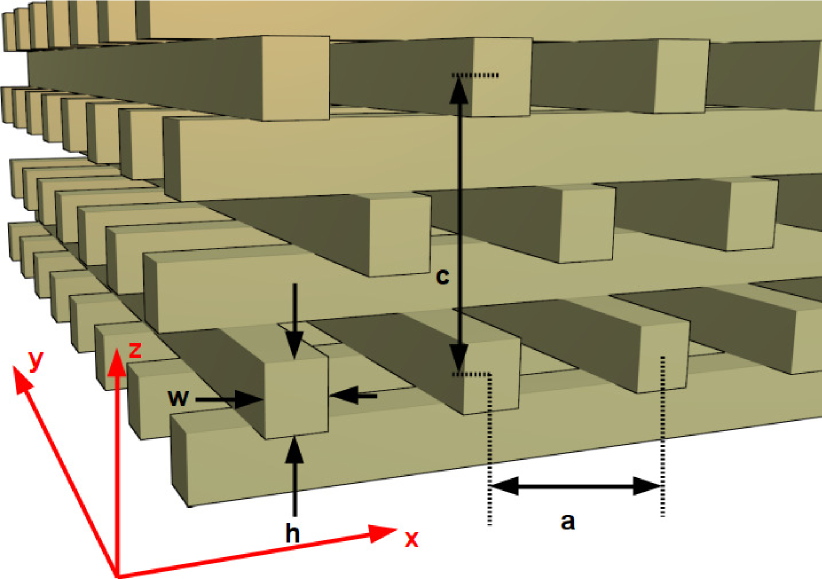
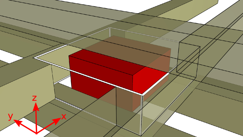
We are studying the woodpile structure as shown in figure 1(a). A woodpile structure consists of layers of parallel dielectric rods, with each layer rotated by 90° relative to the other. Additionally, the layers are shifted by half a period every 2 layers. This means that the structure repeats itself in the stacking direction every 4 layers. We define the period along the stacking direction, corresponding to 4 layers, as and the distance between two rods within each layer as . In our case, the rods have a rectangular cross-section with a height and width . For a non-infinite woodpile crystal, we also define the number of layers and the number of rods per layer . In our simulations, to make the woodpile more symmetric, the number of rods per layer actually varies from to .
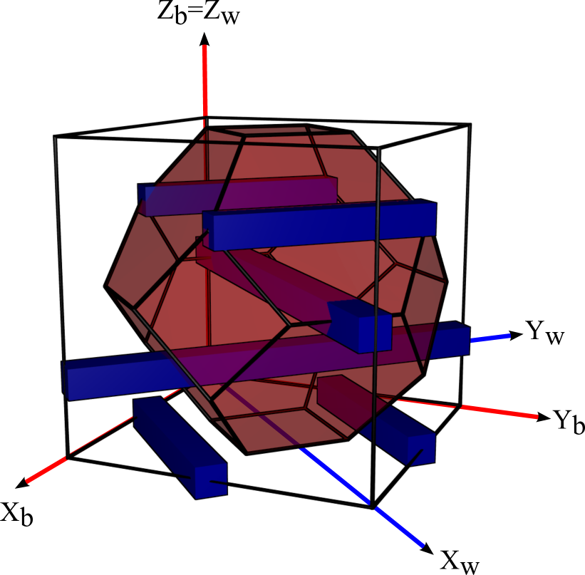
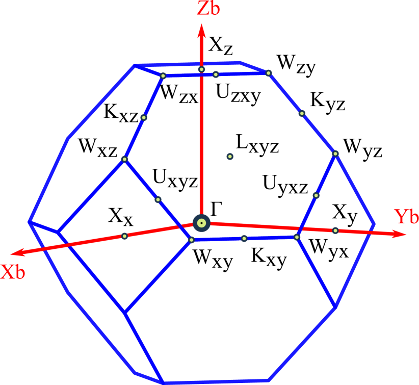
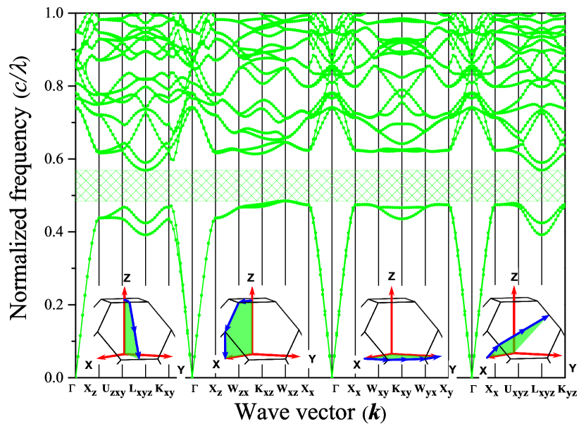
Depending on the ratio , the woodpile corresponds to different crystal lattices. For , it corresponds to a body-centered-cubic (BCC) lattice, for , to a face-centered-cubic (FCC) lattice and otherwise to a centered-tetragonal lattice. Here we chose , i.e. an FCC lattice as this has the most ’spherical’ Brilluoin zone and thus produces the widest bandgaps. Figure 2(a) illustrates the Brillouin zone of the FCC lattice relative to the woodpile. While the FCC woodpile shares the translational symmetry of an FCC lattice, it does not have the same rotational symmetries. The usual “X points” of the FCC brillouin zone are no longer equivalent. We therefore used more specific labels for the FCC brillouin zone as detailed in figure 2(b). We orient the brillouin zone in the basis and the woodpile in the basis with , , . The layers in our woodpiles are stacked along the direction and the rods aligned along the and directions.
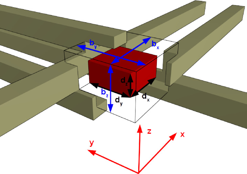
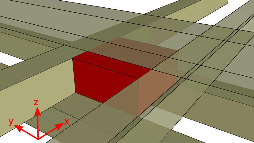
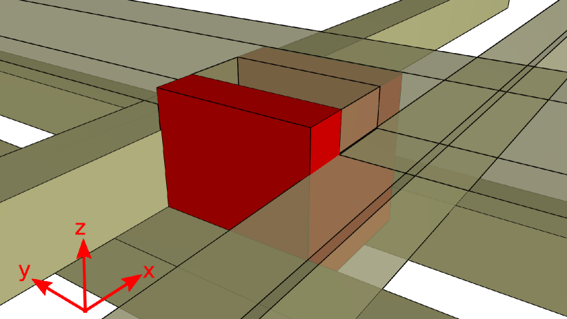
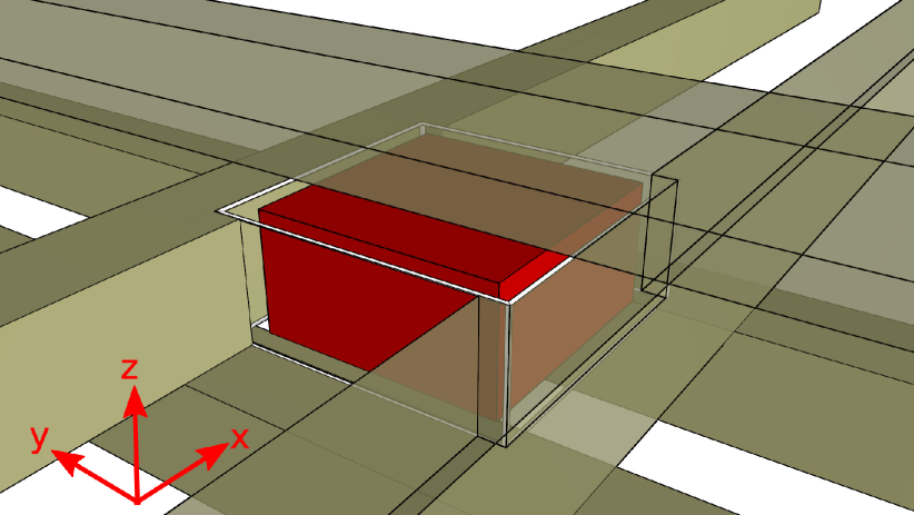
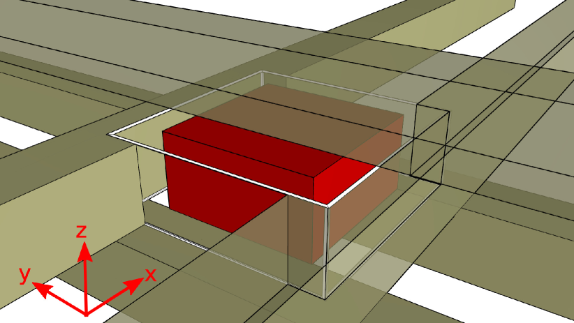
In order to create a resonant cavity in which the photons will be confined, a defect has to be added to the crystal Ho2011:IEEE_JQE ; Ishizaki2013 ; Woldering2014 . Following our previous work Ho2011:IEEE_JQE , adding sphere based defects to air sphere crystals, here we choose a cuboid defect. The defect position is shown in figure 1(b). It is centered between two rods of the middle layer (with rods along the axis) and positioned along so that it is situated under a rod from the layer directly above it.
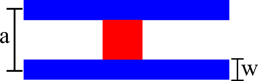
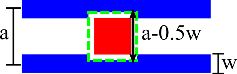
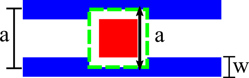
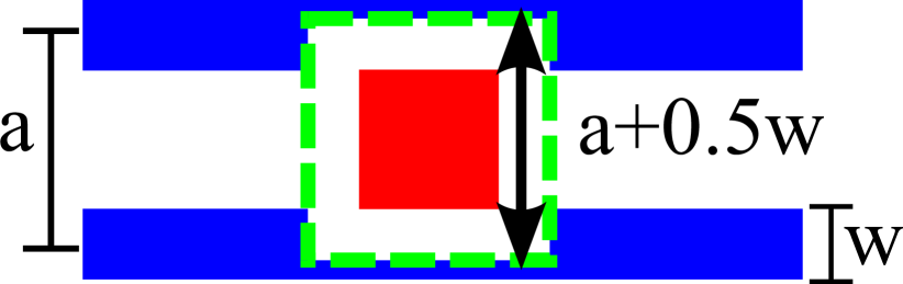
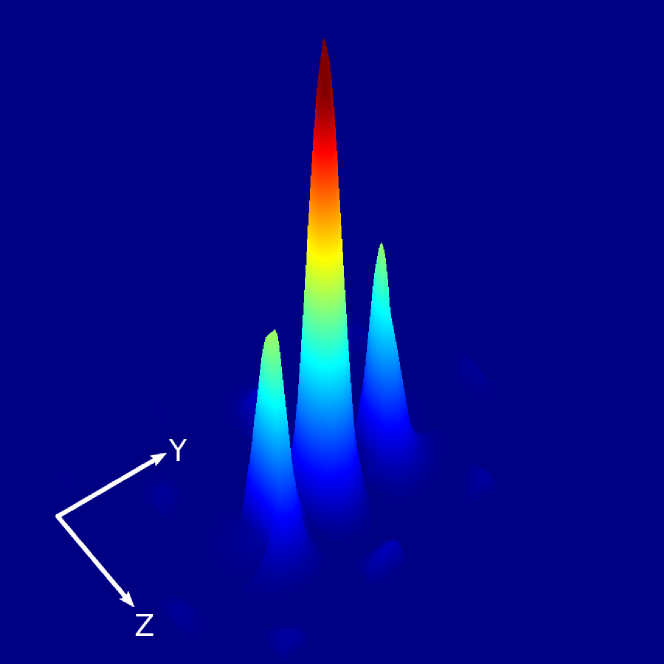
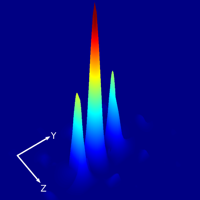
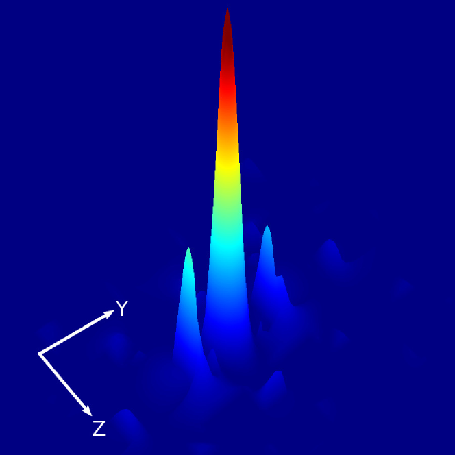
We initially conducted simulations for a fixed defect size, but at different positions within the woodpile. First, so that it is not directly over/under a rod from the adjacent layer, second with the defect placed on a rod. We found that the confinement properties were worse (lower Q-factor, larger mode volume) than for the position between the rods (described above and in figure 1(b)) thus we chose this symmetry for all the work reported here. However, we consider three different defect sizes D0, D1 and D2, as illustrated in figures 3(a), 3(b) and 3(c). In an attempt to reduce the energy leakage from the defect into the woodpile, we also looked at the effect of adding a cuboid air buffer around the defect D1 (i.e. in the same position, but larger than the defect). Three different air buffer sizes A0, A1 and A2, as illustrated in figures 4(a), 4(b) and 4(c) were considered. For our simulations, we used and an experimentally relevant refractive index (corresponding to Gallium-Phosphide (GaP), for example) for the woodpile rods and the defect. The air buffer and the backfill material is considered to be air/vacuum of refractive index . For the non-infinite woodpile crystal, we used and .
II.2 Bandgaps: Photonic bands of a 3D FCC woodpile PhC without defects
Initially, it is necessary to find the allowed propagation modes and eventual bandgaps of our photonic crystal. To do this, we used the MIT photonic bands package, which solves the frequency domain eigenproblem for a periodic dielectric structure Johnson2001:mpb ; website:MPB , giving us the allowed propagation modes for different wavevectors . The results for the woodpile structure described above using are shown in figure 5(a). A full bandgap from to is clearly seen.
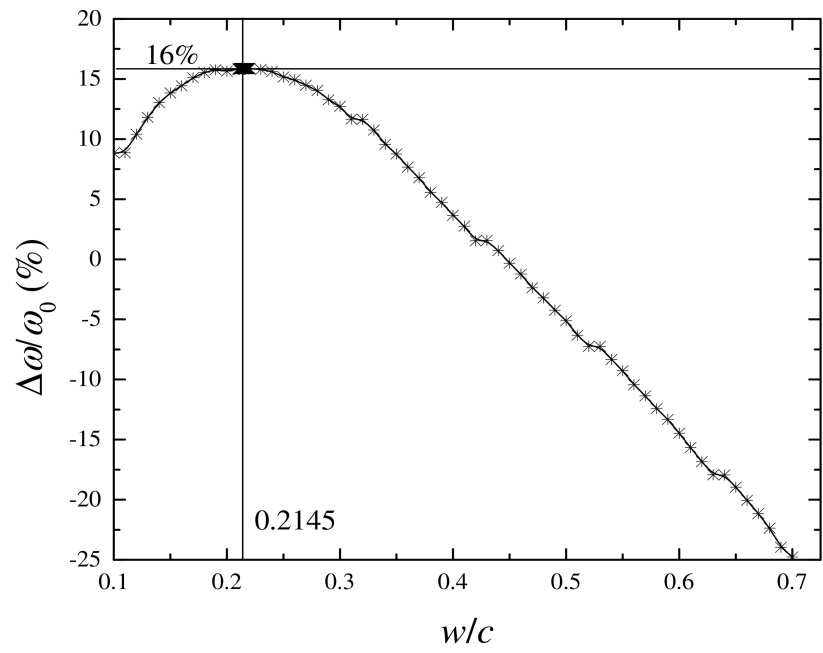
This value of was chosen after calculating the gap-midgap ratio as a function of . Figure 5(b) shows the results of these calculations, with a maximum gap-midgap ratio of for .
III Calculating relevant parameters of the D1 cavity
In the following, we show how we calculate relevant parameters for our cavity structures. These are the cavity resonant wavelength , the quality factor , the mode volume , the Purcell factor and the coupling strength . We use as detailed example the D1 cavity described earlier in figure 3(b).
III.1 Resonant wavelength and Q-factors of cuboid defect cavities with and without air buffers
Now that the frequency range of the full photonic bandgap has been ascertained, we will look at the confinement efficiency of different defect cavities within this woodpile. To do this we use a finite woodpile with a defect, as previously described in section II.1. We then add a broadband source covering the bandgap within the defect and look at the time decay of the electromagnetic field using FDTD. In order to better distinguish modes, we simulate using three orthogonal orientations of the dipole in 3D space: along the , and axis, which we designate by , and respectively.
The centre of the bandgap is at . For , which corresponds to the zero-phonon line (ZPL) of nitrogen-vacancy centres (NV centres) in diamond, the corresponding vertical period of the woodpile is . The other parameters are then for the horizontal period inside each layer, for the rod width and for the rod height.
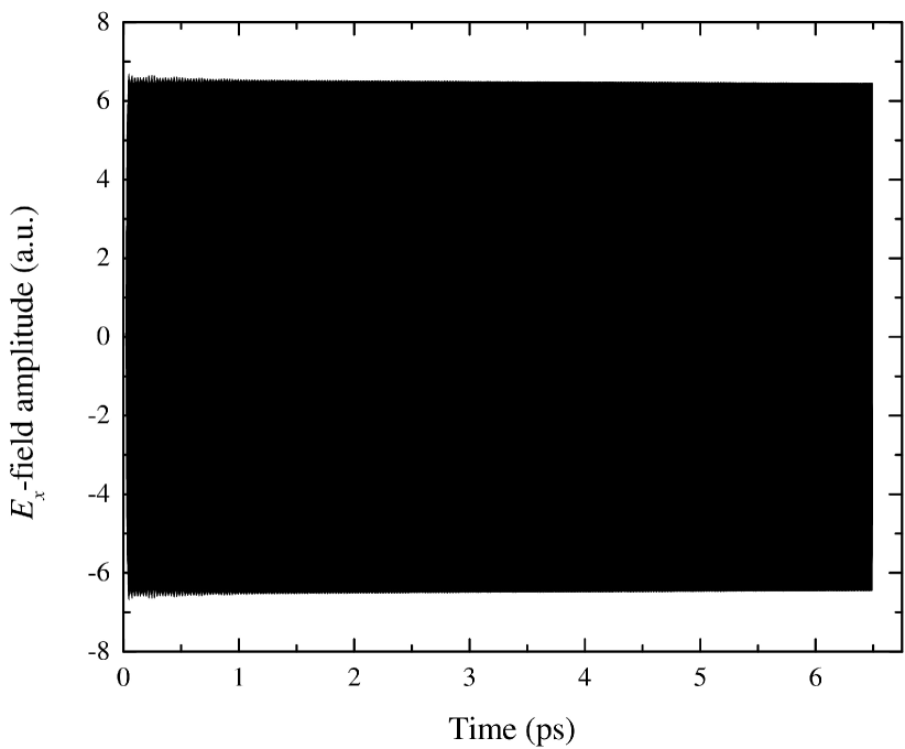
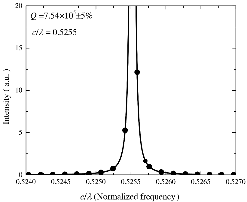
In the simulation a field probe is placed close to the excitation dipole located , or away from it depending on its direction. The field at this probe is monitored as the simulation progresses and we obtain a slowly decaying field amplitude oscillating primarily at the allowed frequencies of the cavity. Hence taking the fast Fourier transform (FFT) of this ringdown signal allows us to determine the resonant frequencies of the cavities and gives us an estimate of the Q-factors of these resonances ().
As these are high-Q (long time decay) resonances, the FDTD simulations were run for iterations (timestep , total time ) in order to confirm the field decayed significantly by the end of the simulation. A single simulation using a non-homogeneous mesh of around cells adapted to the geometry takes about 2 weeks on a computing node with two 2.8 GHz quad-core Intel Harpertown E5462 processors, using a single core (as unfortunately, our software does not support parallel processing) and 2 out of the available 8GB of RAM memorywebsite:ACRC . The field decay and spectrum for a woodpile with defect D1 is shown in figure 6 illustrating the simple method of calculating Q. In many structures, we do not achieve a full decay of the field: this limits the Q values measured from the FFT peaks. Hence, for the analysis of very long lived decays corresponding to very narrow spectral features, we also analyze the ringdown signal using the filter diagonalization method Mandelshtam1997:harminv via the Harminv software website:harminv , which extracts the decay rates and frequencies of the high-Q cavity modes.
III.2 Calculating the effective mode volume
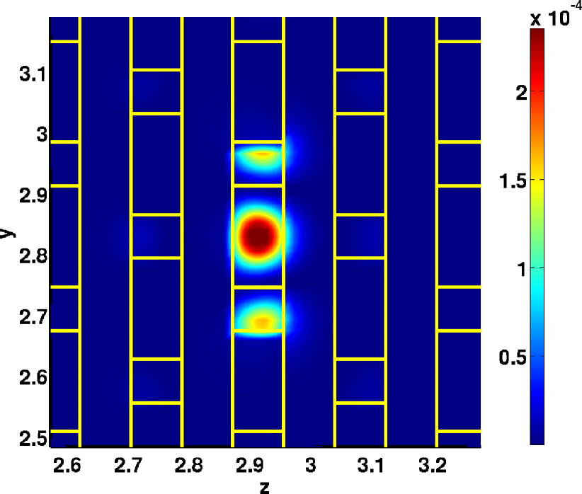
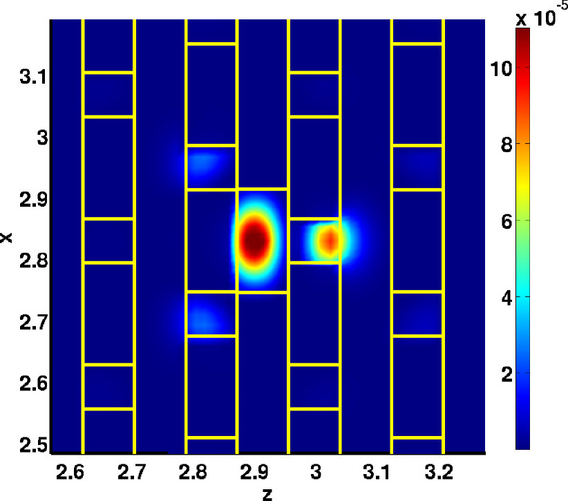
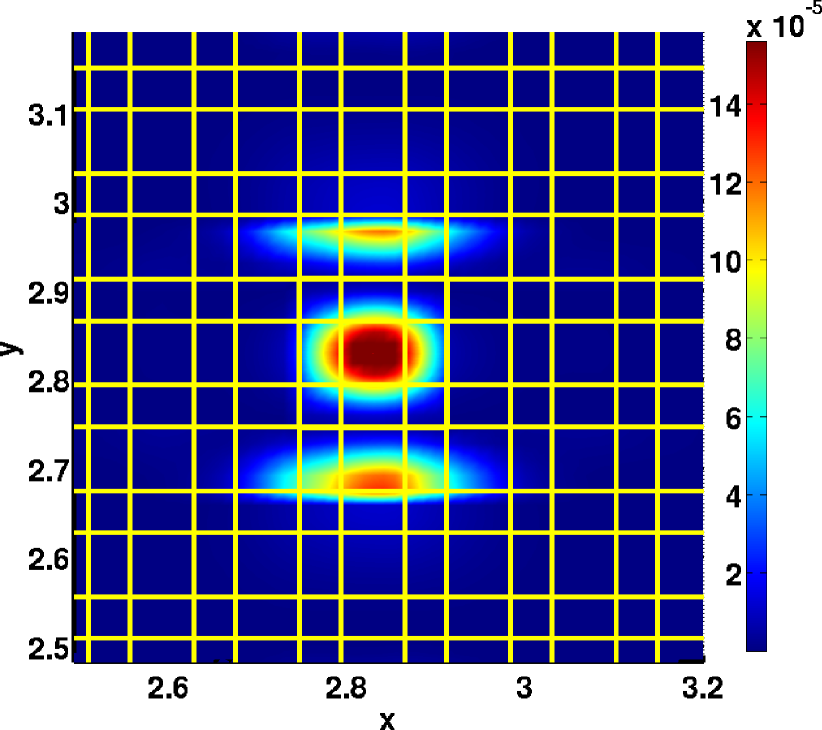
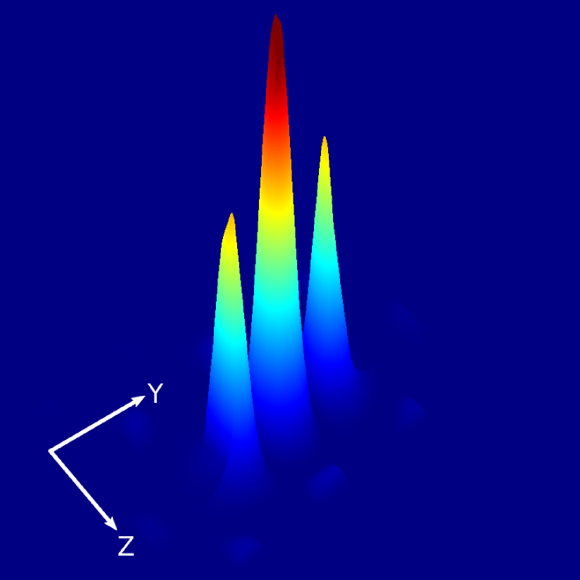
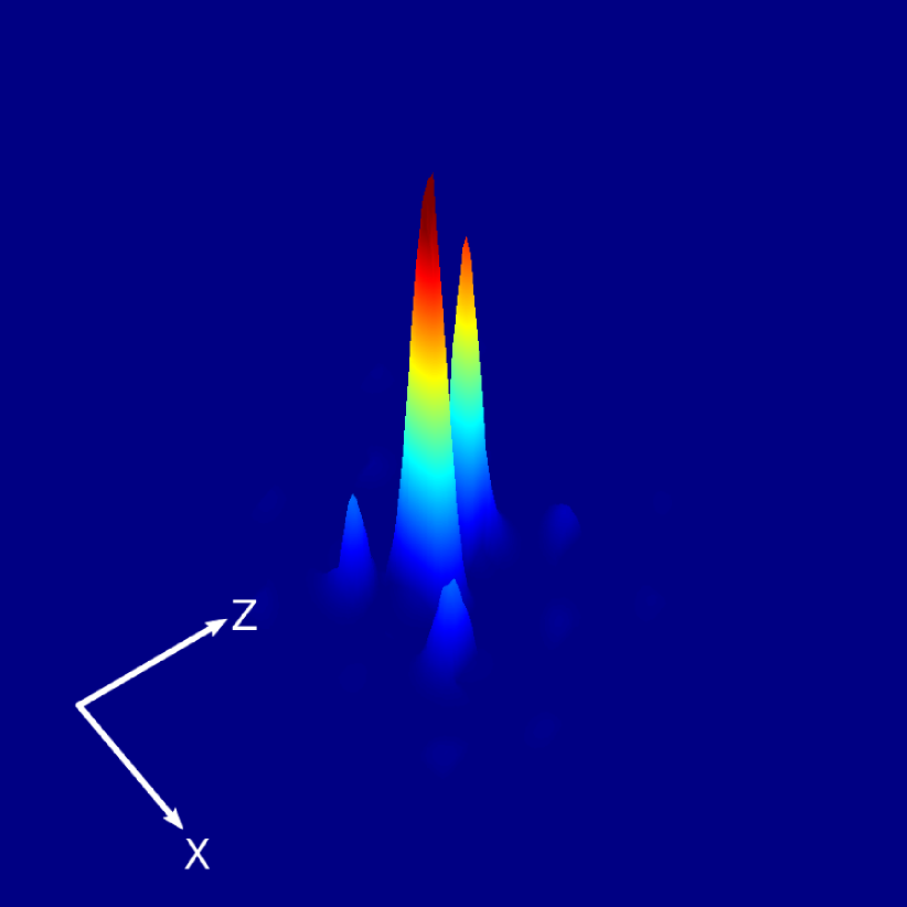
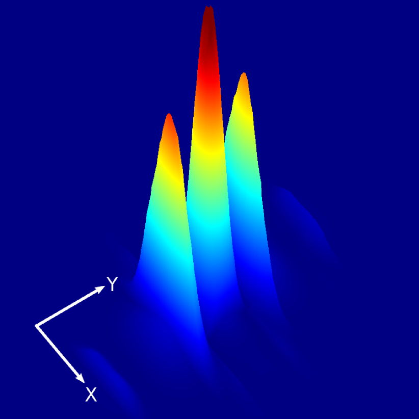
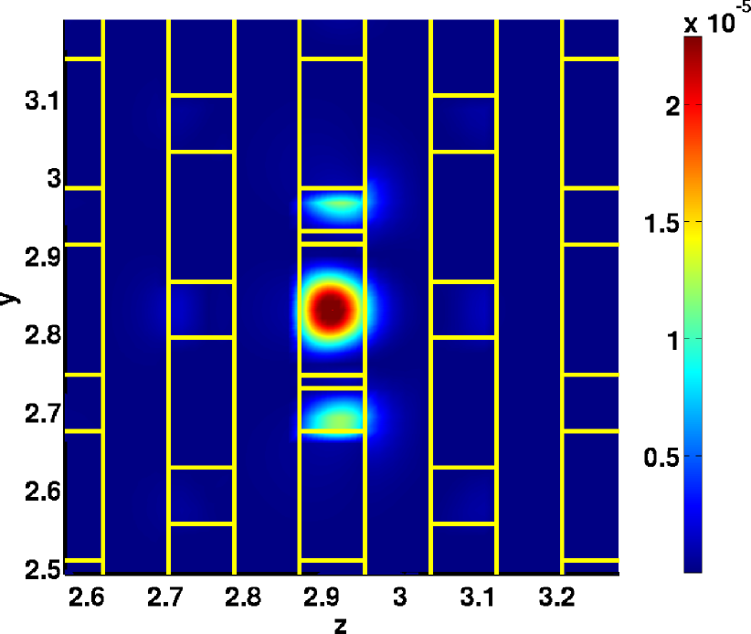
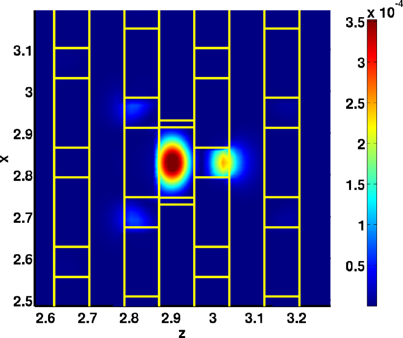
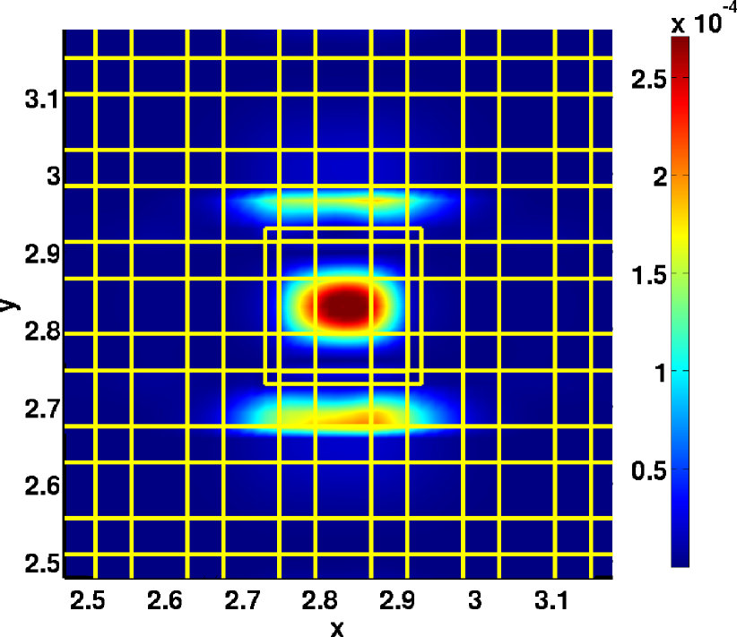
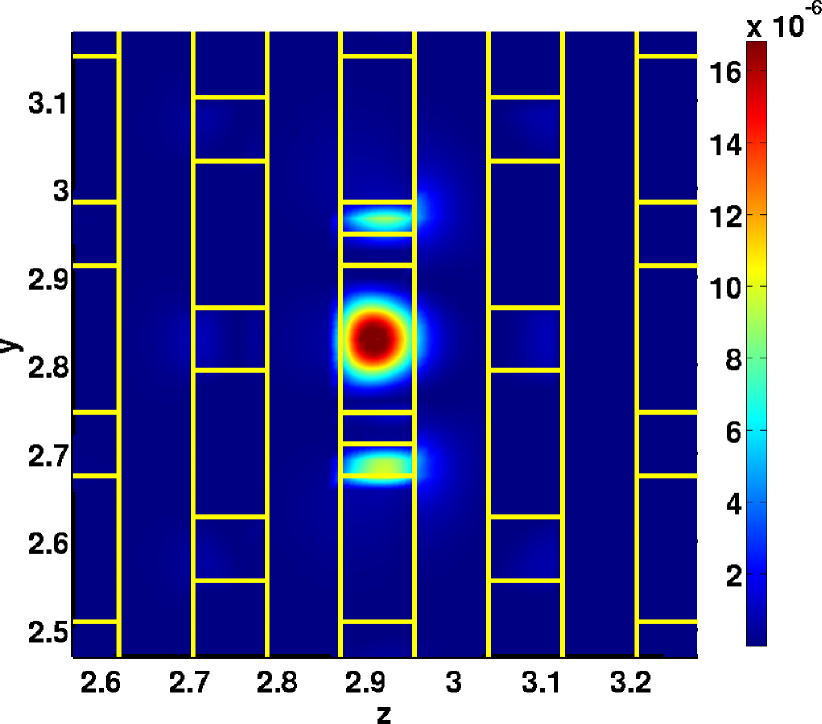
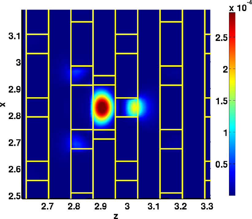
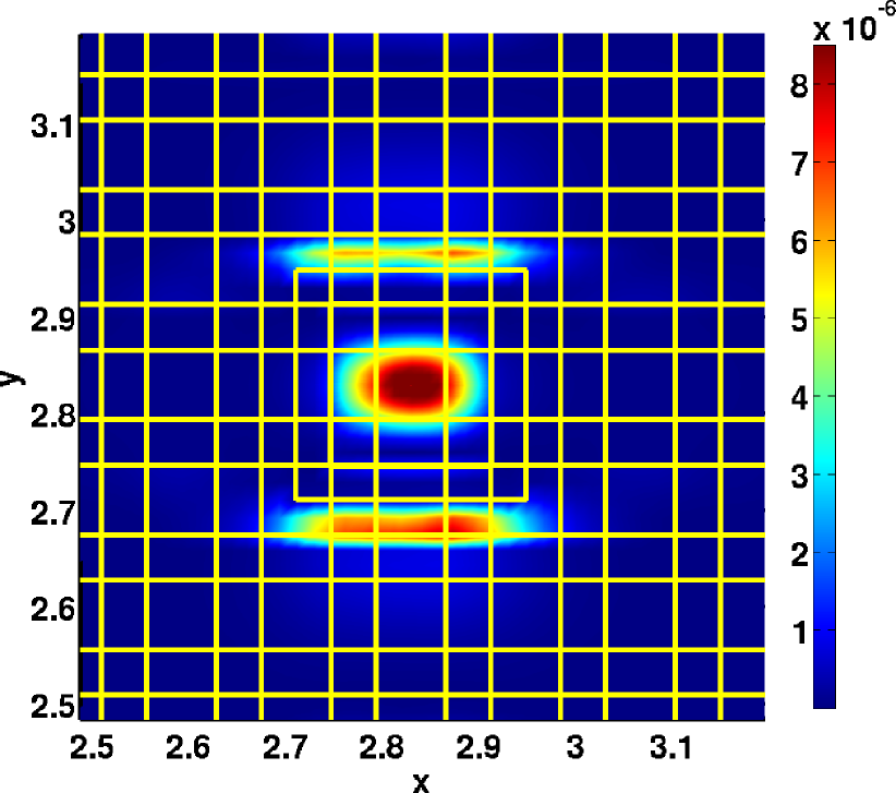
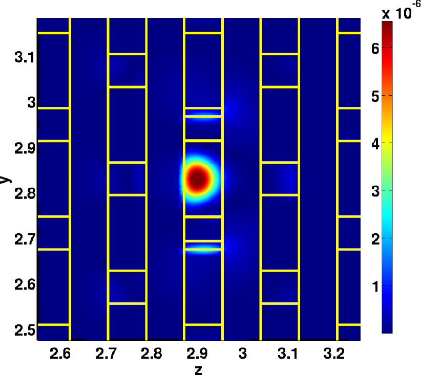
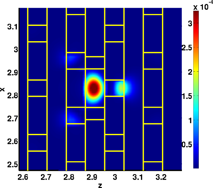
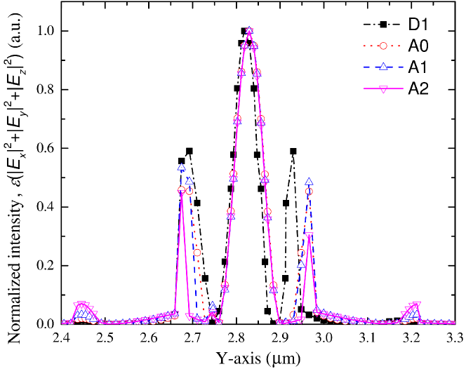
Having determined the resonant frequency, we can visualise a cavity mode on resonance using single frequency ”snapshots”. We illustrate the confinement of the electric field energy density distribution in each plane y-z, x-z, and y-x in figure 7 for the defect D1. It shows x, y, and z projections of the woodpile superimposed over the electric field energy density distributions (, although the plotted values are actually with ) of a defect for an oriented dipole mode.
In all cases the field is strongly localised to the defect, with some spread to the high refractive index links nearby. The FDTD algorithm allows a computation of the effective mode volume of the cavity modes with high Q-factor, which is the 3D PhC cavity mode that survives after a sufficiently long period of time. We do this by creating a sequence of resonant frequency ”snapshots” through the resonant mode, covering all grid points, then digitally summing the fields using the definition of the effective mode volume :
| (1) |
We see that is given by the spatial integral of the electric field intensity for the cavity mode, divided by its maximum value. The in (1) is equal to and therefore proportional to the square of the spatially dependent refractive index . A figure of merit is the dimensionless effective volume , which is the effective cavity mode volume normalised to the cubic wavelength of the resonant mode in a medium of refractive index , defined as:
| (2) |
Since is proportional to the inverse square root of the mode volume (), the field coupling strength can be enhanced by reducing .
III.3 Estimating the Purcell enhancement and the coupling strength
In order to evaluate the usefulness of the simulated cavities for quantum information applications, we estimate how strongly a quantum emitter, which can be considered as a transition dipole, placed inside it will interact with the vacuum field created by the cavities. A strong interaction means it will be possible to entangle photon states with quantum emitter states.
In this paper, we consider diamond NV-centres as an example quantum emitter. Diamond NV-centres are interesting due to their stability as a single photon source, their long spin decoherence time () and their ability to generate indistinguishable photons at low-temperatures Sipahigil2012 ; Bernien2012 . Additionally, their availability in the form of defects in nanocrystals makes it possible to embed them within photonic crystals fabricated using a different material, for instance 3D photonic crystals made via direct laser writing.
III.3.1 Emission spectrum and coupling rate of a coupled dipole-cavity system:
When the cavity mode radial frequency is equal to the transition dipole radial frequency (corresponding to the energy difference between the ground and excited state of the quantum emitter) and if the dipole has the same polarization as the cavity mode, the luminescence spectrum for such a system isCarmichael1989 ; Andreani1999 :
| (3) |
where and:
| (4) |
is the full width at half-maximum (FWHM) of the cavity mode, corresponding to the rate of escape of photons from the cavity, and is the FWHM of the emission spectrum of the quantum emitter dipole without any cavity (equivalent to its spontaneous emission rate assuming no other broadening processes). For diamond NV-centres, we take the emission rate into the zero-phonon line which is resonant with the cavity: Ho2011:IEEE_JQE ; McCutcheon2008 ; Wolters2010a ; Santori2010a ; Collins1983 ; Beveratos2002 .
The dipole-cavity coupling rate is given byAndreani1999 :
| (5) |
and are the elementary charge and mass of an electron respectively, is the vacuum permittivity, is the refractive index of the defect, where the dipole is located and is the mode volume of the cavity mode. is the oscillator strength of the dipole given by:
| (6) |
where is the dipole moment of the quantum emitter:
| (7) |
is the refractive index of the material directly surrounding the quantum emitter. In the case of NV-centres, this is diamond with .
| (8) |
III.3.2 Strong/weak coupling limit:
As illustrated in Khitrova2006 , the luminescence spectrum given in (3) corresponds to a superposition of two peaks, with central frequencies and and whose linewidths are:
| (9) | |||||
| (10) | |||||
| (11) | |||||
| (12) |
When , the general two peak spectrum collapses to a single peak at frequency . This is called the weak coupling regime. When , there are two separate frequency components at and this is called the strong coupling regime. However, this only leads to two separate peaks in the spectrum for:
| (13) |
This is the commonly used condition for strong coupling. The weak and strong coupling regimes are characterised by the reversibility of the emission. In the weak coupling regime, photons emitted by the quantum emitter are very unlikely to be reabsorbed by it, i.e. the emission is irreversible. The converse is true for the strong coupling regime where emitted photons are very likely to be reabsorbed by the quantum emitter, i.e. the emission is reversible.
III.3.3 Spontaneous emission modification: Purcell factor:
In the weak coupling regime, for varying values of , tends to stay close to , while stays close to . therefore corresponds to the emission rate of the coupled dipole, while corresponds to the decay rate of the coupled cavity mode. The modification of the spontaneous emission rate can thus be quantified by the so-called Purcell factor:
| (14) |
III.3.4 Purcell factor approximation in the weak coupling regime:
In the weak coupling regime, when , but also when (which is usually the case) and , and can be simplified toAndreani1999 :
| (15) | |||||
| (16) |
| (17) |
When the nano-diamond is small () and embedded in a defect, . This allows us to further simplify (17) to the well known approximation of the Purcell factor in the weak coupling regime:
| (18) |
This is the approximation we used for the values presented in tables table 1 and table 2 and figure 8(c). However, due to the strong coupling we obtained in most cases, it is not a valid indicator of the spontaneous emission modification. In the strong coupling region the peak splitting leads to an oscillating probability of emission which decays at a rate largely determined by the cavity lifetime.
IV Results
IV.1 Results for different defect sizes
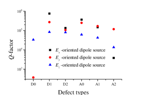
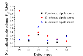
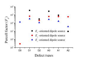
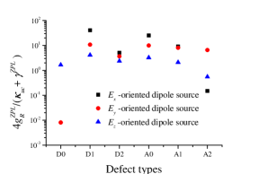
First, we look at the defects without air buffers D0, D1 and D2. Table 1 and figure 8 show the corresponding results. Simulations for the defect D0 in the direction showed no clearly distinguishable resonance modes, which is why its entries in table 1 are marked n/a. The defect D1 gives the best results for an excitation in the direction with a Q-factor and a mode volume .
In terms of coupling strength, all defects without air buffer exhibit strong coupling capabilities, except D0 in the and directions. Even in the direction, it barely exceeds the strong coupling condition with and . It does however offer a spontaneous emission enhancement of .
D1 shows the best coupling strength with and . For both D1 and D2, when moving from excitations to and excitations, the Q-factors become smaller and the mode volumes larger, i.e. the confinement properties get worse. We think this is because dipoles in the and directions emit most of their energy in the XZ and XY plane respectively, but since the emitter is placed between two rods in the X direction, there is nothing preventing energy escaping along the X direction, apart from the defect box itself.
IV.2 Results for different air buffer sizes
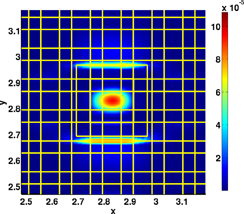
We now concentrate on the defect D1, which gave the best results. As can be seen on the corresponding energy snapshots in figure 7, the energy tends to leak into the rods touching the defect. In order to improve the confinement, i.e. reduce the leakage, we therefore now add the previously mentioned cuboid air buffers around the defect to disconnect it from the surrounding rods. Table 2 and figures 9 and 8 show the results for the defects with air buffers A0, A1 and A2. This essentially corresponds to ”cutting” into the rods by , and . Since and there is a rod touching the top of the defect as can be seen in figures 4(a), 4(b), 4(c), the structure remains contiguous and could be fabricated directly or as an inverse for backfilling with high refractive index material.
Figures 10 and 11 show that the two peaks on the side of the main energy peak in the YZ plane are indeed reduced by the air buffers, the most efficient being the air buffer used in A2. However, while the mode volume also dropped as expected for the excitation in the A0 and A1 defects, it instead increased for the A2 defect. A2 is also the only one of the defects with air buffers not suitable for strong coupling, with for an excitation and for an excitation. The corresponding emission enhancements are and .


| Defect type | D0 | D1 | D2 | ||||||
|---|---|---|---|---|---|---|---|---|---|
| Defect size | |||||||||
| Air buffer size | |||||||||
| Dipole orientation | |||||||||
| (GHz) | |||||||||
| (ns) | |||||||||
| Diamond NV centres | Diamond nanocrystals: | ||||||||
| (GHz) | |||||||||
| (ns) | |||||||||
| (GHz) | () | ||||||||
| (V/m) | |||||||||
| (GHz) | |||||||||
| (ns) | |||||||||
| Defect type | A0 | A1 | A2 | ||||||
|---|---|---|---|---|---|---|---|---|---|
| Defect size | |||||||||
| Air buffer size | |||||||||
| Dipole orientation | |||||||||
| (nm) | |||||||||
| (GHz) | |||||||||
| (ns) | |||||||||
| Diamond NV centres | Diamond nanocrystals: | ||||||||
| (GHz) | |||||||||
| (ns) | |||||||||
| (GHz) | () | ||||||||
| (V/m) | |||||||||
| (GHz) | |||||||||
| (ns) | |||||||||
The smallest mode volume and biggest coupling strength are obtained for the defect A0 (figure 4(a)), with and . The corresponding Q-factor is lower than for the same defect without air buffer where , which leads to a weaker coupling with . But since the Q-factor can be increased by increasing the number of periods of the woodpile structure, Ho2011:IEEE_JQE ; Imagawa2012 ; Tajiri2014 , stronger coupling could still be achieved, still rendering this kind of air buffer useful.
V Conclusion
In this article, we have investigated 3D FCC woodpile photonic crystals formed in high-index-contrast materials (GaP) and found a maximum photonic band gap (PBG) of at by using the plane-wave expansion method. We also introduced cuboid-shaped defects with various sizes near the centre of the middle layer in the 3D PhCs and calculated the Q-factors and mode volumes of cavity modes using the FDTD method. The best results were obtained for the defect D1 for which we found a Q-factor and a mode volume for an excitation in the direction. Moreover, we found that adding air buffers around the defect allows us to reduce the mode volumes. The cuboid-shaped defect cavities with air buffer (A0 and A1) showed smaller mode volumes, especially for A0, with mode volumes down to , while still having high Q-factors. These high-Q cavities (D1,D2,A0,A1) with small mode volumes would allow the observation of strong coupling of a single solid-state quantum system (NV-centre) with the cavity mode.
Fabricating our modelled structures would require < feature sizes and will therefore be very challenging. However, we are actively pursuing 3D fabrication of such structures using DLW and have already seen partial bandgaps in 3D photonic crystals down to 1400nm Chen2015 . The use of smaller wavelengths Mueller2014 and new techniques like Stimulated-Emission-Depletion (STED) Fischer2015 in DLW might allow even higher writing resolutions and therefore bandgaps at smaller wavelengths.
Acknowledgements.
This work was carried out using the computational facilities of the Advanced Computing Research Center, University of Bristol, Bristol, U.K. We acknowledge financial support from the ERC advanced grant 247462 QUOWSS and the EU FP7 grant 618078 WASPS.References
- (1) Y.-L. D. Ho, P. S. Ivanov, E. Engin, M. F. J. Nicol, M. P. C. Taverne, M. J. Cryan, I. J. Craddock, C. J. Railton, and J. G. Rarity, “FDTD Simulation of Inverse 3-D Face-Centered Cubic Photonic Crystal Cavities,” IEEE Journal of Quantum Electronics 47, 1480–1492 (2011).
- (2) A. Tandaechanurat, S. Ishida, D. Guimard, M. Nomura, S. Iwamoto, and Y. Arakawa, “Lasing oscillation in a three-dimensional photonic crystal nanocavity with a complete bandgap,” Nature Photonics 5, 91–94 (2010).
- (3) K. Aoki, H. T. Miyazaki, H. Hirayama, K. Inoshita, T. Baba, K. Sakoda, N. Shinya, and Y. Aoyagi, “Microassembly of semiconductor three-dimensional photonic crystals.” Nature materials 2, 117–21 (2003).
- (4) K. Ishizaki, M. Okano, and S. Noda, “Numerical investigation of emission in finite-sized, three-dimensional photonic crystals with structural fluctuations,” Journal of the Optical Society of America B 26, 1157 (2009).
- (5) M. Qi, E. Lidorikis, P. T. Rakich, S. G. Johnson, J. D. Joannopoulos, E. P. Ippen, and H. I. Smith, “A three-dimensional optical photonic crystal with designed point defects.” Nature 429, 538–42 (2004).
- (6) Y. Lin and P. R. Herman, “Effect of structural variation on the photonic band gap in woodpile photonic crystal with body-centered-cubic symmetry,” Journal of Applied Physics 98, 063104 (2005).
- (7) P. V. Braun, S. A. Rinne, and F. García-Santamaría, “Introducing Defects in 3D Photonic Crystals: State of the Art,” Advanced Materials 18, 2665–2678 (2006).
- (8) E. Özbay, E. Michel, G. Tuttle, R. Biswas, M. Sigalas, and K.-M. Ho, “Micromachined millimeter-wave photonic band-gap crystals,” Applied Physics Letters 64, 2059 (1994).
- (9) E. M. Purcell, “Proceedings of the American Physical Society,” Physical Review 69, 674–674 (1946).
- (10) H. Benisty, R. Stanley, and M. Mayer, “Method of source terms for dipole emission modification in modes of arbitrary planar structures,” Journal of the Optical Society of America A 15, 1192 (1998).
- (11) K. Hennessy, A. Badolato, M. Winger, D. Gerace, M. Atatüre, S. Gulde, S. Fält, E. L. Hu, and A. Imamoğlu, “Quantum nature of a strongly coupled single quantum dot-cavity system.” Nature 445, 896–9 (2007).
- (12) P. Lodahl, A. F. van Driel, I. S. Nikolaev, A. Irman, K. Overgaag, D. Vanmaekelbergh, and W. L. Vos, “Controlling the dynamics of spontaneous emission from quantum dots by photonic crystals,” 430, 8–11 (2004).
- (13) R. Thompson, G. Rempe, and H. Kimble, “Observation of normal-mode splitting for an atom in an optical cavity,” Physical Review Letters 68, 1132–1135 (1992).
- (14) J. P. Reithmaier, G. Sek, A. Löffler, C. Hofmann, S. Kuhn, S. Reitzenstein, L. V. Keldysh, V. D. Kulakovskii, T. L. Reinecke, and A. Forchel, “Strong coupling in a single quantum dot-semiconductor microcavity system.” Nature 432, 197–200 (2004).
- (15) E. Peter, P. Senellart, D. Martrou, A. Lemaître, J. Hours, J. Gérard, and J. Bloch, “Exciton-Photon Strong-Coupling Regime for a Single Quantum Dot Embedded in a Microcavity,” Physical Review Letters 95, 067401 (2005).
- (16) D. Englund, A. Faraon, I. Fushman, N. Stoltz, P. Petroff, and J. Vucković, “Controlling cavity reflectivity with a single quantum dot.” Nature 450, 857–61 (2007).
- (17) T. Tanabe, K. Nishiguchi, E. Kuramochi, and M. Notomi, “Low power and fast electro-optic silicon modulator with lateral p-i-n embedded photonic crystal nanocavity,” Opt. Express 17, 22505–22513 (2009).
- (18) X. Zhang, A. Hosseini, S. Chakravarty, J. Luo, A. K.-Y. Jen, and R. T. Chen, “Wide optical spectrum range, subvolt, compact modulator based on an electro-optic polymer refilled silicon slot photonic crystal waveguide,” Opt. Lett. 38, 4931–4934 (2013).
- (19) S. Chakravarty, A. Hosseini, X. Xu, L. Zhu, Y. Zou, and R. T. Chen, “Analysis of ultra-high sensitivity configuration in chip-integrated photonic crystal microcavity bio-sensors,” Applied Physics Letters 104, 191109 (2014).
- (20) X. Zhang, A. Hosseini, H. Subbaraman, S. Wang, Q. Zhan, J. Luo, A. Jen, and R. Chen, “Integrated Photonic Electromagnetic Field Sensor Based on Broadband Bowtie Antenna Coupled Silicon Organic Hybrid Modulator,” Journal of Lightwave Technology 32, 1–1 (2014).
- (21) B.-S. Song, S. Noda, and T. Asano, “Photonic devices based on in-plane hetero photonic crystals.” Science (New York, N.Y.) 300, 1537 (2003).
- (22) B. Corcoran, C. Monat, C. Grillet, D. J. Moss, B. J. Eggleton, T. P. White, L. O’Faolain, and T. F. Krauss, “Green light emission in silicon through slow-light enhanced third-harmonic generation in photonic-crystal waveguides,” Nature Photonics 3, 206–210 (2009).
- (23) K. Nozaki, T. Tanabe, A. Shinya, S. Matsuo, T. Sato, H. Taniyama, and M. Notomi, “Sub-femtojoule all-optical switching using a photonic-crystal nanocavity,” Nature Photonics 4, 477–483 (2010).
- (24) Y.-F. Xiao, J. Gao, X.-B. Zou, J. F. McMillan, X. Yang, Y.-L. Chen, Z.-F. Han, G.-C. Guo, and C. W. Wong, “Coupled quantum electrodynamics in photonic crystal cavities towards controlled phase gate operations,” New Journal of Physics 10, 123013 (2008).
- (25) A. Young, C. Y. Hu, L. Marseglia, J. P. Harrison, J. L. O’Brien, and J. G. Rarity, “Cavity enhanced spin measurement of the ground state spin of an NV center in diamond,” New Journal of Physics 11, 013007 (2009).
- (26) A. B. Young, R. Oulton, C. Y. Hu, A. C. T. Thijssen, C. Schneider, S. Reitzenstein, M. Kamp, S. Höfling, L. Worschech, A. Forchel, and J. G. Rarity, “Quantum-dot-induced phase shift in a pillar microcavity,” Physical Review A - Atomic, Molecular, and Optical Physics 84, 011803 (2011).
- (27) C. Y. Hu and J. G. Rarity, “Loss-resistant state teleportation and entanglement swapping using a quantum-dot spin in an optical microcavity,” Physical Review B 83, 115303 (2011).
- (28) M. Lončar, T. Yoshie, A. Scherer, P. Gogna, and Y. Qiu, “Low-threshold photonic crystal laser,” Applied Physics Letters 81, 2680 (2002).
- (29) M. Fujita, S. Takahashi, Y. Tanaka, T. Asano, and S. Noda, “Simultaneous inhibition and redistribution of spontaneous light emission in photonic crystals.” Science (New York, N.Y.) 308, 1296–8 (2005).
- (30) A. Schwagmann, S. Kalliakos, I. Farrer, J. P. Griffiths, G. a. C. Jones, D. a. Ritchie, and A. J. Shields, “On-chip single photon emission from an integrated semiconductor quantum dot into a photonic crystal waveguide,” Applied Physics Letters 99, 261108 (2011).
- (31) E. Yablonovitch, “Inhibited Spontaneous Emission in Solid-State Physics and Electronics,” Physical Review Letters 58, 2059–2062 (1987).
- (32) K. Ho, C. Chan, and C. Soukoulis, “Existence of a photonic gap in periodic dielectric structures,” Physical Review Letters 65, 3152–3155 (1990).
- (33) M. Deubel, G. von Freymann, M. Wegener, S. Pereira, K. Busch, and C. M. Soukoulis, “Direct laser writing of three-dimensional photonic-crystal templates for telecommunications.” Nature materials 3, 444–7 (2004).
- (34) G. von Freymann, A. Ledermann, M. Thiel, I. Staude, S. Essig, K. Busch, and M. Wegener, “Three-Dimensional Nanostructures for Photonics,” Advanced Functional Materials 20, 1038–1052 (2010).
- (35) “Nanoscribe GmbH, http://www.nanoscribe.de/,” .
- (36) K.-M. Ho, C. Chan, C. Soukoulis, R. Biswas, and M. Sigalas, “Photonic band gaps in three dimensions: New layer-by-layer periodic structures,” Solid State Communications 89, 413–416 (1994).
- (37) S. G. Johnson and J. Joannopoulos, “Block-iterative frequency-domain methods for Maxwell’s equations in a planewave basis,” Optics Express 8, 173 (2001).
- (38) “MIT Photonic Bands (MPB), http://ab-initio.mit.edu/wiki/index.php/MPB,” .
- (39) C. Railton and G. Hilton, “The analysis of medium-sized arrays of complex elements using a combination of FDTD and reaction matching,” IEEE Transactions on Antennas and Propagation 47, 707–714 (1999).
- (40) M. W. McCutcheon and M. Loncar, “Design of a silicon nitride photonic crystal nanocavity with a Quality factor of one million for coupling to a diamond nanocrystal.” Optics express 16, 19136–19145 (2008).
- (41) K. J. Vahala, “Optical microcavities.” Nature 424, 839–846 (2003).
- (42) J. Gérard, B. Sermage, B. Gayral, B. Legrand, E. Costard, and V. Thierry-Mieg, “Enhanced Spontaneous Emission by Quantum Boxes in a Monolithic Optical Microcavity,” Physical Review Letters 81, 1110–1113 (1998).
- (43) K. Srinivasan, P. E. Barclay, O. Painter, J. Chen, A. Y. Cho, and C. Gmachl, “Experimental demonstration of a high quality factor photonic crystal microcavity,” Applied Physics Letters 83, 1915–1917 (2003).
- (44) L. A. Woldering, A. P. Mosk, and W. L. Vos, “Design of a three-dimensional photonic band gap cavity in a diamondlike inverse woodpile photonic crystal,” Physical Review B 90, 115140 (2014).
- (45) K. Ishizaki, K. Gondaira, Y. Ota, K. Suzuki, and S. Noda, “Nanocavities at the surface of three-dimensional photonic crystals.” Optics express 21, 10590–6 (2013).
- (46) “Advanced Computing Research Centre (ACRC), https://www.acrc.bris.ac.uk/,” .
- (47) V. A. Mandelshtam and H. S. Taylor, “Harmonic inversion of time signals and its applications,” The Journal of Chemical Physics 107, 6756 (1997).
- (48) “Harminv, http://ab-initio.mit.edu/wiki/index.php/Harminv,” .
- (49) A. Sipahigil, M. L. Goldman, E. Togan, Y. Chu, M. Markham, D. J. Twitchen, A. S. Zibrov, A. Kubanek, and M. D. Lukin, “Quantum interference of single photons from remote nitrogen-vacancy centers in diamond,” Physical Review Letters 108, 143601 (2012).
- (50) H. Bernien, L. Childress, L. Robledo, M. Markham, D. Twitchen, and R. Hanson, “Two-Photon Quantum Interference from Separate Nitrogen Vacancy Centers in Diamond,” Physical Review Letters 108, 043604 (2012).
- (51) H. Carmichael, R. Brecha, M. Raizen, H. Kimble, and P. Rice, “Subnatural linewidth averaging for coupled atomic and cavity-mode oscillators,” Physical Review A 40, 5516–5519 (1989).
- (52) L. Andreani, G. Panzarini, and J.-M. Gérard, “Strong-coupling regime for quantum boxes in pillar microcavities: Theory,” Physical Review B 60, 13276–13279 (1999).
- (53) J. Wolters, A. W. Schell, G. Kewes, N. Nüsse, M. Schoengen, H. Döscher, T. Hannappel, B. Löchel, M. Barth, and O. Benson, “Enhancement of the zero phonon line emission from a single nitrogen vacancy center in a nanodiamond via coupling to a photonic crystal cavity,” Applied Physics Letters 97, 141108 (2010).
- (54) C. Santori, P. E. Barclay, K.-M. C. Fu, R. G. Beausoleil, S. Spillane, and M. Fisch, “Nanophotonics for quantum optics using nitrogen-vacancy centers in diamond.” Nanotechnology 21, 274008 (2010).
- (55) A. T. Collins, M. F. Thomaz, and M. I. B. Jorge, “Luminescence decay time of the 1.945 eV centre in type Ib diamond,” Journal of Physics C: Solid State Physics 16, 2177–2181 (1983).
- (56) A. Beveratos, S. Kühn, R. Brouri, T. Gacoin, J.-P. Poizat, and P. Grangier, “Room temperature stable single-photon source,” The European Physical Journal D - Atomic, Molecular and Optical Physics 18, 191–196 (2002).
- (57) G. Khitrova, H. M. Gibbs, M. Kira, S. W. Koch, and A. Scherer, “Vacuum Rabi splitting in semiconductors,” Nature Physics 2, 81–90 (2006).
- (58) S. Imagawa, K. Edagawa, and M. Notomi, “Strong light confinement in a photonic amorphous diamond structure,” Applied Physics Letters 100, 151103 (2012).
- (59) T. Tajiri, S. Takahashi, A. Tandaechanurat, S. Iwamoto, and Y. Arakawa, “Design of a three-dimensional photonic crystal nanocavity based on a 110-layered diamond structure,” Japanese Journal of Applied Physics 53, 04EG08 (2014).
- (60) L. Chen, M. P. C. Taverne, X. Zheng, J.-D. Lin, R. Oulton, M. Lopez-Garcia, Y.-L. D. Ho, and J. G. Rarity, “First Evidence of Near-Infrared Photonic Bandgap in Polymeric Rod-Connected Diamond Structure,” ArXiv e-prints, arXiv:1501.03741v1 (2015).
- (61) P. Mueller, M. Thiel, and M. Wegener, “3D direct laser writing using a 405 nm diode laser,” Opt. Lett. 39, 6847–6850 (2014).
- (62) J. Fischer, J. B. Mueller, A. S. Quick, J. Kaschke, C. Barner-Kowollik, and M. Wegener, “Exploring the Mechanisms in STED-Enhanced Direct Laser Writing,” Advanced Optical Materials 3, 221–232 (2015).