Note: Low-noise high-voltage DC power supply for nanopositioning applications
Abstract
Nanopositioning techniques currently applied to characterize physical properties of materials interesting for applications at the microscopic scale rely on high-voltage electronic control circuits that should have the lowest possible noise level. Here we introduce a simple, flexible, and custom-built power supply circuit that can provide +375 V with a noise level below 10 ppm. The flexibility of the circuit comes from its topology based on discrete MOSFET components that can be suitable replaced in order to change the polarity as well as the output voltage and current.
The study of electronic and magnetic properties of novel materials at the atomic scale rely on developing nanopositioning techniques with low-noise level. In several fields, such as condensed matter and optical devices, the nanopositioning of the probes is implemented by means of highly-capacitive piezoelectric motors (tens of nF) Pohl (1987). In order to improve the stability of the positioning system the high-voltage power supply (200-600 V) feeding these motors should have the lowest possible noise level. The works available in the literature Chen et al. (1992); Usher and McAuley (1993); Colclough (2000); Müller (2005); Flaxer (2006); Chen et al. (2012) on the control electronics of piezoelectric motors present low level of detail regarding the design, implementation, and characterization of such high-voltage power supplies.
In this note we provide a comprehensive report on a low-noise level power-supply for the control electronics of piezoelectric motors that has the advantages of simplicity and flexibility. We present and characterize a custom-made +375 V, high-current (0.1 A) and low-noise ( ppm) performance power supply successfully integrated onto the control electronics Belussi, Gómez Berisso, and Fasano (2013) of a piezoelectric motor with sub-Angstrom positioning resolution.
| Output voltage | + 375V 1 % |
|---|---|
| Output current | 30 mA |
| Noise ripple | 7 mVrms |
| Efficiency | 85% |
| Load regulation | 0.03% |
| Short-circuit time |
Well known power-supply design techniques allow the implementation of high output voltages using for instance integrated operational amplifiers Apex Analog (2013), high-voltage regulators Flaxer (2006), low-voltage regulators Flaxer (2008), switching convertersErtl, Kolar, and Zach (1997), voltage multipliers Chen et al. (2012) and discrete amplifiersKoçum (2011). However, applying these solutions in order to satisfy our technical requirements is not straightforward. Switching converters can provide up to 1 kV but present some drawbacks as high level of electromagnetic interference, high-frequency noise, load-dependent ripple, and the isolation problems associated with operating a high-frequency transformer Williams (2008). In the case of voltage multipliers based on arrays of capacitors and diodes, loading with a high-current demanding circuit results in a considerable level of ripple on the DC output voltage Beck (2008). Zener diodes used as voltage references without a proper compensation, as well as discrete circuits without feedback loop, present drift problems. Discrete amplifiers like common-source and common-drain stages use MOS-N transistors requiring a non-desirable high-power dissipation in order to be polarized.
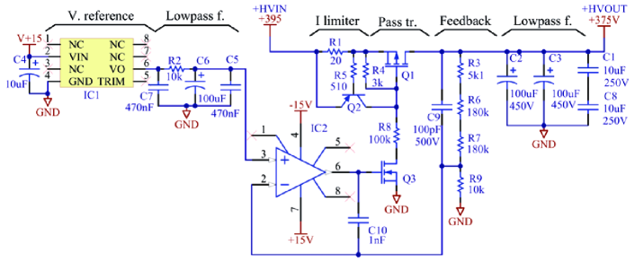
In our case we solve this problem by means of the linear low-dropout regulator circuit Texas Instruments (1999, 2013) shown in Fig. 1 providing a DC voltage output of +375 V. This circuit has a low-noise voltage reference (IC1), a low-pass filter (C5, C6, C7, R2), a low-noise operational amplifier (IC2), and high-voltage transistors (Q1, Q3). The load regulation and ripple of the rectified wave are controlled by the feedback loop between the operational amplifier and the resistors network. The high-voltage source that feeds the circuit comes from a custom-built step-up transformer and a full-wave rectifier bridge with filter capacitors (not shown in the figure) providing +395 V to the regulator. The circuit regulates the output voltage to a fixed value generated by the reference voltage times the feedback gain, with the pass transistor Q1 operating in the active region of the MOSFET Texas Instruments (1999). Adequate values for R4 and R8 must be selected accordingly to the V values of the Q1 transistor and to the leakage currents in the polarization networkTexas Instruments (1999). The efficiency of the circuit is of 85% in normal operation at 30 mA . The main specifications of our power-supply are summarized in table 1.
In order to reduce the power-supply output noise we have chosen the low-noise voltage reference LT1021 providing + 10 V in the regulator with a noise level lower than 1 ppm in 10 Hz and a thermal-drift smaller than 5 ppm/K. The low-pass network was implemented with a cut-off frequency of 1 Hz in order to minimize noise from the reference Maxim (2005); Nogawa (2012). With the aim of reducing the noise introduced in this stage we used a NE5534 operational amplifier. An additional advantage of the low-dropout topology of our circuit is the low power required to polarize the transistors, and the possibility of high output currents with high efficiency Texas Instruments (1999).
The circuit presented here is rather flexible and can be easily adapted to implement power supplies with lower and higher output voltages as well as inverse polarity. A negative voltage-output supply can be implemented with the same elements working in inverse polarity and replacing the MOS-N with a MOS-P transistor, and viceversa Texas Instruments (1999). The absolute value of the voltage output can be increased up to 600 V by conveniently choosing the feedback resistors. The practical limit for the largest absolute voltage output of the source is the maximum VDS across the transistors. For the circuit proposed here the transistors are MOS-P MTP2P50 (Q1) and MOS-N BUZ80A (Q3), withstanding up to 500 and 800 V, respectively. Alternatively, the MOS-P transistor can be replaced by the IXTH16P60P component withstanding a maximum of 600 V and a continuous current of 16 A. Concerning the efficiency of the circuit, if higher power or power-factor are required, a switching converter can be added as a previous stage to step-up the voltage, in place of the rectifier and transformer.
The design of this circuit considered faults due to short-circuit or current overload with the current limit set by R1. In order to tolerate an infinite-time short-circuit the heat-sink of the pass-transistor (Q1) has to be chosen carefully considering that in our design the maximum current is of 30 mA and that the transistor works for voltages smaller than + 375 V. This current limit can be increased up to the maximum drain-source current that for Q1 is of 2 A. For this current-limiting stage, we connected the Q2 transistor in a floating configuration avoiding the use of a high-voltage component.
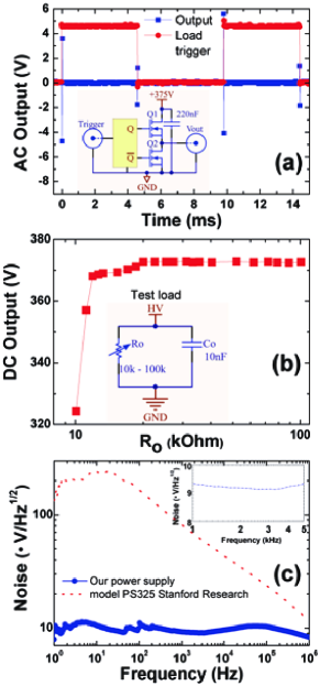
One application of this power supply is the feeding of the control electronics of piezoelectric motors that for coarse motion work normally in a slip-stick mode Chatterjee et al. (2009); Renner et al. (1990). Therefore we tested its stability during the transient regime of a capacitive load of the order of piezoelectric motors excited with asymmetric signals. This was performed by switching on and off the bridge circuit shown in the insert to Fig. 2(a), connected between the source output and a load of 10 nF. The main panel of Fig. 2(a) shows the transient and stationary response at 100 Hz. On switching on and off the circuit a voltage spike of only % of the nominal output develops. Similar results are obtained up to 10 kHz. This response is due to the abrupt discharge of the capacitors of the source. This figure of merit is reasonably good in order to abruptly charge and discharge a piezoelectric motor in slip-stick coarse positioning mode.
In addition, we performed a load regulation test by using the load shown in the insert to Fig. 2 (b). The evolution of the output voltage on varying the resistor is shown in the main panel of the same figure. In the normal operation regime, the output voltage is within 0.03 % of the nominal value. The mean voltage in normal operation is 372.6 V yielding an accuracy of 0,64 %. For impedances k the maximum output current is reached and the output voltage drops drastically.
The noise in the output voltage has been characterized with a digital-signal-processing lock-in amplifier. The noise spectrum up to 1 MHz is presented in Fig. 2 (c) in the case of a 10 nF load in parallel with a 1 M resistor. The output noise level in this large frequency range is below 12 V/. The noise spectrum integrated in the 100 kHz bandwidth yields an output noise lower than 2 mVpeak. This noise level is one order of magnitude better than relatively expensive commercially-available external high-voltage power supplies such as model PS325 of Stanford Research Stanford Research (2011) (see dotted line in Fig. 2). Our power supply was successfully integrated onto the control electronics Belussi, Gómez Berisso, and Fasano (2013) that drives a scanning probe piezoelectric motor with sub-Angstrom resolution.
The figures of merit and specifications of the circuit presented here makes it a suitable choice to feed actuators, sensors, or to power other high-voltage electronics in order to perform on low-noise level laboratory experiments. Our circuit is based in MOSFET technology components available in any local market that can be easily and suitably replaced in order to provide different polarities as well as output voltage and current values. In conclusion, the circuit presented here is a simple, easy-accessible and flexible custom-built solution for high-voltage low noise level power supplies to be integrated onto control electronics for nanopositioning applications.
References
- Pohl (1987) D. W. Pohl, Rev. Sci. Instrum. 58, 54 (1987).
- Chen et al. (1992) X. Chen, B. Cousins, M. McEllistrem, and R. J. Hamers, Rev. Sci. Instrum. 63, 4308 (1992).
- Usher and McAuley (1993) T. D. Usher and G. a. McAuley, Rev. Sci. Instrum. 64, 2027 (1993).
- Colclough (2000) M. S. Colclough, Rev. Sci. Instrum. 71, 4323 (2000).
- Müller (2005) H. Müller, Rev. Sci. Instrum. 76, 084701 (2005).
- Flaxer (2006) E. Flaxer, Mechatronics 16, 303 (2006).
- Chen et al. (2012) L. Chen, S. H. Kim, A. K. H. Lee, and A. de Lozanne, Rev. Sci. Instrum. 83, 013708 (2012).
- Belussi, Gómez Berisso, and Fasano (2013) C. H. Belussi, M. Gómez Berisso, and Y. Fasano, Rev. Sci. Instrum. 84, 056104 (2013).
- Apex Analog (2013) Apex Analog, “Apex operational Amplifiers,” Tech. Rep. (Apex Analog, 2013).
- Flaxer (2008) E. Flaxer, Rev. Sci. Instrum. 79, 035104 (2008).
- Ertl, Kolar, and Zach (1997) H. Ertl, J. Kolar, and F. Zach, IEEE Trans. Ind. Electron. 44, 116 (1997).
- Koçum (2011) C. Koçum, Rev. Sci. Instrum. 82, 084702 (2011).
- Williams (2008) J. Williams, “High Voltage , Low Noise , DC/DC Converters,” Tech. Rep. March (Linear Technology, 2008).
- Beck (2008) J. Beck, “Using Rectifiers in Voltage Multiplier Circuits Vishay General Semiconductor,” Tech. Rep. (Vishay, 2008).
- Texas Instruments (1999) Texas Instruments, “Technical Review of Low Dropout Voltage Regulator Operation and Performance Application Report,” Tech. Rep. August (Texas Instruments, 1999).
- Texas Instruments (2013) Texas Instruments, “LDO Regulator Stability Using Ceramic Output Capacitors,” Tech. Rep. April (Texas Instruments, 2013).
- Maxim (2005) Maxim, “Ultra-Low-Noise LDO Achieves 6nV / Sqrt Hz Noise Performance,” Tech. Rep. (Maxim, 2005).
- Nogawa (2012) B. M. Nogawa, “LDO noise examined in detail,” Tech. Rep. 1 (Texas Instruments, 2012).
- Chatterjee et al. (2009) K. Chatterjee, M. C. Boyer, W. D. Wise, and E. W. Hudson, Rev. Sci. Instrum. 80, 095110 (2009).
- Renner et al. (1990) C. Renner, P. Niedermann, a. D. Kent, and O. Fischer, Rev. Sci. Instrum. 61, 965 (1990).
- Stanford Research (2011) Stanford Research, “High Voltage Power Supplies,” Tech. Rep. 408 (Stanford Research, 2011).