Revisit the spin-FET: Multiple reflections, inelastic scattering, and lateral size effects
Abstract
We revisit the spin-injected field effect transistor (spin-FET) by simulating a lattice model based on recursive lattice Green’s function approach. In the one-dimensional case and coherent regime, the simulated results reveal noticeable differences from the celebrated Datta-Das model, which motivate thus an improved treatment and lead to analytic and generalized result. The simulation also allows us to address inelastic scattering (using Büttiker’s fictitious reservoir approach) and lateral confinement effects on the control of spins which are important issues in the spin-FET device.
I Introduction
The spin-valve device Ju75 ; Slon89 ; Mood95 and spin-injected field effect transistor (spin-FET) DD90 lie at the heart of spintronics. The basic principle of this type of devices is modulating the resistance by controlling the spins of the carriers Wolf01 ; Zu04 , in particular employing two ferromagnetic (FM) leads as polarization generator and detector. In practice, there existed two major challenges: (i) spin-polarized injection into a semiconducting channel, and (ii) gate control of the Rashba spin-orbit coupling (SOC) in the channel. The former difficulty has been largely overcome through efforts of many groups Rash00 ; Fert01 ; Smi01 ; Bau05 . For the latter issue, investigations included the gate-voltage-controlling of the spin precession in both the quantum wells Nit97 and quantum wires Eng97 , and some detailed studies such as the multichannel mixing effects (lateral size effects) Pa02 ; Go04 ; Ni05 ; Je06 ; Liu06 ; Ge10 ; Pala04 ; Ag10 . Integrating the ingredients of the two types mentioned above into a single device using AsIn heterostructure with a top gate was realized in a recent experiment KK09 . This progress, remarkably, has renewed the interest in the spin-FET device Ge10 ; Ag10 ; Ge10a ; Dat11 , which was proposed for some time longer than two decades by Datta and Das DD90 .
In this work we revisit this novel spintronic device, based on the powerful recursive lattice Green’s function (GF) simulation on a quantum-wire model (semiconductor nanowire implementation). To reach realistic scales, from the InSb material parameters (which have large Landé factor and strong spin-orbit coupling Kou12 ), we design our simulation size (in longitudinal direction) for the quantum wire with 500 lattice sites (about nm length). We may summarize the present study to step the following advances: (i) In the ideal one-dimensional (1-D) case and coherent regime, the simulated results of the energy-resolved transmission spectrum and the SOC-modulation of the transmission peak reveal interesting differences from the well-known Datta-Das model DD90 . Accordingly, we develop a Fabry-Perot cavity model to obtain an analytic result which generalizes Ref. DD90 , and as well the more recent work Dat11 . (ii) The employed recursive GF technique allows for an efficient simulation for the spatial-motion decoherence effect which, quite indirectly, degrades the control of the spin precession. Of particular interest is that this treatment does not involve any explicit spin-flip mechanisms Dya7172 , but only incorporates the Büttiker phase-breaking model But8688 ; Pas90 ; Li01 to introduce spatial decoherence effect. The simulated result agrees with the temperature dependence observed in experiment KK09 , and substantiates the mesoscopic (coherence) requirement remarked in the Datta-Das proposal DD90 or the non-diffusive (ballistic) criterion Eom11 . (iii) We simulate the effect of lateral confinement by setting 20 and 40 lattice sites for the width of the quantum wire. The results are in consistence with some previous studies based on continuous wave-guide models Pa02 ; Go04 ; Ni05 ; Je06 ; Liu06 ; Ge10 ; Pala04 ; Ag10 , implying that the lateral size, if exceeding certain range (drastically violating the 1-D condition), will influence the functionality of the spin-FET device.
II Model and Methods
The device contains a central region (quantum wire) and two FM leads, described by total Hamiltonian , with
| (1a) | |||
| (1b) | |||
| (1c) | |||
For the sake of simplicity, here we specify these Hamiltonians using 1-D tight-binding lattice model (with lattice sites for the quantum wire), and will present extra explanations when extended to higher dimensions (in Sec. III C). The electronic creation and annihilation operators are abbreviated by a vector form, e.g., and , where labels the lattice site and the spin orientations. The Pauli matrices are introduced as . In the quantum wire Hamiltonian (), and are the tight-binding site energy and hopping amplitude; is the SOC strength. Notice that, when converting to a continuous model, the corresponding SOC strength should be , where is the lattice constant. For the FM leads (), , , and are, respectively, the tight-binding parameters and the FM exchange field. For the wire-lead coupling (), we assume a common coupling amplitude at both sides.
In more detail, the FM exchange field takes the direction of magnetization. For spintronic device such as the spin-valve, the left and right leads should have different magnetization directions, and the device function is realized by tuning one of them. However, for the spin-FET, whose function is tuned by manipulating the spin precession in the central region, we can assume the FM leads magnetized in parallel, e.g., with for a -axis magnetization.
II.1 Inelastic Scattering Model
In this work we will address the important issue of decoherence (inelastic scattering) effect in the spin-FET. Rather than the electron-phonon interactions, which are difficult to treat in large-scale simulation of quantum transports, we would like to employ the simpler but somehow equivalent phenomenological phase-breaking approach proposed by Büttiker But8688 .
The basic idea of this approach is to attach the system (quantum wire) to some additional virtual electronic reservoirs. The transport electron is assumed to partially enter the virtual reservoir, suffer an inelastic scattering in it (then lose the phase information), and return back into the system (to guarantee the conservation of electron numbers). As a consequence, the two partial waves of electron, say, the component that once entered the reservoir and the one having not, do not interfere with each other. Technically, we model the virtual reservoir (coupled to the site of the quantum wire) by a tight-binding chain with Hamiltonian Pas90 ; Li01
| (2) |
and this chain is coupled to the quantum wire through a coupling Hamiltonian
| (3) |
with the coupling strength. In this work, for the quantum wire with (length of nm), we will assume to attach 10 side-reservoirs (so ), which represent a mean-distance of nm between the nearest-neighbor inelastic scatterers. This mean-distance and the coupling strength (), jointly, characterize the decoherence strength But8688 .
II.2 Lattice Green’s Function Method
We will base our simulation on the powerful lattice Green’s function (GF) method, in particular combined with a recursive algorithm Datta95 . For large-scale simulation, this technique can avoid using all the lattice sites as state basis, needing only a piece of the lateral lattice sites for a matrix representation. The longitudinal lattice sites are treated by a recursive algorithm. The great advantage of this treatment is saving the dimension of the representation matrix.
Based on the recursive algorithm, one can calculate the retarded and advanced Green’s functions and obtain the transmission coefficients between any pair of leads (reservoirs) as follows Datta95 ; QF01 ; QF09 :
| (4) |
Here we use () to denote all the reservoirs, including the left and right leads together with the virtual inelastic scattering reservoirs. Formally, , and . is the retarded (advanced) self-energy owing to coupling with the lead (reservoir). In practice, can be easily obtained by surface Green’s function technique, and the full-system Green’s function can be efficiently computed using the recursive algorithm.
Knowing , the entire effective transmission coefficient from the left to the right lead can be straightforwardly obtained through Pas90 ; Li01
| (5) |
Here, and . is the inverse of the matrix with elements , where . Inserting the transmission coefficient into the Landauer-type formula, one can easily compute the transport current. In this work, however, we will simply use (corresponding to differential conductance) to characterize the modulation effects in the spin-FET.
III Results and Discussions
In our simulation, for the central quantum wire, we refer to the SOC strength of the InSb material, . This implies a SOC length . Assuming a lattice constant , we then decide to simulate the 1-D quantum wire with lattice sites (length of nm), in order to be longer than for the purpose of spin-FET. For the tight-binding hopping energy, we assume eV. For the FM leads and the fictitious (inelastic scattering) reservoirs, we assume common hopping parameter in their tight-binding models, i.e., eV. Finally we assume splitting exchange energy eV for the FM leads, and for their coupling to the quantum wire.
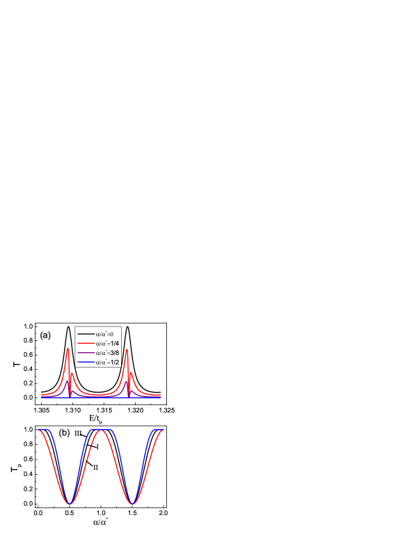
Let us consider first a coherent transport through the quantum wire (corresponding to the case of low temperatures KK09 ). In Fig. 1(a), we display the representative results of the transmission spectrum under the SOC () modulation. Owing to finite length of the quantum wire, the transmission spectrum reveals the usual peak-versus-valley structure. The SOC-induced energy level splitting also results in additional fine-structures (see, for instance, the red curve). In Fig. 1(a) we observe clear SOC-modulation effect on the entire transmission spectrum. For convenience but without loss of physics, in this work we would like to employ the height of the transmission peak to characterize the modulation effect. The extracted results are shown in Fig. 1(b).
We find that the SOC-modulation period is well described by , where . This is in perfect agreement with the result from a simple plane-wave-based interference analysis. Following Ref. DD90 , the phase difference caused by the SOC over distance between the spin-up and spin-down components is given by . In order to convert to the lattice model, making replacement (and noting that ), the above is then given by the condition .
However, the SOC-modulation lineshape does not coincide in general with the prediction of the Datta-Das model DD90 . In Ref. DD90 , it was remarked that the SOC-modulation effect is free from energies. However, as we will prove shortly, this is not true. Also, we find different transition behaviors around the (modulation) peaks and valleys: the variation around the peak can be much slower (forming almost a “plateau”) than the change around the valley. Below we present a semi-quantitative analysis based on essentially the same Datta-Das model but accounting for multiple reflections in the SOC region, which desirably generalizes the central result in Ref. DD90 . We notice also that this type of multiple reflections were not taken into account when fitting and analyzing the experimental result KK09 ; Eom11 ; Dat11 .
III.1 Semi-quantitative Analysis
Let us consider a 1-D continuous model for the quantum wire embedded in between two FM leads. This is similar to an optical two-sided Fabry-Perot cavity system, with the electron transmission as an analog of optical wave. Of particular interest in the electronic setup of spin-FET is the SOC-modulation in the “cavity”, which is described by the continuous version of the Rashba model as , owing to the 1-D motion with . As in the lattice model, we assume the FM leads polarized in -direction. Following the analysis of Datta and Das DD90 , the state of the injected electron is decomposed in superposition of the -eigenstates: (actually in this special case). Then, after a single passage through the (SOC) 1-D wire (forward propagation over distance ), the state evolves to . Here are given by the solution from , for a given energy note-1 .
From a different perspective, in the representation, this evolution manifests an effect of spin precession with angle . Taking into account the role of the FM leads, a transmission coefficient was proposed in Ref. DD90 as . In practice KK09 , this result has been applied to analyze experiment as follows: the measurement voltage, which is proportional to the transmission coefficient, is fitted with , where and are two fitting parameters. In a more recent work Dat11 , deeper analysis was carried out for these two parameters (amplitude and phase), and some aspects of the experiment were explained while some others remained unclear.
A drawback in the above analysis is the neglect of the (infinitely) multiple reflections, which actually exist in any two-leads connected electronic devices. In terms of wave-mechanics treatment, this is exactly the same as the optical two-sided Fabry-Perot cavity. In addition to the forward propagation (spin precession caused by the SOC), one can similarly account for the spin precession in the backward propagation (after reflection at the junction connected with the lead). Particularly, as accounting for the multiple reflections, one should adopt a full reflection for the anti-parallel spin component (with respect to the FM polarization), and the usual transmission and reflection for the component of parallel orientation. As a result, after each reflection at the junction connected with the FM lead, the reflected electron would suffer an amount of spin rotation. After some algebra (summarized in Appendix A), the final result reads
| (6) |
In this result we have denoted and . For the contact of the quantum wire with the FM leads, we assumed identical transmission () and reflection () amplitudes at the two sides. We may remark that, after accounting for the (infinite) multiple reflections, Eq. (6) generalizes the result of Ref. DD90 , elegantly.
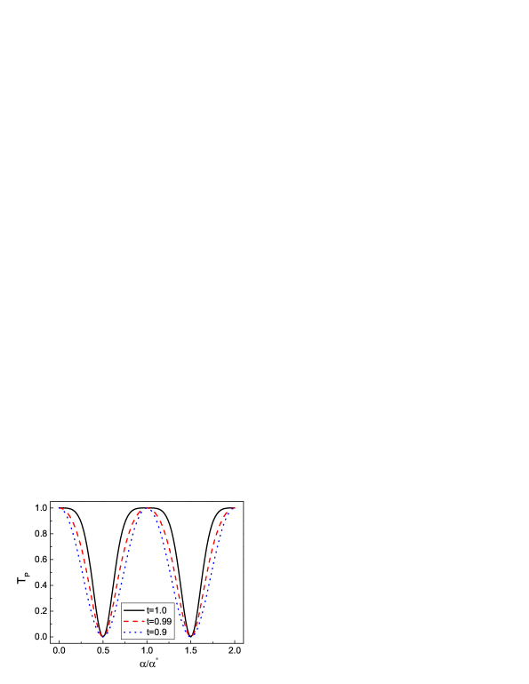
Based on Eq. (6) we show in Fig. 2 the SOC-modulation effect on the (resonant) transmission peak. Interestingly, we find similar lineshape as in Fig. 1(b). In particular, different transition behaviors are found around the peak (maximum) and dip (minimum), for the case . From Eq. (6) and setting , we obtain . This result, in a simple way, allows us to explain the “plateau” behavior of in Fig. 2.
We find in Fig. 2 that, with the decrease of , the transmission peak modulation given by Eq. (6) approximately coincides with the energy-independent modulation predicted in Ref. DD90 . This feature should deserve particular attention, since it may mask the effect of multiple reflections. From Eq. (6), under the condition , an extremal analysis gives the height of the transmission peak as
| (7) |
We see that, with the decrease of (from unity), will soon be close to . For instance, for the still relatively large , one can check . This will make the effect of the second term in the square brackets in Eq. (7) negligible (when is smaller than certain values), as observed in Fig. 2.
Shown in Fig. 2 is only the SOC-modulation effect on the transmission peak. For the entire transmission spectrum, given by Eq. (6), it is clear that the modulation effect depends on energies, through the -dependence. This will more dramatically affect the finite-bias current through the spin-FET, compared with the energy-independent modulation effect DD90 . In Ref. DD90 , it was highlighted that the energy-independent modulation “property”, observed from the differential phase shift , implies an important advantage for quantum-interference device applications. That is, it can avoid washing out the interference effects and achieve large percentage modulation of the current, even in multimoded devices operated at elevated temperatures and large applied bias DD90 . It seems of interest to perform further examination on these statements based on Eq. (6).
Using Eq. (6), one may qualitatively understand the modulation behavior in Fig. 1(b). Compared the lattice system described by Eq. (1) with the Fabry-Perot cavity model, an obvious difference is that the former does not have a constant single-side transmission () and reflection (), where the effective and should depend on the energy () and the SOC . Therefore, from Eq. (6), the transmission peak may have different height in different energy region and may depend on through the effective and . In addition to the multiple reflections, this should be the reason that lead to the non-overlapped modulation lineshapes in different energy areas and the “plateau” behavior around the modulation peak, as shown in Fig. 1(b).
III.2 Decoherence Effect
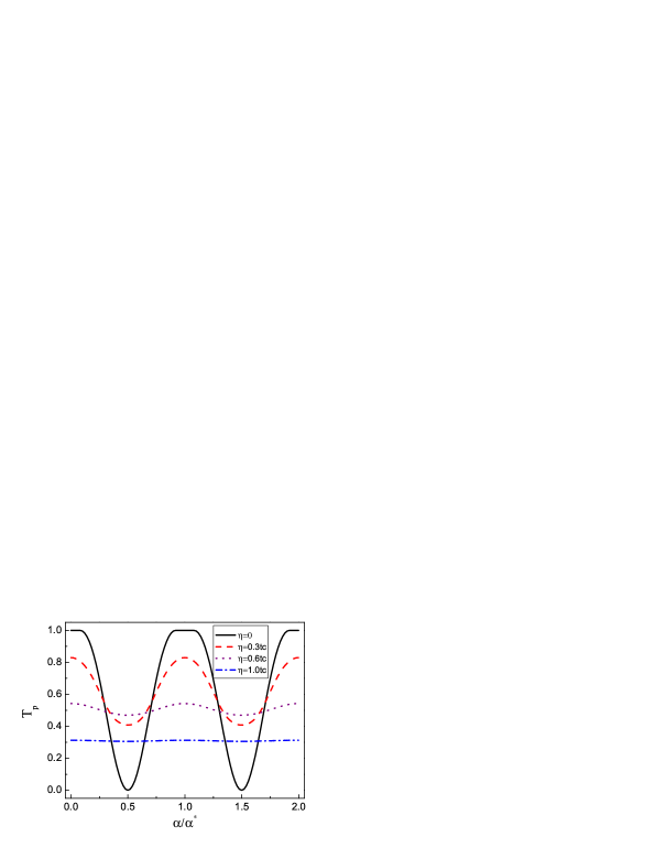
In Fig. 3 we show decoherence effect on the SOC-modulation, using the Büttiker phase-breaking model as briefly outlined in Sec. II A. This phenomenological approach is very efficient compared to any other microscopic model based treatments. However, from Eq. (5), we see that we need to calculate all the , based on Eq. (4). For each , we need to recursively calculate the (full system) Green’s function from the reservoir to the one. It will be very computationally expensive. In practice, however, one can design smart algorithm to avoid this type of repeated recursive computations.
Qualitatively speaking, the inelastic scatterers would cause a large number of forward and backward propagation pathways. Simple analysis in terms of time-reversal symmetry tells us that the forward and backward propagation over equal distance would cancel the spin precession. As a result, for any transmitted electron (from the left to the right leads), the net distance of spin precession is the length of the quantum wire. This explains the common SOC-modulation period () in Fig. 3 when altering the inelastic scattering strength ().
However, the SOC-modulation amplitude will be suppressed by enhancing the inelastic scattering strength. The fictitious reservoir model is very convenient to account for phase breaking (decoherence) of spatial motion, through destroying quantum interference between partial waves. Nevertheless, to the SOC caused spin precession, the role of this model is not so straightforward. We may remark that in our treatment we did not introduce explicit spin-relaxation mechanism Dya7172 , whose effect is relatively more direct Dat11 ; Eom11 . In Ref. DD90 , Datta and Das pointed out that, in order to perform the spin-FET, one of the essential requirements is the central conducting channel within a mesoscopic phase-coherent regime. Our result in Fig. 3 substantiates this requirement, and as well the general remark that the Rashba-spin-control does not work in diffusive transport regime Eom11 . The present result is also in agreement with the experiment KK09 , where the SOC modulation effect was found to be washed out with stronger inelastic scattering (more phonon excitations) by increasing the temperatures.
III.3 Lateral-Size Effect
In the original proposal the intersubband coupling effect owing to lateral size was excluded for a narrow (quasi-1D) quantum wire DD90 . Below, employing the recursive lattice GF approach, we simulate the lateral-size effect by considering a quasi-two-dimensional (2D) quantum ribbon with lattice sites. Accordingly, we need to generalize each lattice site of the 1-D wire to a lateral column with sites along the -direction. While the 2D generalization of the tight-binding model is straightforward, we only specify the SOC Hamiltonian in 2D case as
| (8) |
Here, the summation is over the lattice sites, and denote displacements over a unit lattice cell along the longitudinal () and lateral () directions.
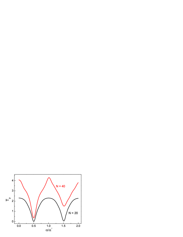
In Fig. 4 we show the effects of the lateral size (with and ). First, owing to the energy sub-bands (and their mixing) caused by the lateral confinement, the transmission peak can exceed unity (in the 1-D case the maximal is unity). One may notice that, unlike prediction from the standard Landauer-Büttiker formula, the height of the transmission peak, which is proportional to the differential conductance at the corresponding energy (bias), does not equal the lateral-channel numbers involved. In 1-D case, the transmission peak is originated from a constructive interference given by the standing-wave condition of the longitudinal wave-vector. This resonant condition (together with symmetric coupling to the leads) will result in a transmission coefficient of unity. However, for a given energy () in the quantum-ribbon system, different lateral channels are associated with different longitudinal wave-vectors. Then, the resonant condition for each transverse channel cannot be satisfied simultaneously.
The second effect originated from the lateral motion is the SOC-induced additional spin precession. In general, this will affect the SOC-modulation quality of the spin-FET. For small (with respect to the SOC length with sites in the present study), this effect is not prominent (see, for instance, the result of in Fig. 4). However, with the increase of the lateral size, the transmission cannot be switched off (particularly at higher ), as illustrated by the result of . Moreover (not shown in Fig. 4), with even larger lateral-size and SOC-, or in some energy domain, the transmission modulation will become strongly irregular. We then conclude that, while the longitudinal modulation period () keeps unchanged, the quality of the spin-FET performance will be degraded with the increase of the lateral size. Only for narrow quantum wire (small ) and relatively weak , one can define desirable working region for the spin-FET. This remark supports the conclusion in Ref. Ge10 , and some previous studies Pa02 ; Go04 ; Ni05 ; Je06 ; Liu06 . It seems that an exception is the 2D system with semi-infinite (considerably wide) width, where the SOC modulation effect, despite of the degraded quality, can be restored Pala04 ; Ag10 ; Dat11 ; Eom11 .
IV Summary
We have revisited the transport rooted in the spin-FET device, with the help of the powerful recursive lattice Green’s function approach. Our result of the energy-resolved transmission spectrum reveals noticeable differences from the Datta-Das model DD90 , which motivated us to develop a Fabry-Perot-cavity type treatment to generalize the central result. We also simulated the decoherence and lateral-size effects. The former substantiates the mesoscopic (coherence) requirement DD90 or the non-diffusive (ballistic) criterion Eom11 , and is in reasonable agreement with the observation in the recent experiment KK09 . The latter implies additional restrictions to the Rashba-spin-control and thus the quality of the device.
Acknowledgments— This work was supported by the Major State Basic Research Project of China (Nos. 2011CB808502 & 2012CB932704) and the NNSF of China (No. 91321106).
Appendix A Multiple Reflection Analysis
Following the Fabry-Perot cavity model explained in Sec. III A, let us consider the transmission and reflection of an electron at the right FM lead, which entered from the left FM lead with a wave function (after passing through the left contact junction):
| (9) |
At the right side of the 1-D wire (cavity), after single passage (over ) under the SOC influence, the electron state evolves to
| (12) | |||||
Here and in the following, using the transfer matrix representation, the states should be understood as column vectors in the basis , e.g., . For a given energy , are solved from , corresponding to the momentums of the spin-up and spin-down electrons.
Since the FM leads are polarized in the -direction, at the right side, only the electron with spin state can enter the right lead (with transmission amplitude and reflection amplitude ). For electron with , it will be fully reflected. Accordingly, based on , the transmitted wave into the right lead is given by
| (13) |
In this context we introduce the projection operators
| (14) |
In Eq. (13) we also defined a transfer matrix which reads
| (17) |
At the same time, the reflected wave from the right junction is given by
| (18) |
where
| (21) |
Similar analysis gives the transfer matrix acting on the wave inversely propagated from the right side to the left one and reflected at the left junction:
| (24) |
Therefor, the total wave arriving to the right FM lead is a sum of all the partial waves, given by
| (25) | |||||
Noting that , we finally obtain the total transmission probability as
| (26) |
Here we defined and , and introduced .
References
- (1) M. Julliére, Phys. Lett. A 54, 225 (1975).
- (2) J. C. Slonczewski, Phys. Rev. B 39, 6995 (1989).
- (3) J. S. Moodera, L. R. Kinder, T. M. Wong, and R. Meservey, Phys. Rev. Lett. 74, 3273 (1995).
- (4) S. Datta and B. Das, Appl. Phys. Lett. 56, 665 (1990).
- (5) S. A. Wolf et al., Science 294, 1488 (2001).
- (6) I. Zutic, J. Fabian, and S. Das Sarma, Rev. Mod. Phys. 76, 323 (2004).
- (7) E. I. Rashba, Phys. Rev. B 62, R16267 (2000).
- (8) A. Fert and H. Jaffres, Phys. Rev. B 64, 184420 (2001).
- (9) D. L. Smith and R. N. Silver, Phys. Rev. B 64, 045323 (2001).
- (10) G. E. W. Bauer, Y. Tserkovnyak, A. Brataas, J. Ren, K. Xia, M. Zwierzycki, and P. J. Kelly, Phys. Rev. B 72, 155304 (2005).
- (11) J. Nitta, T. Akazaki, H. Takayanagi and T. Enoki, Phys. Rev. Lett. 78, 1335 (1997).
- (12) G. Engels, J. Lange, T. Schäpers and H. Lüth, 1997 Phys. Rev. B 55, R1958 (1997).
- (13) T. P. Pareek and P. Bruno, Phys. Rev. B 65, 241305 (2002).
- (14) M. Governale and U. Zülicke, Solid State Commun. 131, 581 (2004).
- (15) B. K. Nikolic and S. Souma, Phys. Rev. B 71, 195328 (2005).
- (16) J. S. Jeong and H. W. Lee, Phys. Rev. B 74, 195311 (2006).
- (17) M.-H. Liu and C.-R. Chang, Phys. Rev. B 73, 205301 (2006).
- (18) M. M. Gelabert, L. Serra, D. Sanchez, and R. Lopez, Phys. Rev. B 81, 165317 (2010).
- (19) M. G. Pala, M. Governale, J. König, and U. Zülicke, Europhys. Lett. 65, 850 (2004).
- (20) P. Agnihotri and S. Bandyopadhyay, Physica E 42, 1736 (2010).
- (21) H. C. Koo, J. H. Kwon, J. Eom, J. Chang, S. H. Han, and M. Johnson, Science 325, 1515 (2009).
- (22) M. M. Gelabert and L. Serra, ArXiv:1005.2480 (unpublished).
- (23) A. N. M. Zainuddin, S. Hong, L. Siddiqui and S. Datta, Phys. Rev. B 84, 165306 (2011).
- (24) J. Eom, H. C. Koo, J. Chang, and S. H. Han, Current Appl. Phys. 11, 276-279 (2011).
- (25) V. Mourik et al., Science 336, 1003 (2012).
- (26) M. I. D’yakonov and V. I. Perel, Sov. Phys. JETP 33, 1053 (1971); Sov. Phys. Solid State 13, 3023 (1972).
- (27) M. Büttiker, Phys. Rev. B 33, 3020 (1986); IBM J. Res. Dev. 32, 63 (1988).
- (28) J. L. D’Amato and H. M. Pastawski, Phys. Rev. B 41, 7411 (1990).
- (29) X. Q. Li and Y. J. Yan, J. Chem. Phys. 115, 4169 (2001); Appl. Phys. Lett. 79, 2190 (2001).
- (30) S. Datta, Electronic Transport in Mesoscopic Systems (Cambridge University Press, Cambridge, U.K. 1995).
- (31) Y. Zhu, Q. F. Sun, and T. H. Lin, Phys. Rev. B 65, 024516 (2001).
- (32) Q. F. Sun and X. C. Xie, J. Phys.: Condens. Matter 21, 344204 (2009).
- (33) For an 1-D lattice model, can be solved from , giving . This result indicates, as the same as the 1-D continuous model, that the spin precession angle is independent of the energy.
- (34) For the result of , our numerical accuracy is not high enough to allow us to precisely determine the (resonant) transmission peaks, owing to the extremely dense energy levels (with actually energy levels of the system). This makes the SOC()-modulation curve of in Fig. 4 not very satisfactory. But this imperfect result may not affect the main underlying physics (effect).