Thermoelectric Corrections to Quantum Voltage Measurement
Abstract
A generalization of Büttiker’s voltage probe concept for nonzero temperatures is an open third terminal of a quantum thermoelectric circuit. An explicit analytic expression for the thermoelectric correction to an ideal quantum voltage measurement is derived, and interpreted in terms of local Peltier cooling/heating within the nonequilibrium system. The thermoelectric correction is found to be large (up to of the peak voltage) in a prototypical ballistic quantum conductor (graphene nanoribbon). The effects of measurement non-ideality are also investigated. Our findings have important implications for precision local electrical measurements.
Following the work of Engquist and Anderson Engquist and Anderson (1981), Markus Büttiker developed a paradigm Büttiker (1988, 1989); Förster et al. (2007) of quantum voltage measurement carried out by a probe consisting of a reservoir of non-interacting electrons coupled locally to a system of interest. The probe exchanges electrons with the system until it reaches local electrical equilibrium with the system:
| (1) |
where is the mean electrical current flowing into the probe. Once equilibrium is established, the chemical potential of the probe constitutes a measurement of the local electrochemical potential (and voltage ) within the nonequilibrium quantum system Büttiker (1989). The condition (1) implies the probe has a large electrical input impedance, a necessary condition for a faithful voltage measurement. Scanning potentiometers satisfying these conditions Kalinin and Gruverman (2007) are now a mature technology, and many experiments in mesoscopic electrical transport utilize voltage probes as circuit components Benoit et al. (1986); Shepard et al. (1992); de Picciotto et al. (2001); Gao et al. (2005).
Although the average electric current into the probe is zero, electrons are constantly being emitted from the system into the probe, and replaced by electrons from the probe reservoir whose quantum mechanical phase is uncorrelated with those emitted by the system. In this way, such a voltage probe serves as an inelastic scatterer Büttiker (1988). Indeed, much of the theoretical interest in Büttiker’s model of a voltage probe is as a convenient way to introduce inelastic scattering in a quantum coherent conductor at the expense of introducing one additional electrical terminal.
Büttiker’s early analysis Büttiker (1988, 1989) was confined to systems at absolute zero temperature, where thermoelectric effects are absent. Later, voltage probes at finite temperature were considered in the limit where the thermal coupling of the probe to the environment is large, so that the probe remains at ambient temperature despite its coupling to the nonequilibrium quantum system Förster et al. (2007). This limit is consistent with the original analysis of Engquist and Anderson Engquist and Anderson (1981), which did not consider thermoelectric effects.
However, considered as a model of an inelastic scatterer, a voltage probe cannot be a steady-state source or sink of heat Jacquet (2009). This suggests that in generalizing the voltage probe concept Büttiker (1988, 1989) to finite temperatures, the probe should be not only in local electrical equilibrium, but also in local thermal equilibrium with the system:
| (2) |
where is the heat current flowing into the probe. Condition (2) is required for a probe with a large thermal input impedance.
Further support for the additional condition (2) is provided by considering thermoelectric effects in the three-terminal circuit formed by the system with source, drain, and probe. Even if both source and drain electrodes are held at ambient temperature, an electrical bias between source and drain can drive Peltier cooling/heating within the system, resulting in hot and cold spots differing significantly from ambient temperature. If the probe is not allowed to equilibrate thermally with the system under these conditions, a voltage will develop across the system-probe junction due to the Seebeck effect. Then the probe voltage can no longer be interpreted as a measurement of the local electrochemical potential in the system. We thus define an ideal voltage measurement as one satisfying both conditions (1) and (2). A precision voltage measurement thus requires a simultaneous precision temperature measurement.
A significant challenge to achieving such an ideal voltage measurement is posed by thermal coupling of the probe to the environment Majumdar (1999); Kim et al. (2012); Bergfield et al. (2013, 2013), including to the system’s lattice Förster et al. (2007), which may not be in local thermal equilibrium with the nonequilibrium electron system. Furthermore, this coupling may be many times as large as the probe’s local thermal coupling to the system’s electrons Kim et al. (2012); Bergfield et al. (2013, 2013). The probe’s thermal coupling to anything other than the nonequilibrium electron system of interest leads to a deviation of the probe’s voltage from the ideal value associated with the local electrochemical potential of the system, and thus must be considered a non-ideality. The probe’s thermal coupling to the system’s lattice can be minimized when it is operated in the tunneling regime Bergfield et al. (2013), and continued advances in scanning thermal microscopy (SThM) Majumdar (1999); Kim et al. (2011); Yu et al. (2011); Kim et al. (2012); Menges et al. (2012) promise to further reduce the probe’s thermal coupling to the environment.
I Linear thermoelectric response
In the limit of small electric and thermal bias away from the equilibrium temperature and chemical potential , the electric current and heat current flowing into the probe may be expressed as Bergfield et al. (2013)
| (3) |
where are Onsager linear-response coefficients with electrode labels and , and is the thermal conductance between the probe and the ambient environment Bergfield et al. (2013). Eq. (3) is a completely general linear-response formula, and applies to macroscopic systems, mesoscopic systems, nanostructures, etc., including electrons, phonons, and all other degrees of freedom, with arbitrary interactions between them.
At sufficiently low temperatures or for sufficiently small systems, the electronic contribution to the coefficients may be calculated using elastic quantum transport theory Sivan and Imry (1986); Bergfield and Stafford (2009); Bergfield et al. (2010)
| (4) |
where is the quantum mechanical transmission function Datta (1995) describing the probability to propagate from electrode to electrode , and
| (5) |
is the equilibrium Fermi-Dirac distribution.
I.1 Büttiker’s voltage probe
I.2 Engquist and Anderson’s voltage probe
The question remains, how to generalize Büttiker’s result (7) to systems at non-zero temperatures. Early on, Engquist and Anderson Engquist and Anderson (1981) considered both voltage and temperature probes of quantum electron systems at finite temperature. For the case of a voltage measurement, they assumed the entire system remains at ambient temperature , so that Eqs. (1) and (3) imply
| (8) |
However, substituting Eq. (8) for the probe’s chemical potential into Eq. (3) gives
| (9) |
which is generally non-zero at finite temperature. This is a generic three-terminal thermoelectric effect occuring whenever the probe coupling to the source and drain electrodes (through the system) is unequal. Thus the voltage probe originally proposed by Engquist and Anderson is not in thermal equilibrium with the system. In the absence of thermal equilibrium, the identification of with the local electrochemical potential of the system is problematic, since any temperature differential between sample and probe will lead to a voltage differential through the Seebeck effect. Moreover, the assumption that is inconsistent, given that , unless the thermal coupling of the probe to the environment is so large that the heat current flowing into the probe from the system can be neglected.
II Ideal Voltage Measurement
We define an ideal voltage measurement as one in which the probe is in both electrical and thermal equilibrium with the system. For an electrical bias applied between electrodes 1 and 2, both held at ambient temperature (), Eqs. (1–3) can be solved for the probe voltage of such an ideal measurement, yielding , where the thermoelectric correction to the voltage is
| (10) |
| (11) |
is the thermopower of the probe-sample junction, and is the probe temperature satisfying
| (12) |
where is given by Eq. (9),
| (13) |
is the parallel thermal conductance from electrodes 1 and 2 into the probe, and is the thermal coupling of the probe to the environment at temperature .
III Results
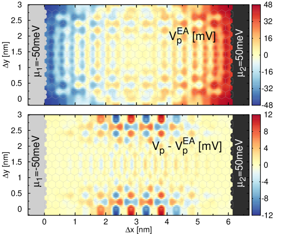
In this section, we calculate the thermoelectric correction to the probe voltage for a prototypical ballistic quantum conductor, a graphene nanoribbon. However, we emphasize that the voltage error induced by thermoelectric effects is a generic phenomenon, and not material specific. Figure 1 shows the computed voltage distribution for a zig-zag graphene nanoribbon with an electrical bias of 0.1V between the source and drain electrodes (at right and left in the figure), which are held at the ambient temperature of . The equilibrium chemical potential of the nanoribbon (determined by doping and/or a backgate) was taken as =-57.5meV. In our calculations, the -system of the graphene nanoribbon is described using a tight-binding model which has been shown to accurately reproduce the low-energy physics of this system Reich et al. (2002). The macroscopic electrodes are assumed to operate in the broad-band limit, where the electrode-nanoribbon coupling is independent of energy, with a per-orbital bonding strength of 2.5eV. The voltage probe is modeled as an atomically-sharp Pt tip scanned at a fixed height of 3Å above the plane of the C nuclei (tunneling regime). The tunneling matrix elements between the probe atoms and the nanoribbon were determined using the methods outlined in Ref. 23. The linear-response coefficients were calculated using Eq. (4) following the methods of Refs. Bergfield et al. (2013, 2013). Additional details of our computational methods may be found in the Supporting Information.
The top panel of Fig. 1 shows the Engquist-Anderson voltage computed from Eq. (8), while the bottom panel shows the thermoelectric correction to the probe voltage, computed from Eqs. (10–13). For this case, which is representative of various geometries we have considered (See Supporting Information), the thermoelectric correction to the measured voltage is of the maxiumum voltage and of the applied bias, highlighting the importance of thermoelectric effects on precision voltage measurements in quantum systems. As mentioned previously, this system is not unique and even larger corrections are expected for systems with larger thermoelectric responses.
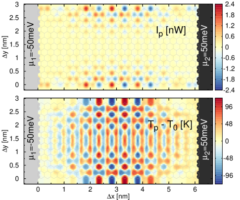
The cause of the substantial thermoelectric correction to the voltage is elucidated in Fig. 2. The top panel of Fig. 2 shows the heat current flowing into the probe when its temperature is held fixed at , calculated using Eq. (9). The peak values of may not be large in an absolute sense, but they correspond to a heat current density of through the apex atom at the tip of the probe, some 700 times the radiant energy flux at the surface of the sun! Clearly, the assumption that such a probe, whose voltage is given by Eq. (8), is in local equilibrium with the system is questionable.
The bottom panel of Fig. 2 shows the deviation of the temperature of an ideal thermoelectric probe from ambient temperature, calculated from Eq. (12). The ideal probe is in local thermal equilibrium with the system, and as such, its temperature maps out the hot and cold regions of the system Bergfield et al. (2013); Meair et al. (2014); Bergfield et al. (2013). The lower panel of Fig. 2 shows clear evidence of Peltier cooling/heating of up to within the system induced by the external electrical bias of 0.1V. The large Peltier effect in this system may be related to giant thermoelectric effects predicted in related -conjugated systems Bergfield and Stafford (2009); Bergfield et al. (2010), where quantum interference effects have been shown to strongly enhance thermoelectricity. However, similar phenomena should occur in other ballistic quantum conductors.
III.1 Effect of thermal coupling of probe to environment
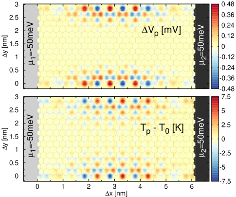
Let us now consider the effects of measurement non-ideality. The greatest source of error in a scanning thermoelectric measurement is likely to stem from the unavoidable coupling of the probe to the thermal background (typically, the ambient environment) Bergfield et al. (2013). Indeed, state-of-the-art SThM still operates in the regime where the coupling of the probe to the thermal background is many times its thermal coupling to the system itself Kim et al. (2012). While values of much less than the thermal conductance quantum (0.284nW/K at 300K) Rego and Kirczenow (1998) are possible in principle for probes whose thermal coupling to the environment is predominantly radiative Bergfield et al. (2013), current scanning probes Kim et al. (2012) have .
Figure 3 shows the thermoelectric correction to the voltage (upper panel) and the probe temperature (lower panel) for . For this case, the thermal coupling of the probe to the environment exceeds its coupling to the system, so that the probe temperature is closer to ambient, and the thermoelectric correction to the voltage is reduced. The reduction of the thermoelectric corrections is described analytically by Eqs. (10) and (12). Even for a thermal coupling of , typical of current state-of-the-art SThM Kim et al. (2012), the voltage error would still be of order 1V, well within the resolution of precision voltage measurements, which routinely obtain sub-Ångstrom spatial resolution Kalinin and Gruverman (2007).
IV Conclusions
An ideal voltage measurement in a nonequilibrium quantum system was defined in terms of a floating thermoelectric probe that reaches both electrical and thermal equilibrium with a system via local (e.g., tunnel) coupling. This definition extends Büttiker’s quantum voltage probe paradigm Büttiker (1988, 1989) to systems at finite temperature, where thermoelectric effects are important.
As an example, we developed a realistic model of a scanning potentiometer with atomic resolution and used it to investigate voltage measurement in a prototypical ballistic quantum conductor (a graphene nanoribbon) bonded to source and drain electrodes. Under ideal measurement conditions, we predict large thermoelectric voltage corrections (24% of the probe’s peak voltage signal) when the applied source-drain bias voltage is small. We also derived expressions for the probe’s voltage correction under non-ideal measurement conditions, finding that the voltage correction is reduced linearly as the probe-environment coupling is increased. In the graphene nanoribbon system considered here, voltage corrections on the order of several V persist even with strong environmental coupling.
In summary, we predict a large thermoelectric correction to voltage measurement in quantum coherent conductors. The origin of this correction is local Peltier cooling/heating within the nonequilibrium quantum system, a generic three-terminal thermoelectric effect. This finding has important implications for precision local electrical measurements: it implies that a precision voltage measurement requires a simultaneous precision temperature measurement.
Acknowledgements.
This paper is dedicated to the memory of Markus Büttiker, whose ideas continue to inspire our quest to understand nonequilibrium quantum systems. C.A.S. was supported by the Department of Energy–Basic Energy Sciences grant no. DE-SC0006699.References
- Engquist and Anderson (1981) H.-L. Engquist and P. W. Anderson, Phys. Rev. B 24, 1151 (1981).
- Büttiker (1988) M. Büttiker, IBM J. Res. Dev. 32, 63 (1988).
- Büttiker (1989) M. Büttiker, Phys. Rev. B 40, 3409 (1989).
- Förster et al. (2007) H. Förster, P. Samuelsson, S. Pilgram, and M. Büttiker, Phys. Rev. B 75, 035340 (2007).
- Kalinin and Gruverman (2007) S. V. Kalinin and A. Gruverman, Scanning probe microscopy: electrical and electromechanical phenomena at the nanoscale, Vol. 1 (Springer, 2007).
- Benoit et al. (1986) A. D. Benoit, S. Washburn, C. P. Umbach, R. B. Laibowitz, and R. A. Webb, Phys. Rev. Lett. 57, 1765 (1986).
- Shepard et al. (1992) K. L. Shepard, M. L. Roukes, and B. P. van der Gaag, Phys. Rev. B 46, 9648 (1992).
- de Picciotto et al. (2001) R. de Picciotto, H. Stormer, L. Pfeiffer, K. Baldwin, and K. West, Nature 411, 51 (2001).
- Gao et al. (2005) B. Gao, Y. F. Chen, M. S. Fuhrer, D. C. Glattli, and A. Bachtold, Phys. Rev. Lett. 95, 196802 (2005).
- Jacquet (2009) P. A. Jacquet, Journal of Statistical Physics 134, 709 (2009).
- Majumdar (1999) A. Majumdar, Annu. Rev. Mater. Sci. 29, 505 (1999).
- Kim et al. (2012) K. Kim, W. Jeong, W. Lee, and P. Reddy, ACS Nano 6, 4248 (2012).
- Bergfield et al. (2013) J. P. Bergfield, S. M. Story, R. C. Stafford, and C. A. Stafford, ACS Nano 7, 4429 (2013).
- Bergfield et al. (2013) J. P. Bergfield, M. A. Ratner, C. A. Stafford, and M. Di Ventra, ArXiv e-prints (2013), arXiv:1305.6602 [cond-mat.mes-hall] .
- Kim et al. (2011) K. Kim, J. Chung, G. Hwang, O. Kwon, and J. S. Lee, ACS Nano 5, 8700 (2011).
- Yu et al. (2011) Y.-J. Yu, M. Y. Han, S. Berciaud, A. B. Georgescu, T. F. Heinz, L. E. Brus, K. S. Kim, and P. Kim, Appl. Phys. Lett. 99, 183105 (2011).
- Menges et al. (2012) F. Menges, H. Riel, A. Stemmer, and B. Gotsmann, Nano Lett. 12, 596 (2012).
- Sivan and Imry (1986) U. Sivan and Y. Imry, Phys. Rev. B 33, 551 (1986).
- Bergfield and Stafford (2009) J. P. Bergfield and C. A. Stafford, Nano Letters 9, 3072 (2009).
- Bergfield et al. (2010) J. P. Bergfield, M. A. Solis, and C. A. Stafford, ACS Nano 4, 5314 (2010).
- Datta (1995) S. Datta, Electronic Transport in Mesoscopic Systems (Cambridge University Press, Cambridge, UK, 1995).
- Reich et al. (2002) S. Reich, J. Maultzsch, C. Thomsen, and P. Ordejon, Phys. Rev. B 66, 035412 (2002).
- Chen (1993) C. J. Chen, Introduction to Scanning Tunneling Microscopy, 2nd ed. (Oxford University Press, New York, 1993).
- Meair et al. (2014) J. Meair, J. P. Bergfield, C. A. Stafford, and P. Jacquod, Phys. Rev. B 90, 035407 (2014).
- Rego and Kirczenow (1998) L. G. C. Rego and G. Kirczenow, Physical Review Letters 81, 232 (1998).