Graphene vertical hot-electron terahertz detectors
Abstract
We propose and analyze the concept of the vertical hot-electron terahertz (THz) graphene-layer detectors (GLDs) based on the double-GL and multiple-GL structures with the barrier layers made of materials with a moderate conduction band off-set (such as tungsten disulfide and related materials). The operation of these detectors is enabled by the thermionic emissions from the GLs enhanced by the electrons heated by incoming THz radiation. Hence, Hence, these detectors are the hot-electron bolometric detectors. The electron heating is primarily associated with the intraband absorption (the Drude absorption). In the frame of the developed model, we calculate the responsivity and detectivity as functions of the photon energy, GL doping, and the applied voltage for the GL detectors (GLDs) with different number of GLs. The detectors based on the cascade multiple-GL structures can exhibit a substantial photoelectric gain resulting in the elevated responsivity and detectivity. The advantages of the THz detectors under consideration are associated with their high sensitivity to the normal incident radiation and efficient operation at room temperature at the low end of the THz frequency range. Such GLDs with a metal grating, supporting the excitation of plasma oscillations in the GL-structures by the incident THz radiation, can exhibit a strong resonant response at the frequencies of several THz (in the range, where the operation of the conventional detectors based on A3B5 materials, in particular THz quantum-well detectors, is hindered due to a strong optical phonon radiation absorption in such materials). We also evaluate also the characteristics of GLDs in the mid- and far-infrared ranges where the electron heating is due to the interband absorption in GLs.
I Introduction
The gapless energy spectrum of graphene 1 enables using single- or multiple graphene-layer (GL) structures for different terahertz (THz) and infrared (IR) photodetectors based on involving the interband transitions 1 ; 2 ; 3 ; 4 ; 5 ; 6 ; 7 (see, also Refs 8 ; 9 ; 10 ; 11 ; 12 ; 13 ; 14 ; 15 ; 16 ; 17 ; 18 ), where different THz and IR photodetectors based on GLs were explored). The interband photodetectors use either the GLs serving as photoconductors or the lateral p-i-n junctions. In the latter case, the electrons and holes are generated in the depleted i-region and move to the opposite GL contacts driven by the electric field in the depletion region 3 . The multiple-GL structures with the lateral p-i-n junctions can consist of either several non-Bernal stacked twisted) GLs as in Ref. 3 or GLs separated by the barrier layers such as thin layers of Boron Nitride (hBN), Tungsten Disulfide (WS2), or similar materials. Such heterostructures have recently attracted a considerable interest and enabled several novel devices being proposed and realized 19 ; 20 ; 21 ; 22 ; 23 ; 24 ; 25 ; 26 ; 27 ; 28 ; 29 ; 30 ; 31 . The GL-photodetectors, especially those based on the multiple-GL structures, can combine a high responsivity with a relatively low dark current at elevated temperatures (up to room temperatures). This is because the dark current in the photodetectors in question is mainly determined by the absorption of the optical phonons. Since the optical phonon energy in GLs is rather large (about 0.2 eV), the number of optical phonons is small even at the room temperature. This results in a low thermal generation rate. The mechanisms of the thermal generation associated with the absorption of the acoustic phonons and the Auger processes are forbidden due to the features of the GL energy spectrum. However, the interband tunneling in strong lateral electric fields in the i-region can lead to an enhanced generation of the electron-hole pairs and an elevated dark current limiting the photodetector detectivity 4 . Effective THz detection can be achieved in the lateral diodes with the absorbing GL source and drain sections separated by an array of grapnene nanoribbons (GNRs), which form the potential barriers for hot electrons injected from the source to the drain 22 . As shown in this paper, an effective THz detection can be achieved in the photodetectors based on double-GL and cascade multiple-GL structures with the vertical transport of hot electrons over the barrier layers. We propose and evaluate such THz detectors operating in the regime of the thermionic emission of hot electrons from GLs and their vertical transport over the barrier layers. The advantages of the THz detectors under consideration include high responsivity and detectivity in a wide spectral range at room temperature and a relatively high-speed operation.
The paper is organized as follows. In Sec. II, we discuss the device structures under consideration and the GLD operation principle. Section III deals with general formulas for the dark current and photocurrent associated with the thermionic emission of electrons from GL and controlled by their capture into GLs. In Sec. IV, we calculate the variations of the electron temperature in GLs cause by the intraband (Drude) absorption of the incident THz radiation. In Sections V and VI, using the formulas obtained in Sections III and IV, we derive the expressions for the GLD responsivity and dark-current-limited detectivity, respectively. In Sec. VII, we discuss how the electron capture in the GLs affects the GLD responsivity and detectivity. In Sec. VIII, we consider the possibility to use the plasmonic resonances and get an enhanced response at elevated frequencies. Section IX deals with the analysis of the limitations of our model. In Sec. X we evaluate the GLD operation in the IR spectral range and compare GLDs with some other photodetectors. In Conclusions, we summarize the main results of the paper. The Appendix deals with the heat removal problem
II Device structures and principle of operation
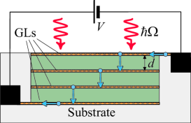
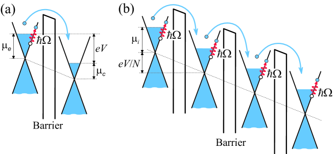
We consider two types of the GLDs: (a) based on the n-doped double-GL structure and (b) n-doped multiple-GL structure with the GLs separated by the barrier layers made of WS2 or similar material with a relatively small conduction band off-set. As an example, Fig. 1 shows a GLD using a four-GL structure. The double-GLDs consist of only the top and bottom GLs serving as the emitter and collector, respectively (no inner GLs). In the multiple-GLDs, the inner GLs clad by the emitter and collector GLs are disconnected from the contacts. In the double-GLDs (with a single barrier), the bias voltage applied between the top and bottom GLs induces the negative electron charge in the emitter GL the equal positive charge in the collector GL. If the equilibrium electron concentration is low and the bias voltage is sufficiently strong, the hole gas will be formed in the collector GL. In GLDs with multiple-GL structures, the inner GLs remain quasi-neutral, so that the electron gas in each GL is formed primarily due the n-type doping, whereas the top and bottom GLs can be charged due to the bias voltage. Figure 2 shows the GLPD band diagrams under the bias. It is assumed that the GLDs under consideration are irradiated by the normally incident THz photons with the energy . The operation of GLDs is associated with the electron heating due to the intraband absorption (Drude absorption) and the interband absorption (see, for example, 32 ) of the incident radiation resulting in an increase of the thermionic current over the barrier layers. Thus, the proposed GLDs are the barrier hot-electron bolometers. In GLDs with the double-GL structures, the electrons entering from the emitter GL and exiting to the collector GL support the lateral current flowing via the contacts, so that the carrier densities in the GLs are maintained. In the multiple-GL structures, the electron density in each GL between the emitter and collector GLs is maintained due to the balance between the electrons leaving and entering GLs via the adjacent barriers due to the thermal emission and the capture processes. If the probability of the capture of an electron crossing a GL is smaller than unity, the GLD operation can exhibit the effect of photoelectric gain. The origin of this gain is of the same nature as in the vertical quantum-well infrared photodetectors (QWIPs) 33 ; 34 ; 35 ; 36 .
The donor density and the bias voltage determine the electron Fermi energies and in the top (emitter) and bottom (collector) GLs, respectively, (, because the bias voltage increases the electron density in the emitting GL and decreases it in the collecting GL). Considering the geometrical and quantum capacitances 37 and taking into account the energy gap between the Dirac points in GLs [see Fig. 2(a)] in the double-GL structure, at relatively low bias voltages one can obtain:
| (1) |
| (2) |
Here , is the electron charge, is the Planck constant, cm/s is the characteristic velocity of electrons and holes in GLs,and and are the dielectric constant and the thickness of the barrier, respectively. At cm-2, and nm, one obtains meV and mV. Relatively large values of imply that for the realistic moderate values of considered in the following, the correction of the Fermi energies in the emitter and collector GLs is small in comparison with . In the multiple-GL structures (with a large number of GLs and the inter-GL barriers ), all the GLs except the top and bottom one’s are quasi-neutral. Although the electrically-induced variation of the Fermi energies in the emitter and collector GLs can be essential (for the mechanism of the photoelectric gain), we will assume that in all GLs, including the top and bottom one’s, the Fermi energies are close to each other and approximately equal to the value determined by the donor density:
| (3) |
III Vertical electron dark current and photocurrent
We restrict our consideration to the double- and multiple-GL structures with relatively thick inter-GL barriers, so that the tunneling current between the GLs can be neglected (the pertinent calculations can be done using the approach developed in Refs. 38 ; 39 . We assume that the main contribution to the vertical current is due to the thermoemission of electrons resulting in the inter-GL transitions (producing the dark current). The impinging THz irradiation heats the electron gas in GLs. This leads to an increase in the thermoemission rate intensifying of the inter-GL transitions, and, hence, the vertical current. The direct electron photoemission is insignificant when the energy of photons is smaller than the GL-barrier conduction band off-set (the height of the barrier with respect of the Dirac point). For the GL structures with the WS2 barriers 40 it implies eV. Hence, this inequality is well satisfied for the THz radiation.
The rate of the thermionic emission from a GL (per unit of its area) is given by
| (4) |
where is the effective electron temperature which (under the irradiation) is higher than the lattice temperature ), is the Boltzmann constant, and is the characteristic time of escape from the GLs of the electrons with the energy , , where is the momentum relaxation time. Using Eq. (4) and assuming for simplicity that ( is the voltage drop across the barrier, and taking into account the electrons photoexcited from the emitter and the photoexcited from and captured to the internal GLs (in multiple-GLDs), we find the thermionic current density, :
| (5) |
Here is the probability of the capture of an electron crossing a GL.
In the GL structures with at least one internal GL (and in the multiple-GL structures), the effects of the balance of thermogeneration from and capture to each GL, are taken into account by introducing the capture probability , as in the standard models of QWIPs 33 ; 34 ; 35 ; 36 . In such an approach, the rate of the electron capture into each GL is equal to . Equating the capture rate and the thermogeneration rate , one obtains [Eq. (5)]. The quantity can be relatively large if the capture probability is small. This quantity essentially determines the dark current and photocurrent gain .
Equation (5) yields the following formula for the current density without irradiation (i.e., for the dark current) when the dark electron temperature is equal to the lattice temperature :
| (6) |
In the double-GLDs all the electrons generated by the emitter GL are captured by the collector GL, so that in such a case .
Considering the variation of the electron temperature , the photocurrent density can be presented as
| (7) |
IV Electron heating by incoming THz radiation
As previously 22 ; 32 , we assume that the electron energy relaxation is associated with the processes of the emission and absorption of optical phonons. In this case, for the rate, , of the energy transfer from the electron system to the optical phonon system is determined by (see, for example, 22 ; 32 ):
| (8) |
Here and are the energy and the number of optical phonons, respectively, is the characteristics time of the optical phonon spontaneous emission for the electron energy .
If the characteristic time of the optical phonons decay , is close to its equilibrium value: . In the case of , the effective energy relaxation time should be replaced by (where ) 14 .
When the effective electron temperature in GLs deviates from its equilibrium value (due to the absorption of THz radiation), the energy relaxation rate can be presented as [see Eq. (8)]
| (9) |
The rate of the energy transfer from the electron system to the optical phonon system is equal to the rate, , of the energy transferred from the THz radiation to the electron system:
| (10) |
Considering the intraband, i.e., the so-called free electron absorption (the Drude absorption) and the interband absorption, the net absorption rate can approximately be presented as
| (11) |
Here , is the speed of light in vacuum, is the THz photon flux entering into the device (or the incident photon flux in the case of the anti-reflection coating), and
| (12) |
is the Drude weight, the factor determining the contribution of the Drude absorption (it is proportional for the real part of the intraband conductivity of GLs). For the realistic values of , the factor can markedly exceed unity. Indeed, assuming meV and s, one obtains . Strictly speaking, Eq. (11) is valid at not too strong absorption.
Since the Fermi energy in the GLD under consideration should be sufficiently large, the processes of the interband absorption of THz photons (their energy ), corresponding to the second term in Eq. (11), are effectively suppressed due to the Pauli blocking. This implies that the electron heating by THz radiation is primarily associated with the intraband absorption (with the Drude or the so-called free-electron absorption). In Eq. (11) and in the following equations we disregard the attenuation in the multiple-GLDs of the THz photon flux associated with the absorption of in GLs, which are closer to the irradiated surface (emitter). This should be valid at not too large values of .
Taking into account the energy balance in each GL governed by Eq. (10) and using Eq. (11) (omitting the term describing the interband absorption), we arrive to the following expression for the variation of the effective electron energy caused by the THz of IR radiation of moderate intensity:
| (13) |
Equation (13) corresponds to the electron energy relaxation time (determined by the optical phonons), which is equal to 22
| (14) |
V Responsivity
Using Eqs. (6) and (8), for the GLD responsivity , we obtain
| (15) |
Using Eqs. (13) and (15), we arrive at the following expressions for the responsivity:
| (16) |
Here
| (17) |
As seen from Eq. (16), the GLD responsivity is proportional to an exponential factor. To achieve reasonable GLD characteristics, the Fermi energy should not be too small in comparison with the barrier height . One can also see that . As stated above, in the GLDs with the multiple-GL structures, the factor can be fairly large.
Equation (16) describes the GLD responsivity as a function of the THz radiation frequency , the temperature and the GL doping (via the dependence of on ).
Assuming meV, ps, , and for K, from Eq. (17) we obtain from Eq. (17) A/W.
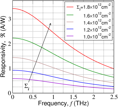
Figure 3 shows the GLD responsivity versus the photon frequency calculated for different donor densities using Eqs. (16) and (17) for meV and the same other parameters as in the above estimate. This corresponds to the GLDs based on the double-GL structure or to the GLDs based on the multiple-GLDs with a strong electron capture in the internal GLs. The responsivity of the latter can be much higher than that shown in Fig. 3 if (see below).
VI Dark current limited detectivity
Considering that the shot noise current (at the value of the signal current equal to the dark current) is given by , where is the bandwidth and is the dark current and photoelectric gain, the dark current limited detectivity (see, for example, Ref. 36 ), can be presented in the following form:
| (18) |
Accounting for Eq. (16), we arrive at
| (19) |
where
| (20) |
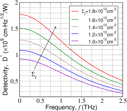
For ps, , ps, ps, and K, meV, cm-2 ( meV), , and THz from Eqs. (19) and (20) we obtain cm Hz1/2/W and cm Hz1/2/W. Figure 4 shows the spectral characteristics of GLDs with cm-2 ( meV) calculated using Eqs. (19) and (20) for the same other parameters as from the latter estimate and Fig. 3.
From Eqs. (16), (17), (19), and (20), one can see that the GLD responsivity is independent on (in the framework of the present model), whereas the GLD detectivity is proportional to (as in QWIPs 36 ).
VII Role of the electron capture
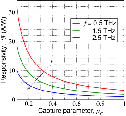
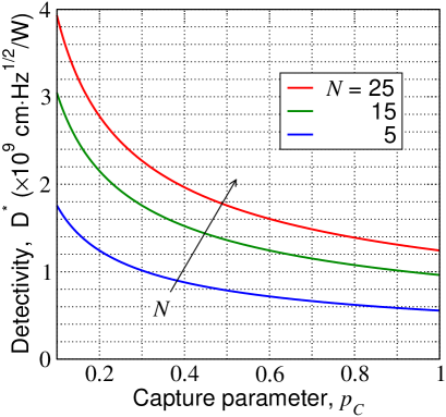
As follows from Eqs. (16), (17), (19), and (20), both the responsivity and detectivity of the multiple GLDs increase with decreasing capture probability , i.e., with increasing photoelectric gain. The latter quantity is determined by several factors, in particular, by the degree of the electron heating in the inter-GL barriers and, hence, by the potential drop across these barriers and their thickness. The detailed calculations of require additional quantum-mechanical calculations of the electron transitions from the continuum states above the barriers to the bound states in GLs coupled with the ensemble Monte Carlo modeling of the electron propagation across the GL-structure similar to that made previously for multiple-QW structures based on the standard semiconductor heterostructures (see, for example, Refs. 35 ; 41 ; 42 ). This is, however, beyond the scope of this work, so that here we consider as a phenomenological parameter. Figures 5 and 6 show the GLD responsivity and detectivity as functions of the capture parameter. One can see that a decrease in the capture parameter leads to a substantial rise of . At low , the GLD responsivity can be fairly high. The detectivity of GLDs with the multiple-GL structure also rises with decreasing as well as with increasing . Since the capture probability in the multiple-GL structures should markedly decrease with increasing electric field in the barrier layers (as in multiple-QWIPs 35 ), the GLD responsivity and detectivity can be rising functions of the bias voltage if the proper heat removal is provided.
VIII Effect of plasmonic resonances
Since the absorption of the incident THz radiation is associated with the Drude mechanism, the absorption efficiency and, hence, the GLD responsivity and detectivity can be relatively small in the frequency range . If ps, this corresponds to THz. However, the operation of GLDs can be extended to much higher frequencies if the GLD structure is supplied by a metal grating over the top GL (not shown in Fig. 1). In this case, the incident THz radiation can result in an efficient excitation of plasma oscillations in the electron-hole system in the double-GL GLDs and in the system of electrons in all GLs (in the multiple-GL structures). Simplifying the equations from Ref. 43 for the GLDs with a metal grating, the rate of the THz radiation absorption at the frequency near the -th plasmon resonance () can be presented as 43 :
| (21) |
Here and are determined by the ratio of the collisional damping (which is actually close to ) and the parameter of the radiative damping 44 . Equation (21) does not contain any geometrical parameters such as the grating period, length of grating strips, and the spacing between the grating and the top GL. These parameters only determine the dependence of the resonant plasma frequencies on the device geometry. This is valid as long as those dimensions are much shorter than the THz radiation wavelength and the net length of the grating is of the same order of magnitude as the wavelength.
The quantities depend on the net electron density in all GLs , the spacing between the top GL and the metal grating , and the period of the grating. The latter determines the ”quantized” wave-number of the excited plasma modes (standing plasma waves). One can put , , the length of the GL-structure in the lateral direction,and is the plasma mode index. For simplicity, one can use the following equation for the frequency of the plasma modes (corresponding to ):
| (22) |
or
| (23) |
The square-root dependence of on appears because the net electron density, which determines the contribution to the self-consistent electric field in the plasma waves by all the GLs is proportional to , whereas the electron fictitious mass in GLs is proportional to (see, for example, Ref. 39 ). Setting meV, m (i.e. m and ), and , from Eq. (23) we obtain THz. If and , the GLD responsivity at the resonance is of the same order of magnitude as at the low edge of the THZ range (see Figs. 3 and 5). Thus, the resonant excitation of plasma oscillations results in a strong absorption of the incident THz radiation and, hence, in elevated values of the GLD responsivity (and detectivity) at relatively high frequencies (several THz). Such GLDs can cover the frequency range THz ( meV), which is not accessible by A3B5-based detectors, in particular, THz quantum-well detectors (QWDs) 46 ; 47 ; 48 .
IX Limitations of the model
The model used in the above calculations some simplifications. These simplifications are: (i) The capture probability is the same for all GLs in the GL-structures; (ii) The thermoassisted tunneling is insignificant; (iii) The heating the Joule heating of the structure.
Since the capture probability depends on the heating of electrons in the barriers, it can be determined on only by the average electric field in the GL-structure but partially by the electric field in the adjacent barriers. In this case, the probability of the electron capture to the particular GL can depend on its index. Such kind of non-locality of the electric-field dependence can lead to more nontrivial spatial distributions (as in QWIPs 41 ; 42 ). However, in the GL-structures with the barrier thickness much smaller than the characteristic energy relaxation length, the pertinent effect should be weak. This justifies the assumption that is a constant (which generally depends on the average electric field).
At sufficiently high bias voltages (much higher than those assumed above), the electron escape from GLs can be associated with the thermoassisted tunneling from the bound states in GLs to the continuum states above the barriers. This tunneling can also be used in double- and multiple-GLDs with the structures similar to those considered above. Since the effective activation energy for this mechanism can be markedly smaller that , GLDs with the thermoassisted tunneling can comprise the barriers with larger conduction band offsets than between GLs and WS2, for example, with the barriers. However, this problem requires a separate consideration.
Above we considered the case of not too low bias voltages (). The Joule power can result in an overheating of the GL structure if is relatively strong. Such an overheating can be avoided either by decreasing (decreasing the GL doping level) or by lowering the bias voltage . In the range of bias voltages , the GLD responsivity and detectivity given by Eqs. (16) and (19) should be multiplied by the factors and , respectively. The transfer to the range of relatively low bias voltages leads to a decrease in the Joule power as , but at the expense of a decrease in the responsivity and detectivity ( and ).
The Joule heating can lead to overheating of GLDs if the Joule power exceeds the maximum heat energy which can be removed from the GLD unit area, , without a substantial heating. This results in the following limitation:
| (24) |
where is the device area. Assuming a typical voltage drop cross the GL-structure to be on the order of 50 - 500 mV and the thermal resistance of the package to be on the order of 10 K/W, we obtain that and the current leading to the ten degrees overheating are equal to 1 W and 2 - 20 A, respectively. For a typical 300m2 device, this corresponds to a fairly reasonable current density of A/cm2. Setting cm-2, ps, and , we obtain A/cm2 (i.e., . Much higher current densities could be achieved with improved heat sinks (see, for example, Ref. 49 ) and/or in the pulsed regime of operation.
X Discussion
tunneling can be based on the materials with larger conduction band offsets than between GLs and WS2.
In principle, GLDs can also effectively operate in the mid- and near-IR ranges. At sufficiently high photon energies, the intraband absorption is negligible, whereas the interband radiative processes, corresponding to the second term in the right-hand side of Eq. (11), can efficiently contribute to the heating of the electron gas in GLs if . In such a case for the photon energies , the GLD responsivity is given by
| (25) |
| (26) |
At cm-2 ( meV), Eqs. (25) and (26) yield the values of the responsivity about 20-30 times smaller than in the range (see Figs. 3 and 5). In particular, at cm-2 , assuming , we obtain rather high values A/W. The GLD detectivity in the mid- and near-IR range , being much lower than in the THz range, can be still relatively high (for room temperature). Note that are independent of the photon energy in its wide range (from meV to 800 meV).
Comparing the GLDs based on the vertical double-GL structure under consideration with the GLDs with a lateral structure and the barrier region consisting of an array of graphene nanoribbons using the electron heating in n-GL contact region, 22 one can see that both types of THz detectors at the room temperature exhibit close spectral characteristics. However, the GLDs with the vertical multiple-GL structure can have much higher responsivity and, especially, detectivity if and .
In principle, room-temperature THz detectors utilizing the thermionic emission of electrons heated by the absorbed THz radiation from QWs can be made of A3B5 or Si-Ge heterostructures. Such detectors on the base of vertical multiple-QW structures were proposed and realized a long time ago(see Refs. 50 and 51 , respectively, as well as a recent paper 52 ). The THz detectors based on lateral structures with the barrier regions formed by the metal gates were also realized 53 ; 54 (see also Ref. 55 ). However, the responsivity and detectivity of GLDs under consideration can be markedly higher than that using the A3B5 multiple-QW structures. Comparing the Drude factor for GL-structures [see Eq. (12)] and the same factor for QW-structures with GaAs QWs, one can find the ratio of these factors at the equal electron density and momentum relaxation time is given by
| (27) |
where and are the effective and fictitious electron masses in QWs and GLs, respectively. For GaAs QWs and GLs with meV, these masses are approximately equal to each other. This implies that the THz power absorbed in QWs and GLs are close. However, the electron energy relaxation time in GLs is longer than that in GaAs-QWs and other standard semiconductor QWs. This is mainly due to relatively large optical phonon energy in GLs. Indeed, using Eq. (14) and assuming that ps at the room temperature we obtain ps, while for GaAs ( meV and ps), InAs ( meV and ps), and InSb ( meV and ps) QWs one obtains , 0.93 and 3.93 ps, respectively. Longer electron energy relaxation time corresponds to more effective heating of the electron gas and, hence, higher responsivity. An other factor promoting higher responsivity (and detectivity) of GLDs is the possibility to achieve higher photoelectric gain due to smaller values of the expected capture parameter .
The THz QWPs using the direct intersubband photoexcitation from QWs require the heterostructures with rather small band off-sets (). They exhibit a modest responsivity (about few tens of mA/W or less 46 ; 47 ; 48 ) with cm Hz1/2/W at K 46 . Hence, in the few-THz range, GLDs surpass QWPs. GLDs with the grating using the plasmonic effects although should exhibit advantages over QWPs in the range 6 - 10 THz (see above). Additional advantages of GLDs might be associated with better heat removal conditions 49 ; 56 ; 57 than in the case of different A3B5 devices.
Due to a substantial progress in fabrication and experimental studies of the multiple-GL structures with the inter-GL barrier layers made of transition metal dichalcogenides 19 (see also Refs. 58 ; 59 ; 60 ; 61 ; 62 ), the realization of the proposed GLDs appears to be feasible. In particular, similar GL-structures with five periods and 20 nm thick barriers 58 and with ten periods 59 were demonstrated.
XI Conclusions
We proposed THz GLDs based on the double-GL and multiple-GL structures with the barrier layers made of WS2 exploiting the enhanced thermionic electron emission from GLs due to the intraband (Drude) absorption, developed the device model, and calculate the GLD responsivity and detectivity at the room temperature. We demonstrated that GLDs, especially, those based on the multiple-GL structures can exhibit fairly high responsivity and detectivity surpassing hot-electron detectors based on the standard heterostructures. The main advantages of GLDs are associated with relatively long electron energy relaxation time and the pronounced effect of photoelectric gain at a low capture probability of the electron capture into GLs. As shown, GLDs using the resonant electron heating associated with the plasmonic effects and GLDs exploiting the electron heating due to the interband absorption can also operate in the far-, mid, and near-IR ranges of the radiation spectrum.
Acknowledgments
This work was supported by the Japan Society for Promotion of Science (Grant-in-Aid for Specially Promoting Research ), Japan. V. R. and M. R. acknowledge the support of the Russian Scientific Foundation( Project ). The work at the University at Buffalo was supported by the NSF TERANO grant and the US Air Force Office of Scientific Research. The work at RPI was supported by the US Army Cooperative Research Agreement.
References
- (1) A. H. Castro Neto, F. Guinea, N. M. R. Peres, K.S. Novoselov, and A. K. Geim, Rev. Mod. Phys. 81, 109 (2009).
- (2) F. T. Vasko and V. Ryzhii, Phys. Rev. B 77, 195433 (2008).
- (3) J. Park,Y. H. Ahn, and C. Ruiz-Vargas, Nano Lett. 9, 1742–1746 (2009).
- (4) V. Ryzhii, M. Ryzhii, V. Mitin, and T.Otsuji, J. Appl. Phys. 107, 054512 (2010).
- (5) T. Mueller, F. N. A. Xia, and P. Avouris, Nature Photon. 4, 297–301 (2010).
- (6) M. Furchi, A. Urich, A. Pospischil, G. Lilley, K. Unterrainer, H. Detz, P.Klang, A. M. Andrews, W. Schrenk, G. Strasser, and T. Mueller, Nano Lett. 12, 2773 (2012).
- (7) X. Gan, R.-J. Shiue, Y.Gao, I. Meric, T. F. Heinz, K. Shepard, J. Hone, S. Assefa, and D. Englund, Nature Photon. 7, 888 (2013).
- (8) F. Bonaccorso, Z. Sun, T, Hasan, and A.C. Ferrari, Nature Photon. 4, 611 (2010).
- (9) V. Ryzhii, N. Ryabova, M. Ryzhii, N. V. Baryshnikov, V. E. Karasik, V. Mitin, and T. Otsuji, Opto-Electronics Review 20,15-25 (2012).
- (10) A. Tredicucci and M. S. Vitiello, IEEE J. Sel. Top. Quantum Electron 20, 8500109 (2014).
- (11) L. Vicarelli, M. S. Vitiello, D. Coquillat, A. Lombardo, A. C. Ferrari, W. Knap, M. Polini, V. Pellegrini, and A. Tredicucci, 11, 865 (2012). doi:10.1038/nmat3417
- (12) M. S. Vitiello, D. Coquillat, L. Viti, D. Ercolani, F. Teppe, A. Pitanti, F. Beltram, L. Sorba, W. Knap, and A. Tredicucci Nanoeletters 12, 96 (2012).
- (13) A. Tomadin, A. Tredicucci, V. Pellegrini, M. S. Vitiello, and M. Polini, Appl. Phys. Lett. 103, 211120 (2013).
- (14) A. V. Muraviev, S. L. Rumyantsev, G. Liu, A. A. Balandin, W. Knap, and M. S. Shur, Appl. Phys. Lett. 103, 181114 (2013).
- (15) D. Spirito, D. Coquillat, S. L. De Bonis, A. Lombardo, M. Bruna, A. C. Ferrari, V. Pellegrini, A. Tredicucci, W. Knap, and M. S. Vitiello, Appl. Phys. Lett. 104, 061111 (2014)
- (16) L. Viti, D. Coquillat, D. Ercolani, L. Sorba, W. Knap, and M. S. Vitiello, Opt. Exp. 22, 8996 (2014).
- (17) C. Oh Kim, S. Kim. D. H. Shin, S. S. Kang, J. M. Kim, C. W. Jang, S. S.J, J.S. Lee, Ju H. Kim. S.-Ho Choi, and E. Hwang, Nat. Com. 5, 3249 (2014).
- (18) C.-H. Liu, Y.-C.Chang, T. B. Norris, and Z. Zhong, Nat. Nanotech. 9, 273 (2014).
- (19) A. K. Geim and I. V. Grigorieva, Nature 499, 419-425 (2013). doi:10.1038/nature12385.
- (20) M. Liu, X. Yin, and X. Zhang, Nano Lett. 12,1482–1485 (2012).
- (21) L. Britnell, R. V. Gorbachev, R. Jalil, B.D . Belle, F. Shedin, A. Mishenko, T. Georgiou, M. I. Katsnelson, L. Eaves, S. V. Morozov, N. M. R. Peres, J. Leist, A. K. Geim, K. S. Novoselov, and L. A. Ponomarenko, Science, 335, 947–950 (2012).
- (22) V. Ryzhii, T. Otsuji, M. Ryzhii, N. Ryabova, S. O. Yurchenko, V. Mitin, and M. S. Shur, J. Phys. D: Appl. Phys. 46, 065102 (2013).
- (23) T. Georgiou, R. Jalil, B. D. Bellee, L. Britnell, R. V. Gorbachev, S. V. Morozov, Y.-J. Kim, A. Cholinia, S. J. Haigh, O. Makarovsky, L. Eaves, L. A. Ponomarenko, A. K. Geim, K. S. Nonoselov, and A. Mishchenko, Nature Nanotechnology 7, 100–103 (2013).
- (24) L. Britnell, R. V. Gorbachev, A. K. Geim, L. A. Ponomarenko, A. Mishchenko, M. T. Greenaway, T. M. Fromhold, K. S. Novoselov, and L. Eaves, Nature Comm. 4, 1794–1799 (2013).
- (25) V. Ryzhii, T. Otsuji, M. Ryzhii, V. G. Leiman, S. O. Yurchenko, V. Mitin, and M. S. Shur, J. Appl. Phys. 112, 104507 (2012).
- (26) V. Ryzhii, T. Otsuji, M. Ryzhii, and M. S. Shur, J. Phys. D: Appl. Phys. 45, 302001 (2012).
- (27) V. Ryzhii, A. Satou, T. Otsuji, M. Ryzhii, V. Mitin, and M. S. Shur, J. Phys. D: Appl. Phys. 46, 315107 (2013).
- (28) V. Ryzhii, M. Ryzhii, V. Mitin, M. S. Shur, A. Satou, and T. Otsuji, J. Appl. Phys. 113, 174506 (2013).
- (29) V. Ryzhii, A. A. Dubinov, V. Ya. Aleshkin, M. Ryzhii, and T. Otsuji, Appl. Phys. Lett. 103, 163507 (2013).
- (30) V. Ryzhii,A. A. Dubinov, T.Otsuji, V.Ya. Aleshkin, M. Ryzhii, and M. S. Shur, Opt. Exp. 21, 31560 (2013)
- (31) V. Ryzhii, T.Otsuji, V.Ya. Aleshkin, A. A. Dubinov, M. Ryzhii, V. Mitin, and M. S. Shur, Appl. Phys. Lett. 104, 163505 (2014).
- (32) V. Ryzhii, M. Ryzhii, V. Mitin, A. Satou, and T. Otsuji, Jpn. J. Appl. Phys. 50, 094001 (2011).
- (33) H. C. Liu, Appl. Phys. Lett. 60, 1507 (1992).
- (34) V. Ryzhii, J. Appl. Phys. 81, 6442 (1997).
- (35) E. Rosencher, B. Vinter, F. Luc, L. Thibaudeau, P. Bois, and Nagle, IEEE Trans. Quantum Electron. 30, 2975 (1994).
- (36) K. K. Choi,The Physics of Quantum Well Infrared Photodetectors, (World Scientific, Singapore, 1997).
- (37) S. Luryi, Appl. Phys. Lett. 52, 501 (1988).
- (38) R. M. Feenstra, D. Jena, and G. Gu, J. Appl. Phys. 111, 043711 (2012).
- (39) F. T. Vasko, Rev.B 87, 075424 (2013).
- (40) H. Shi, H. Pan, Y.-W. Zhang, and B. Yakobson, Phys. Rev. B 87, 155304 (2013).
- (41) M. Ryzhii and V. Ryzhii, IEEE Trans. Electron Devices 47, 1935 (2000).
- (42) M. Ryzhii, V. Ryzhii, R. Suris, and C. Hamaguchi, Phys. Rev. B 61, 2742 (2000).
- (43) V. V. Popov, O. V. Polischuk, T. V. Teperik, X. G. Peralta, S. J. Allen, N. J. M. Horing, and M. C. Wanke, J. Appl. Phys. 94, 3556 (2003).
- (44) S. A. Mikhailov and K. Ziegler, J. Phys.: Cond. Mat 20, 384204 (2008).
- (45) V. Ryzhii, A, Satou, and T. Otsuji, J. App. Phys. 101, 024509 (2007).
- (46) M. Graf, G. Scalari, D. Hofstetter, J. Faist, H. Beere, E. Linfeld, D. Ritchie, and G. Davies, Appl. Phy. Lett. 84, 475 (2004)
- (47) H. C. Liu, C. Y. Song, A. J. Spring Thorpe, and J. C. Cao, Appl. Phys. Lett. 84, 4068 (2004)
- (48) J. C. Cao and H. C. Liu, in Advances in Infrared Photodetectors, ed. By S. D. Gunapala, D. R. Rhiger and C. Jagadish (Academic Press, San Diego, 2011), p. 195.
- (49) J. Yu Liu, A. V. Sumant, V. Goyal, and A. A. Balandin, Nano Lett. 12, 1603 (2012).
- (50) R. A. Suris and V. A. Fedirko, Sov. Phys. Semicond. 12, 629 (1978).
- (51) S. Barbieri, F. Mango, F. Beltram, M. Lazzarino, and L. Sorba, Appl. Phys. Lett. 67, 250 (1995).
- (52) J. K. Choi, V. Mitin, R. Ramaswamy, V. Pogrebnyak, M. Pakmehr, A. Muravjov, M. Shur, J. Gill, I. Medhi, B. Karasik, and A Sergeev, IEEE Sens. J. 13, 80 (2013).
- (53) X. G. Peralta, S. J. Allen, M. C. Wanke, N. E. Harff,J. A. Simmons, M. P. Lilly, J. L. Reno, P. J. Burke, and J. P. Eisenstein, Appl. Phys. Lett. 81, 1627 (2002).
- (54) E. A. Shanner, M. Lee,M. C. Wanke, A. D. Grine, J. L. Reno, and S. J. Allen, Appl. Phys. Lett. 87, 193507 (2005).
- (55) V. Ryzhii, A. Satou, T. Otsuji, and M. S. Shur, J. Appl. Phys. 103, 014504 (2008).
- (56) S. Ghosh, I. Calizo, D. Teweldebrhan, E. P. Pokatilov, D. L. Nika,A. A. Balandin, W. Bao, F. Miao, and C. N. Lau, Apl. Phys. Lett. 92, 151911 (2008).
- (57) E. Pop , V. Varshney , and A. K. Roy, MRS Bulletin 37, 1273 (2012).
- (58) H. Yan, X. Li, B. Chandra, G. Tulevski, Y. Wu, M. Freitag, W. Zhu, P. Avouris, and F. Xia, Nature Nanotech. 7, 330 (2012).
- (59) S. J. Haigh, A. Gholinia, R. Jalil, S. Romani, L. Britnell, D. C. Elias, K. S. Novoselov, L. A. Ponomarenko, A. K. Geim, and R. Gorbachev, Nature Materials 11, 764 (2012)
- (60) M. Xu, T. Lian, M. Shi, and H. Chen, Chem. Rev. 113, 3766 (2013).
- (61) Q.H.Wang, K. Kalantar-Zadeh, A. Kis, J.N.Coleman, and M.S. Strano, Nature Nanotechnol. 7, 699 (2012).
- (62) W. J. Yu, Y. Liu, H. Zhou, A. Yin, Z. Li, Y. Huang, and X. Duan, Nature Nanotech. 8, 952 (2013).