Density-functional investigation of molecular graphene: CO on Cu(111)
Abstract
Man-made artificial graphene has attracted significant attention in the past few years due to the possibilities to construct designer Dirac fermions with unexpected topological properties and applications in nanoelectronics. Here we use a first-principles approach within density-functional theory to study molecular graphene similar to the experiment by Gomes et al., Nature 483, 306 (2012). The system comprises carbon monoxide molecules arranged on a copper (111) surface in such a way that a hexagonal lattice is obtained with the characteristic electronic properties of graphene. Our results show in detail how carbon monoxide molecules modify the copper surface (and regions beneath) and create a hexagonal lattice of accumulated electrons between the adsorbate molecules. We also demonstrate how the properties of the formed Dirac fermions change as the CO density is tuned, and provide a direct comparison with experimental scanning tunneling microscope images.
pacs:
73.20.At,73.22.Pr,71.15.MbGraphene Castro Neto et al. (2009) has raised enormous interest in the scientific community during the last decade. In many ways, this is due to its peculiar electronic structure which arises from the honeycomb lattice. Recently, research groups have shown analogous properties on different systems Reich (2013) with sixfold symmetry ranging from molecules on metal surfaces Gomes Kenjiro K. et al. (2012) to trapped atoms, ”Tarruell et al. (2012) and further to semiconductor heterostructures Gibertini et al. (2009); Singha et al. (2011); Räsänen et al. (2012) and nanocrystals. Kalesaki et al. (2014) These realizations of “artificial graphene” Polini et al. (2013) make it possible to investigate and exploit the unique characteristics of graphene with tunable parameters which are not accessible or very difficult to change with real graphene.
Recently, Gomes et al. Gomes Kenjiro K. et al. (2012) constructed molecular graphene by placing carbon monoxide (CO) molecules on copper (111) surface in a controlled manner. The adsorbate molecules create artificial constraints for the delocalized surface electron density and transforms the two-dimensional (2D) electron system of the triangular Cu(111) lattice to a hexagonal one. This (2D) honeycomb lattice is tunable by changing the density and placing of the CO molecules. In fact, Gomes et al. Gomes Kenjiro K. et al. (2012) not only found signatures of Dirac physics in the surface-state conductance, but they were also able to manipulate the band structure by creating Kekulé distortion as well as a pseudomagnetic field through strain. At present, of all the possibilities available for the generation of artificial graphene (see above), the molecular approach appears as the most promising in terms of controllability and applications.
In addition to molecular graphene, there has been substantial interest in carbon monoxide on metal surfaces both experimentally and theoretically, Sung and Hoffmann (1985); Brodén et al. (1976); Hammer et al. (1996); Stroppa et al. (2007); Gajdoš and Hafner (2005) and the interaction between the molecule and metal surfaces is well understood. Sung and Hoffmann (1985); Hammer et al. (1996) The chemical bonding can be mainly ascribed to the interaction between the 5 and 2 states of CO and the -states of the copper surface, while there is no significant charge transfer. Despite the well-understood nature of this interaction, we are not aware of any computational investigations of this system in the first-principles level in order to study how electronic properties of graphene arise for CO covered Cu(111) surfaces.
Here, we apply the density-functional theory (DFT) to study CO on Cu(111) surfaces with similar setups as in the experiment by Gomes et al. Gomes Kenjiro K. et al. (2012) In particular, we investigate at the atomistic level how CO modifies the electronic states of the copper surface. Therefore, in terms of modeling the experiment, our first-principles approach goes significantly beyond the 2D model applied for finite flakes of molecular graphene in Ref. Aichinger et al., 2014. We are able to reproduce the signatures of Dirac fermions in the system and find that the adsorbate density affects the location of the Dirac crossing with respect to the Fermi level, as the surface electrons are pushed to a hexagonal lattice constrained by CO molecules. To analyze the structure furher, we examine the electron localization function (ELF) as a measure for electron pairing and show that the surface electrons indeed have a delocalized, metallic character.
Our DFT simulations are performed using the FHIaims Blum et al. (2009) program with the numerical atomic orbital Tier 2 level basis set. For the exchange-correlation functional we use the Perdew–Burke–Ernzerhof (PBE) form of the generalized-gradient approximation. Perdew et al. (1996) The Cu(111) surface is modeled using a slab geometry with nine atomic layers of Cu, and the periodically repeated slabs are separated by a 22 Å thick vacuum. The lateral sizes of the Cu slab systems are coupled to the CO coverage, thus resulting in simulation boxes with different sizes and numbers of atoms for the ,, , and system studied. For each CO coverage, the CO molecule is positioned on the top site of one surface Cu atom of the corresponding unit cell (three on the surface). The atoms in the lowermost four atomic layers opposite to the surface containing CO molecules have been fixed to the positions bulk copper. All other atomic positions have been optimized during the simulations.
The ELF analysis is performed within the VASP program. Kresse and Furthmüller (1996) Here the 22 geometry obtained from the FHIaims calculations is used as input, and the calculations are carried out with 157 irreducible k-points. We use plane waves with a cut-off energy of 500 eV and the projector augmented wave (PAW) method Kresse and Joubert (1999); Blöchl (1994) with the PBE. The band structure obtained from VASP is nearly identical with that of FHIaims, and VASP was used for further analysis.
The number of k-points in the -plane, molecular density and CO-CO molecule distance for each surface coverage are given in Table 1. In order to avoid artificial strain, a theoretical Cu lattice parameter of 3.63 Å is used which is 0.5% larger than the experimental value of 3.61 Å (Ref. Straumanis and Yu, 1969). The covalent C-O distance of the adsorbed CO molecule is 1.15 Å in each case and the C-Cu distance (adsorbate-substrate) is 1.85 Å for all surfaces except for where it is slightly larger (1.88 Å). Previously, Gajdos and Hafner Gajdoš and Hafner (2005) have reported 1.156 Å for C-O and 1.86 Å for C-Cu distance with the PW91 functional, whereas Stroppe et al. Stroppa et al. (2007) obtained 1.158 Å for the C-O distance with the PBE functional. Both of these studies were performed for a surface coverage. Due to the interaction with CO, the copper atom directly below the molecule is elevated between 0.16 Å and 0.12 Å (from to coverage) higher than rest of the surface atoms, which is similar to a height difference of 0.124 Å between the outermost and innermost metal atoms in the first layer reported by Stroppe et al. Stroppa et al. (2007)
| System | #k-points | CO dens. (mol./Å2) | CO-CO dist.(Å) | C charge (e) | O charge (e) | (meV) |
|---|---|---|---|---|---|---|
| 365 | 0.175 | 2.57 | 0.018 | -0.071 | 186 | |
| 221 | 0.058 | 4.49 | 0.042 | -0.083 | -765 | |
| 365 | 0.044 | 5.14 | 0.045 | -0.083 | -762 | |
| 221 | 0.019 | 7.70 | 0.051 | -0.078 | -742 | |
| 61 | 0.011 | 10.27 | 0.049 | -0.080 | -747 |
The adsorption energies of CO molecules on Cu(111) surface are calculated using following equation:
| (1) |
where , , , and are the adsorption energies of a CO molecule on a top site of Cu(111) surface, energy of the Cu slab with CO, without CO, and the energy of a free CO molecule, respectively. The adsorption energies are shown in Table 1, and for the most surface coverages they are around -750 meV, but for the coverage the energy is positive indicating that it is not a stable configuration due to the CO-CO repulsion. Previously, Stroppa et al.Stroppa et al. (2007) reported an adsorption energy of -709 meV with the PBE functional. The discrepancy between and other coverages, which was already noticed in the C-Cu distances, is also seen in the charge transfer of CO (Table 1): C atoms in the surface have an effective charge of only 0.018 e, whereas the other systems show values of 0.05 e.
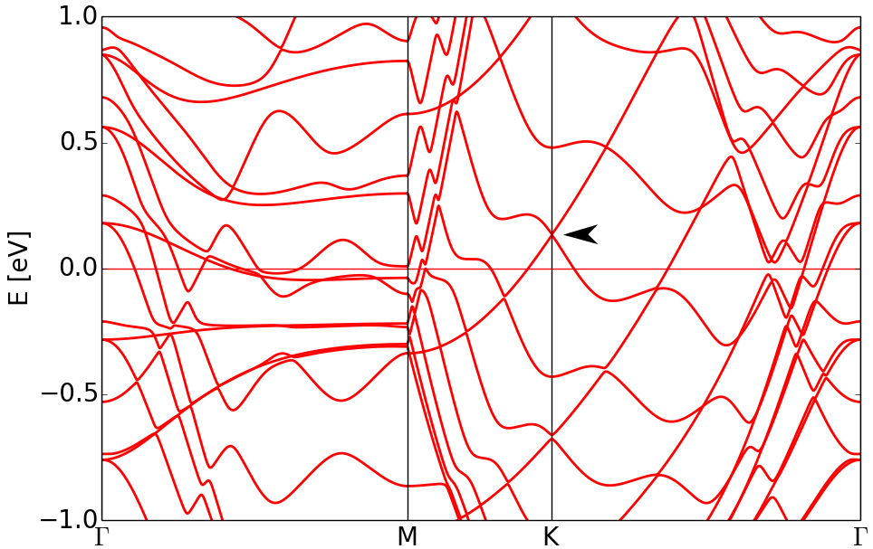
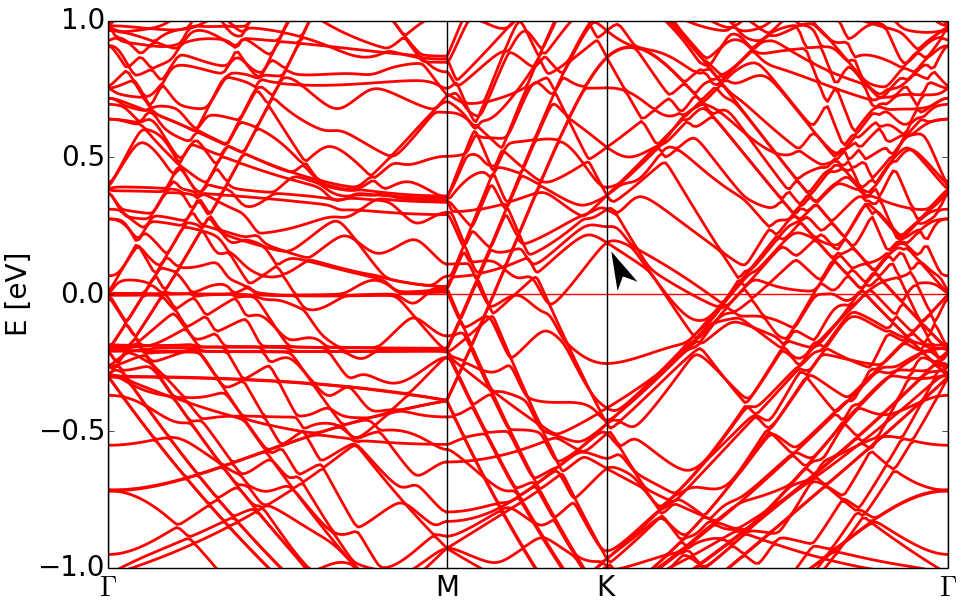
The band structures of the investigated systems reveal a band crossing that resembles the famous Dirac cone located at the symmetry point of the Brillouin zone. The position (energy) of the closest crossing with respect to the Fermi level depends on the CO coverage, and the exact positions are given in Table 2. The band structures of the and systems are shown in Figs. 1 and 2. For the coverage, we observe a clear Dirac cone 0.92 eV above the Fermi energy. In all other cases as the CO coverage reduces, we observe multiple band crossings due to the laterally increasing system size which comprises multiple Cu unit cells. Correspondingly, the band structure becomes more difficult to analyze as the the number of electrons (bands) increases (cf. Figs. 1 and 2). The number of bands is the largest for the 44 coverage, where the CO-CO distances are the largest.
We have performed further band-structure analysis for the 22 surface with the VASP program in order to study the nature of the Kohn-Sham (KS) states close to band-crossing point above the Fermi level. The real space projections of the KS states as a function of wave vector k verify that the symmetry of the KS states changes at the K-point proving that the band crossing is genuine. The states corresponding to the band-crossing point have contribution from both CO and Cu orbitals, but they are not solely localized to the (111) surface. Instead, they have significant weight also deeper in the copper slab. The projected density of states onto atomic orbitals reveals that the CO contribution is still much smaller than Cu contribution for the crossing bands, i.e. the Dirac cone is mostly associated with copper. On the contrary, the contribution of CO increases for the KS states higher in the conduction band, and the next band crossing at 1.12 eV is associated with CO.
We can estimate the Fermi velocities of electrons from the slopes of the bands at the crossing points. The velocities range between m/. As an important factor in the validation of the present model and simulations, our range is of the same order as the value m/s estimated by Gomes et al.Gomes Kenjiro K. et al. (2012) in the experiments for the same system.
| System | Fermi velocity(m/s) | DP pos. (meV) |
|---|---|---|
| 920 | ||
| -110 | ||
| 130 | ||
| -50 | ||
| 190 |
To understand better how CO molecules modify the electronic structure of the Cu(111) surface, we have calculated the charge density difference between (i) the system with both a Cu surface (support) and a CO molecule (adsorbate) and (ii) and the corresponding separated systems:
| (2) |
The surface and the molecule are kept in exactly same positions as in the combined system while computing the separated charge densities. The laterally integrated charge density difference is computed with respect to the -plane, and it is displayed in the neighborhood of the Cu(111) surface for the surface coverage in Fig. 3. In addition, we have computed the charge density difference along the axis of the CO molecule by restricting the integration area within a cylinder of 0.5 Å radius.
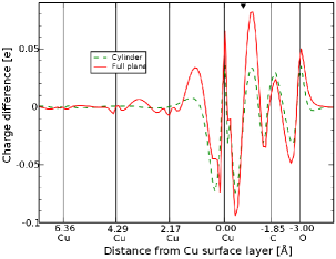
The charge density difference in Fig. 3 shows oscillating features localized around the CO molecule and within the three uppermost Cu layers. The changes are largest at the interface. The chemical interaction between CO and Cu is visible as pronounced oscillations within the contact region (depletion close to Cu, accumulation close to C), but there is no significant charge transfer. The C=O bond has lost some charge while there is accumulation on both C and O atoms. The charge relocation effect is weak around the second and third Cu layer and vanishes deeper in the system.
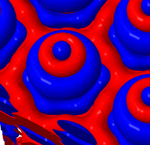
Furthermore, we can investigate the lateral changes in the charge difference by comparing the integration over the full -plane and over a cylinder centered at the CO molecule axis. This analysis reveals a large charge accumulation zone between the CO molecules Å above the top Cu layer, as the cylinder has less accumulation than the whole -plane. In other words, there is less charge accumulation right below the CO molecule (Cu-C contact) than in the surroundings due to a lateral charge-transfer effect. The corresponding electron accumulation zone between the CO molecules has a sixfold symmetry, and it is illustrated in Fig. 4 as a three-dimensional isosurface visualization. The effect is not solely restricted above the Cu surface, and a similar but smaller accumulation pattern can be seen between the Cu layers down to third Cu plane (see Fig. 3). Therefore, we conclude that the adsorption of CO results in a hexagonal charge accumulation pattern in the top layers of the Cu surface, which gives rise to graphene-like electronic properties. The lattice constant of this hexagonal network depends on the CO coverage.
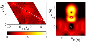
In order to shed more light on the characteristics of the electron density in different locations, we plot the ELF Santis and Resta (2000) in Fig. 5 (colorscale) as cutplane presentations. The ELF gives a measure for electron pairing (localization) by establishing a renormalization of the Fermi hole curvature. Its value varies between zero (no electron localization) and one (electron pairing, covalent bond). Due to employing PAWs in the calculations, the obtained ELF corresponds to the valence or pseudo-ELF, Kohout and Savin (1997) which neglects the electron density of the atomic core. This explains why ELF is nearly zero at atomic sites. However, the pseudo-ELF should give results very similar to the all-electron ELF outside the atomic cores as the valence electrons are delocalized and responsible for chemical bonding.
The covalent character of the C=O bond ELF is visible as a bright yellow color, and the C-Cu contact shows gradual reduction towards metallic bonding. This continuous feature, which is different from the ones observed for a simple charge transfer (ionic bonding) or van der Waals -type physisorption, Akola and Häkkinen (2006) confirms that the interaction between CO and Cu(111) should be described as chemisorption. The ELF analysis (Fig. 5, right) also shows how CO pushes the “metallic” electron density at the surface to the intermediate zone between the adsorbate molecules. The lateral cut-plane presentation (Fig. 5, left) shows further that the locations of these side lobes match with the corners of the hexagonal accumulation zones in Fig. 4, indicating that the corresponding electron density has a delocalized (metallic) character.
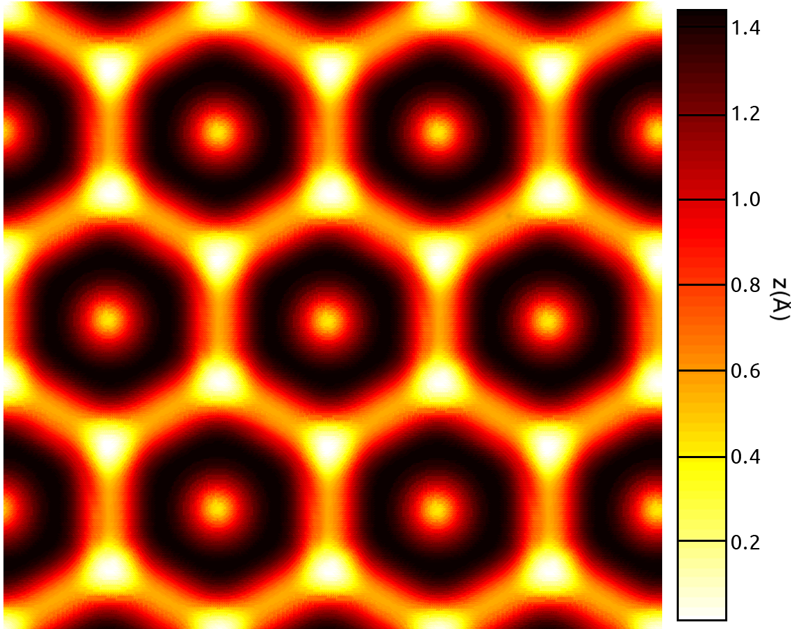
Finally, we have simulated the STM images using the Tersoff-Hamann scheme Tersoff and Hamann (1985) for the surface with 10 mV bias voltage. The result is shown in Fig. 6. The STM image illustrates the hexagonal structure of the surface, i.e., the electrons are expected to primarily move between the CO molecules that form scattering centers similar to those previously modeled in 2D in Ref. Aichinger et al., 2014. The image is very similar to the experimental STM images by Gomes et al.Gomes Kenjiro K. et al. (2012) However, we need to bear in mind that the height difference between CO molecules and intemediate areas is reversed.
To summarize, we have used DFT simulations to investigate a particular form of artificial graphene, carbon monoxide molecules on a copper (111) surface. We observe a Dirac point in the electronic band structure near the Fermi energy at the K-point for different CO coverages. A detailed analysis of the charge density and electron localization show us that the CO adsorption (chemisorption) introduces a lateral charge accumulation in the top layers of Cu(111) with a hexagonal pattern. The associated electron density has a metallic character, and the honeycomb lattice constant is governed by the CO coverage. The theoretical Fermi velocities and STM images are in a reasonable agreement with the experiments, confirming further the validity of the DFT approach. Our first-principles approach can be readily used to study other variants of molecular graphene in the quest of designer Dirac materials.
I Acknowledgements
This work has been supported by the Academy of Finland through its Centre of Excellence Program (Project no. 251748) and through Project No. 126205, European Community’s FP7 through the CRONOS project, Grant Agreement No. 280879, and COST Action CM1204 (XLIC). The computer resources of the Finnish IT Center for Science (CSC) and Finnish Grid Infrastructure (FGI) are acknowledged.
II References
References
- Castro Neto et al. (2009) A. H. Castro Neto, F. Guinea, N. M. R. Peres, K. S. Novoselov, and A. K. Geim, Rev. Mod. Phys. 81, 109 (2009).
- Reich (2013) E. S. Reich, Nature 497, 422 (2013).
- Gomes Kenjiro K. et al. (2012) Gomes Kenjiro K., Mar Warren, Ko Wonhee, Guinea Francisco, and Manoharan Hari C., Nature 483, 306 (2012).
- ”Tarruell et al. (2012) L. ”Tarruell, D. Greif, T. Uehlinger, G. Jotzu, and T. Esslinger, Nature 483, 302 (2012).
- Gibertini et al. (2009) M. Gibertini, A. Singha, V. Pellegrini, M. Polini, G. Vignale, A. Pinczuk, L. N. Pfeiffer, and K. W. West, Phys. Rev. B 79, 241406 (2009).
- Singha et al. (2011) A. Singha, M. Gibertini, B. Karmakar, S. Yuan, M. Polini, G. Vignale, M. I. Katsnelson, A. Pinczuk, L. N. Pfeiffer, K. W. West, and V. Pellegrini, Science 332, 1176 (2011).
- Räsänen et al. (2012) E. Räsänen, C. A. Rozzi, S. Pittalis, and G. Vignale, Phys. Rev. Lett. 108, 246803 (2012).
- Kalesaki et al. (2014) E. Kalesaki, C. Delerue, C. Morais Smith, W. Beugeling, G. Allan, and D. Vanmaekelbergh, Phys. Rev. X 4, 011010 (2014).
- Polini et al. (2013) M. Polini, F. Guinea, M. Lewenstein, H. C. Manoharan, and V. Pellegrini, Nat Nano 8, 625 (2013).
- Sung and Hoffmann (1985) S. S. Sung and R. Hoffmann, Journal of the American Chemical Society 107, 578 (1985).
- Brodén et al. (1976) G. Brodén, T. Rhodin, C. Brucker, R. Benbow, and Z. Hurych, Surface Science 59, 593–611 (1976).
- Hammer et al. (1996) B. Hammer, Y. Morikawa, and J. K. Nørskov, Phys. Rev. Lett. 76, 2141 (1996).
- Stroppa et al. (2007) A. Stroppa, K. Termentzidis, J. Paier, G. Kresse, and J. Hafner, Phys. Rev. B 76, 195440 (2007).
- Gajdoš and Hafner (2005) M. Gajdoš and J. Hafner, Surface Science 590, 117 (2005).
- Aichinger et al. (2014) M. Aichinger, S. Janecek, I. Kylänpää, and E. Räsänen, Phys. Rev. B 89, 235433 (2014).
- Blum et al. (2009) V. Blum, R. Gehrke, F. Hanke, P. Havu, V. Havu, X. Ren, K. Reuter, and M. Scheffler, Computer Physics Communications 180, 2175 (2009).
- Perdew et al. (1996) J. P. Perdew, K. Burke, and M. Ernzerhof, Phys. Rev. Lett. 77, 3865 (1996).
- Kresse and Furthmüller (1996) G. Kresse and J. Furthmüller, Phys. Rev. B 54, 11169 (1996).
- Kresse and Joubert (1999) G. Kresse and D. Joubert, Phys. Rev. B 59, 1758 (1999).
- Blöchl (1994) P. E. Blöchl, Phys. Rev. B 50, 17953 (1994).
- Straumanis and Yu (1969) M. E. Straumanis and L. S. Yu, Acta Crystallographica Section A 25, 676 (1969).
- Hirshfeld (1977) F. Hirshfeld, Theoretica chimica acta 44, 129 (1977).
- Santis and Resta (2000) L. D. Santis and R. Resta, Surface Science 450, 126–132 (2000).
- Kohout and Savin (1997) M. Kohout and A. Savin, Journal of Computational Chemistry 18, 1431 (1997).
- Akola and Häkkinen (2006) J. Akola and H. Häkkinen, Phys. Rev. B 74, 165404 (2006).
- Tersoff and Hamann (1985) J. Tersoff and D. R. Hamann, Phys. Rev. B 31, 805 (1985).