Excitonic condensation in spatially separated one-dimensional systems
Abstract
We show theoretically that excitons can form from spatially separated one-dimensional ground state populations of electrons and holes, and that the resulting excitons can form a quasicondensate. We describe a mean-field Bardeen-Cooper-Schrieffer theory in the low carrier density regime and then focus on the core-shell nanowire giving estimates of the size of the excitonic gap for InAs/GaSb wires and as a function of all the experimentally relevant parameters. We find that optimal conditions for pairing include small overlap of the electron and hole bands, large effective mass of the carriers, and low dielectric constant of the surrounding media. Therefore, one-dimensional systems provide an attractive platform for the experimental detection of excitonic quasicondensation in zero magnetic field.
pacs:
71.35.-y, 73.21.Hb, 67.85.JkExcitonic condensation is the formation of a macroscopic condensed state of bosons consisting of paired electrons and holes. Lozovik and Yudson (1976) The quasiparticles which comprise this boson may come either from optically pumped (and hence transient) states, or from spatially separated ground state populations which are stable for, in principle, infinite time. In addition to being a highly interesting physical phenomenon, the excitonic condensate may have important technological applications such as in dispersionless switching devices,Banerjee et al. (2009) an analogue-to-digital converter,Dolcini et al. (2010) and for the design of topologically protected qubits. Peotta et al. (2011) Spatially separated exciton condensates have a long history of consideration in two dimensions (2D), where electron-hole bilayers made first from semiconductor heterostructures,Lozovik and Yudson (1976) and later from two graphene layers Zhang and Joglekar (2008); Min et al. (2008) were proposed as systems where this phenomenon could be observed. However, the only clear experimental evidence for such a state has been seen in a strong magnetic field,Eisenstein and MacDonald (2004); Nandi et al. (2012) and despite much effort, the excitonic condensate has not been observed in zero field. Pillarisetty et al. (2002); Seamons et al. (2009); Kim et al. (2011); Gorbachev et al. (2012); Gamucci et al. (2014) Theoretical estimates indicate that monolayer graphene systems with conical band structures are probably too weakly interacting for the condensate to manifest at zero field, Sodemann, Pesin, and MacDonald (2012); Lozovik, Ogarkov, and Sokolik (2012) but that multilayer graphene systems may be an attractive platform.Zhang and Rossi (2013); Perali, Neilson, and Hamilton (2013); Zarenia et al. (2014)
Such excitonic condensation formally cannot exist in one dimension (1D) in the true sense of having long-range order, but correlations between excitons may exist at finite length scales and are characterised by a power law decay. Cazalilla et al. (2011); Guan, Batchelor, and Lee (2013) We propose that this ‘quasicondensation’ may be supported in various experimentally relevant condensed matter systems 111Additionally, constructing quasi-1D systems of superconducting metals has been shown to enhance the critical temperature with respect to the bulk system. See A. Bianconi, A. Valletta, A. Perali, and N. L. Saini, Physica C: Supercond. 296, 269 (1998), A. A. Shanenko, M. D. Croitoru, M. Zgirski, F. M. Peeters, and K. Arutyunov, Phys. Rev. B 74, 052502 (2006) and references therein. including stacked graphene nanoribbons, Brey and Fertig (2006) in nanowires or carbon nanotubes arranged side-by-side,Werman and Berg (2014) in a core-shell nanowire (CSN), Ganjipour et al. (2012) in nanowires constructed from adjacent electron-doped and hole-doped GaAs quantum wells, or in nanowires patterned from a InAs/GaSb double quantum well. These setups are illustrated schematically in Fig. 1. In all candidate systems, the important experimental prerequisites are that the electron and hole populations are simultaneously present in the ground state and separated by a finite distance . If transport measurements are employed to detect the condensate, then independent contacting of the two layers is essential to allow either Coulomb drag measurements,Su and MacDonald (2008) or measurement of the tunneling current between the two layers.Eisenstein and MacDonald (2004) In the case of stacked graphene, this has been demonstrated many times in 2D since the two layers can be gated from opposite sides Gorbachev et al. (2012) and contacting the two layers is also straightforward. The growth process of CSNs will also allow this, since it is possible to grow the shell around only some length of the core and hence leave both materials exposed for independent contacting. Alternatively, optical probes could be used which do not require contacts.

In this Letter, we present the mean-field BCS theory that is applicable for all spatially separated 1D electron and hole systems in the limit of low carrier density. We then give numerical results which illustrate the behavior of a CSN as it depends on the material parameters. Finally, we discuss some specific practical details of CSN systems, and how excitonic quasicondensation would differ in the other possible setups. Previously, excitonic condensation has been considered in 1D in the context of the high density limit of optical excitations, Nagaosa and Ogawa (1993) BCS theory was applied to cold fermionic gases generally using a short-range interaction,Schlottmann (1994); Bruun et al. (1999); Bedaque, Caldas, and Rupak (2003); Tokatly (2004); Ying et al. (2008) in carbon nanotubes,Bondarev and Meliksetyan (2014) and in a nonequilibrium context.Zachmann et al. (2013) However, spatially separated solid state systems have only been investigated for excitonic quasicondensation once,Werman and Berg (2014) where the language of bosonization was used and only qualitative predictions for the interwire tunneling current were given.
The general theory consists of a Hamiltonian where contains the single particle terms and is the interwire interaction. We assume that both the electron and hole regions contain one nondegenerate band and allow for independent chemical potentials in each region. 222For a realistic spin-degenerate material this one band approximation can be realised using the Zeeman splitting associated with a magnetic field (since Landau levels will not occur in 1D) or with a ferromagnetic substrate. The annililation operator for an electron in one of these bands is denoted where indicates the band, and is the momentum. Since we enforce one band to be electron-like and the other to be hole-like we introduce the following notation: is the annihilation of an electron in layer 1, and is the annihilation of a hole in layer 2. The single particle part of the Hamiltonian is
with and . This Hamiltonian does not include any interwire tunneling but we qualitatively discuss its effect below. Also, in principle a realistic 1D system will contain many subbands, but in the low density limit we assume that only the first subband plays an active role in the excitonic pairing.
The interwire interaction between the electrons and holes is derived within mean-field BCS theory. Liu, Hu, and Drummond (2007); Parish et al. (2007); Edge and Cooper (2009) This is valid at low temperature (when is much less than the mean-field critical temperature ) and when the interlayer interaction is sufficiently strong, Werman and Berg (2014) corresponding to the limit where separation of the two carrier species is less than the average separation of carriers within each wire given by the inverse of the carrier density, so that the instability towards exciton formation dominates over the tendency to form a Luttinger liquid state within each wire. For this to be the case, we require (where is the Fermi wave vector), and for physically realistic parameters and a quadratic band, this condition is satisfied for . The resulting interaction Hamiltonian is where is defined as the self-consistent solution of the equation
| (1) |
where are the occupation factors for the bands at wave vector . The quantity is the Fourier transform of the interwire interaction and is given by
where is the modified Bessel function of the second kind 333This Bessel function diverges as , so we impose a minimum cutoff . We have tested that the precise value of this cutoff does not impact the numerical results. and in SI units. The minus sign appears because each 1D system contains carriers of opposite charge so that their Coulomb interaction is attractive. In principle, a form factor can also appear in Eq. (1), but this typically produces only a small quantitative change in the gap function. Also, if the mismatch in dielectric constants between the core and shell region is large, this may contribute a substantial renormalisation of the excition binding energy. Slachmuylders et al. (2006) This Hamiltonian is diagonalized using a Bogolyuobov transformation which yields two excitonic bands with dispersion
This indicates that, for finite , a gap opens in the single particle spectrum near the points where the two single particle bands cross, and the magnitude of this gap is exactly evaluated at the wave vector of the crossing point. Therefore, this value represents the turning point of each of the excitonic bands and hence the overall gap of these bands from the excitonic level. Hence, it is called the ‘excitonic gap’, and label it by .
However, to give a concrete example and experimentally relevant predictions, we make our theory specific to the CSN. The CSN is a particularly interesting case since it has recently been demonstrated that certain combinations of core and shell materials allow for simultaneous populations of holes in the core region and electrons in the shell region, minimal hybridization between them, and ambipolar transport characteristics. Ganjipour et al. (2012) Here, it is reasonable to approximate the low energy band structure in a quadratic form Pistol and Pryor (2008); Kishore, Partoens, and Peeters (2012) parameterized by a band offset and an effective mass such that
One important combination of materials is a CSN with a core (hole) region of GaSb and a shell (electron) region of InAs. Using parameters from Ref. Pistol and Pryor, 2008, we take band extrema of and , and effective masses of and . This pair of materials fulfills the general requirements for the excitons to exist: they have bands that overlap with opposite sign of the effective mass. We assume a dielectric constant of in both materials so that the dielectric mismatch is zero and there is no renormalisation of the exciton binding energy.
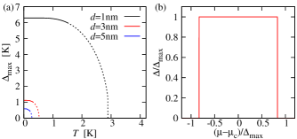
The pairing happens most strongly when the chemical potential is placed at the point where the two bands cross, given by . Figure 2(a) shows the predicted maximum of the gap function for a InAs/GaSb CSN as function of temperature for various inter-wire spacings and . We stress that the mean-field BCS will not give a quantitatively accurate estimate of the critical temperature () so the higher-temperature part is shown as a dotted line to emphasize this. The estimated gap size is of the order of one milli-electron volt at , so that the associated is of the order of a few Kelvin, and is strongly dependent on the spacing between the electron and hole populations. Figure 2(b) shows how behaves as a function of the chemical potential at . As moves away from the band crossing at , the gap stays unchanged until a certain point where it collapses to zero immediately. This is caused by the minimum of one of the excitonic bands becoming negative and allowing for gapless excitations at the Fermi energy which are energetically favorable to the exciton state, in close analogy to the Clogston-Chandrasekhar limit for a superconductor in a magnetic field. The value of the chemical potential for which this happens at , (which we label ), is
| (2) |
For the parameters appropriate to the InAs/GaSb CSN we find . The coefficient of in the second term is peaked when indicating that the exciton is the most robust against shifts in the chemical potential when the band masses have equal magnitude.
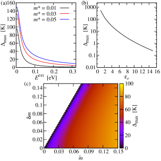
In principle, the choice of material for the core and shell regions could be made so as to optimize the excitonic gap. Therefore, we analyze at as a function of the band parameters and dielectric constant. Figure 3(a) shows as a function of the overlap of the two bands such that for three different values of the effective masses defined such that . We fix all other parameters. This indicates that the pairing is strongest when is close to the band extrema so that the Fermi surface is small and the carrier density is low. Figure 3(c) shows as a function of the band masses. Here, we arrange the notation such that and while fixing the criteria that and . The unfilled region in the upper-left part of the plot is the parameter space where these criteria cannot be satisfied. Looking first along the axis, we see that increases with the band masses. This, taken together with the observations from Fig. 3(a) indicate that flatter bands (and hence a higher density of states) increases the excitonic gap. Allowing to be finite shows that imbalance in the two effective masses is detrimental to the excitonic pairing, although this effect diminishes as increases. Figure 3(b) shows that the dielectric constant of the medium is also a crucial parameter. We find that suppression of the excitonic gap with increasing is slightly sub-exponential.
Since we focus on the CSN system where there is no spacer layer between the electron and hole regions, we have to take the possible direct tunneling of carriers between the two bands, and the resulting hybridization of the single particle bands into account. The hybridization of bands in the context of 2D excitonic condensation has been analyzed previously Sodemann, Pesin, and MacDonald (2012); Efimkin, Lozovik, and Sokolik (2012) where it was found that a small hybridization was beneficial to the formation of a gap at the Fermi energy, since it adds a single particle contribution to the channel. In fact, some finite amount of interwire hybridization is essential for the operation of the BiSFET device Banerjee et al. (2009) and hence the CSN provides an excellent platform for its implementation.
The situation with stacked graphene nanoribbons will be qualitatively similar to that discussed for CSNs. For armchair nanoribbons, the dispersion associated with the single particle bands will change to where is the Fermi velocity of the Dirac cone of the graphene, the sign reflects the conduction or valence band, and is the extremum of the lowest subband and is set by the ribbon geometry.Brey and Fertig (2006) A form factor resulting from the sublattice structure of the underlying graphene also has to be added to Eq. (1) which will manifest as a small quantitative reduction in the gap size. The chemical potential of the two layers may be set independently by gating the stacked ribbons from above and below, but the most advantageous situation will occur when the Fermi points in the two layers are at the same wave vector.
For graphene systems, it is well known that the crystal lattice structure is of remarkably high quality, and that the dominant form of disorder is charged impurities trapped in the environment of the flake. In 2D, the effect of the fluctuations in the local charge density resulting from these impurities has been shown to be highly detrimental to the stability of the condensate.Abergel, Sensarma, and Das Sarma (2012); Abergel et al. (2013) This will be no different for stacked graphene nanoribbons and so a result analogous to that in Eq. (2) will characterise the stability of the 1D quasicondensate against local fluctuations in the chemical potential. For III-V semiconductor systems such as the CSNs, growth-related disorder such as width fluctuations will be important. However, these will also generate a local shift in the chemical potential, and so as long as is not exceeded locally, the exciton formation will be unaffected.
In conclusion, we have demonstated that excitonic pairing and the resulting quasicondensation has a realistic chance of being observed in 1D systems. In particular, CSNs provide a likely platform for its observation, with an excitonic gap of the order of Kelvin for thin InAs/GaSb wires. This gap size may be substantially increased by choosing materials with higher effective mass, decreased band overlap, and reduced dielectric constant. Throughout, we assume that the interaction between wires is stronger than the interaction within each wire, so that the Luttinger liquid effects are neglected. This is a strong approximation, but current experimental transport data on CSNs show no evidence of Luttinger liquid effects. Ganjipour et al. (2012) In particular, metallic InAs nanowires show improved conductance as the temperature is lowered, and there is no evidence of suppression of tunneling into core-shell nanowires at low temperature.Thelander (2014)
We wish to thank Martin Leijnse, Claes Thelander, Bahram Ganjipour, Adrian Kantian, and Alexander Balatsky for helpful discussions. This work was supported by ERC DM-321031 and by Nordita.
References
- Lozovik and Yudson (1976) Y. E. Lozovik and V. Yudson, JETP 44, 389 (1976).
- Banerjee et al. (2009) S. Banerjee, L. Register, E. Tutuc, D. Reddy, and A. MacDonald, IEEE Electron Device Lett. 30, 158 (2009).
- Dolcini et al. (2010) F. Dolcini, D. Rainis, F. Taddei, M. Polini, R. Fazio, and A. H. MacDonald, Phys. Rev. Lett. 104, 027004 (2010).
- Peotta et al. (2011) S. Peotta, M. Gibertini, F. Dolcini, F. Taddei, M. Polini, L. B. Ioffe, R. Fazio, and A. H. MacDonald, Phys. Rev. B 84, 184528 (2011).
- Zhang and Joglekar (2008) C.-H. Zhang and Y. Joglekar, Phys. Rev. B 77, 233405 (2008).
- Min et al. (2008) H. Min, R. Bistritzer, J.-J. Su, and A. MacDonald, Phys. Rev. B 78, 121401 (2008).
- Eisenstein and MacDonald (2004) J. P. Eisenstein and A. H. MacDonald, Nature 432, 691 (2004).
- Nandi et al. (2012) D. Nandi, A. D. K. Finck, J. P. Eisenstein, L. N. Pfeiffer, and K. W. West, Nature 488, 481 (2012).
- Pillarisetty et al. (2002) R. Pillarisetty, H. Noh, D. Tsui, E. De Poortere, E. Tutuc, and M. Shayegan, Phys. Rev. Lett. 89, 016805 (2002).
- Seamons et al. (2009) J. A. Seamons, C. P. Morath, J. L. Reno, and M. P. Lilly, Phys. Rev. Lett. 102, 026804 (2009).
- Kim et al. (2011) S. Kim, I. Jo, J. Nah, Z. Yao, S. K. Banerjee, and E. Tutuc, Phys. Rev. B 83, 161401 (2011).
- Gorbachev et al. (2012) R. V. Gorbachev, A. K. Geim, M. I. Katsnelson, K. S. Novoselov, T. Tudorovskiy, I. V. Grigorieva, A. H. MacDonald, S. V. Morozov, K. Watanabe, T. Taniguchi, and L. A. Ponomarenko, Nature Phys. 8, 896 (2012).
- Gamucci et al. (2014) A. Gamucci, D. Spirito, M. Carrega, B. Karmakar, A. Lombardo, M. Bruna, L. N. Pfeiffer, K. W. West, A. C. Ferrari, M. Polini, and et al., Nature Commun. 5, 5824 (2014).
- Sodemann, Pesin, and MacDonald (2012) I. Sodemann, D. A. Pesin, and A. H. MacDonald, Phys. Rev. B 85, 195136 (2012).
- Lozovik, Ogarkov, and Sokolik (2012) Y. E. Lozovik, S. L. Ogarkov, and A. A. Sokolik, Phys. Rev. B 86, 045429 (2012).
- Zhang and Rossi (2013) J. Zhang and E. Rossi, Phys. Rev. Lett. 111, 086804 (2013).
- Perali, Neilson, and Hamilton (2013) A. Perali, D. Neilson, and A. Hamilton, Phys. Rev. Lett. 110, 146803 (2013).
- Zarenia et al. (2014) M. Zarenia, A. Perali, D. Neilson, and F. M. Peeters, Sci. Rep. 4, 7319 (2014).
- Cazalilla et al. (2011) M. A. Cazalilla, R. Citro, T. Giamarchi, E. Orignac, and M. Rigol, Rev. Mod. Phys. 83, 1405 (2011).
- Guan, Batchelor, and Lee (2013) X.-W. Guan, M. T. Batchelor, and C. Lee, Rev. Mod. Phys. 85, 1633 (2013).
- Note (1) Additionally, constructing quasi-1D systems of superconducting metals has been shown to enhance the critical temperature with respect to the bulk system. See A. Bianconi, A. Valletta, A. Perali, and N. L. Saini, Physica C: Supercond. 296, 269 (1998), A. A. Shanenko, M. D. Croitoru, M. Zgirski, F. M. Peeters, and K. Arutyunov, Phys. Rev. B 74, 052502 (2006) and references therein.
- Brey and Fertig (2006) L. Brey and H. Fertig, Phys. Rev. B 73, 235411 (2006).
- Werman and Berg (2014) Y. Werman and E. Berg, ArXiv e-prints (2014), arXiv:1408.2718 [cond-mat.mes-hall] .
- Ganjipour et al. (2012) B. Ganjipour, M. Ek, B. Mattias Borg, K. A. Dick, M.-E. Pistol, L.-E. Wernersson, and C. Thelander, Appl. Phys. Lett. 101, 103501 (2012).
- Su and MacDonald (2008) J.-J. Su and A. H. MacDonald, Nature Phys. 4, 799 (2008).
- Nagaosa and Ogawa (1993) N. Nagaosa and T. Ogawa, Solid State Commun. 88, 295 (1993).
- Schlottmann (1994) P. Schlottmann, J. Phys.: Condens. Matter 6, 3719 (1994).
- Bruun et al. (1999) G. Bruun, Y. Castin, R. Dum, and K. Burnett, Euro. Phys. J. D 7, 433 (1999).
- Bedaque, Caldas, and Rupak (2003) P. Bedaque, H. Caldas, and G. Rupak, Phys. Rev. Lett. 91, 247002 (2003).
- Tokatly (2004) I. V. Tokatly, Phys. Rev. Lett. 93, 090405 (2004).
- Ying et al. (2008) Z.-J. Ying, M. Cuoco, C. Noce, and H.-Q. Zhou, Phys. Rev. Lett. 100, 140406 (2008).
- Bondarev and Meliksetyan (2014) I. V. Bondarev and A. V. Meliksetyan, Phys. Rev. B 89, 045414 (2014).
- Zachmann et al. (2013) M. Zachmann, M. D. Croitoru, A. Vagov, V. M. Axt, T. Papenkort, and T. Kuhn, New J. Phys. 15, 055016 (2013).
- Note (2) For a realistic spin-degenerate material this one band approximation can be realised using the Zeeman splitting associated with a magnetic field (since Landau levels will not occur in 1D) or with a ferromagnetic substrate.
- Liu, Hu, and Drummond (2007) X.-J. Liu, H. Hu, and P. D. Drummond, Phys. Rev. A 76, 043605 (2007).
- Parish et al. (2007) M. M. Parish, S. K. Baur, E. J. Mueller, and D. A. Huse, Phys. Rev. Lett. 99, 250403 (2007).
- Edge and Cooper (2009) J. M. Edge and N. R. Cooper, Phys. Rev. Lett. 103, 065301 (2009).
- Note (3) This Bessel function diverges as , so we impose a minimum cutoff . We have tested that the precise value of this cutoff does not impact the numerical results.
- Slachmuylders et al. (2006) A. F. Slachmuylders, B. Partoens, W. Magnus, and F. M. Peeters, Phys. Rev. B 74, 235321 (2006).
- Pistol and Pryor (2008) M.-E. Pistol and C. Pryor, Phys. Rev. B 78, 115319 (2008).
- Kishore, Partoens, and Peeters (2012) V. V. R. Kishore, B. Partoens, and F. M. Peeters, Phys. Rev. B 86, 165439 (2012).
- Efimkin, Lozovik, and Sokolik (2012) D. K. Efimkin, Y. E. Lozovik, and A. A. Sokolik, Phys. Rev. B 86, 115436 (2012).
- Abergel, Sensarma, and Das Sarma (2012) D. S. L. Abergel, R. Sensarma, and S. Das Sarma, Phys. Rev. B 86, 161412 (2012).
- Abergel et al. (2013) D. S. L. Abergel, M. Rodriguez-Vega, E. Rossi, and S. Das Sarma, Phys. Rev. B 88, 235402 (2013).
- Thelander (2014) C. Thelander, private communication (2014).