Chiral tunneling of topological states: towards the efficient generation of spin current using spin-momentum locking
Abstract
We show that the interplay between chiral tunneling and spin-momentum locking of helical surface states leads to spin amplification and filtering in a 3D Topological Insulator (TI). Chiral tunneling across a TI junction allows normally incident electrons to transmit, while the rest are reflected with their spins flipped due to spin-momentum locking. The net result is that the spin current is enhanced while the dissipative charge current is simultaneously suppressed, leading to an extremely large, gate tunable spin to charge current ratio (20) at the reflected end. At the transmitted end, the ratio stays close to one and the electrons are completely spin polarized.
Since their theoretical prediction and experimental verification in quantum wells and bulk crystals, Topological Insulators have been of great interest in condensed matter physics, even prompting their classification as a new state of matterQi and Zhang (2011). The large spin orbit coupling in a TI leads to an inverted band separated by a bulk bandgap. Symmetry considerations dictate that setting such a TI against a normal insulator (including vacuum) forces a band crossing at their interface, leading to gapless edge (for 2D) and surface (for 3D) states protected by time reversal symmetry. At low energies, the TI surface Hamiltonian Qi and Zhang (2011) resembles the graphene Hamiltonian except that the Pauli matrices in TI represent real-spins instead of pseudo-spins in graphene. This suggests that the chiral tunneling (the angle dependent transmission) in a graphene junctionCheianov and Fal’ko (2006); Young and Kim (2009); Sajjad et al. (2012); Sajjad and Ghosh (2013) is expected to appear in a TI pn junction (TIPNJ) as well. Although TIPNJs have been studied recentlyWu et al. (2011); Takahashi and Murakami (2011); Wang et al. (2012), the implication of chiral tunneling combined with spin-momentum locking in spintronics has received little attention.
The energy dissipation of a spintronic device strongly depends on the efficiency of spin current generation. The efficiency is measured by the spin-charge current gain , where and are the non-equilibrium spin and charge currents respectively. Increasing reduces the energy dissipation quadratically. The gain for a regular magnetic tunnel junction is less than 1Datta et al. (2015). The discovery of Giant Spin Hall Effect (GSHE)Liu et al. (2012) shows a way to achieve by augmenting the spin Hall angle with an additional geometrical gainDatta et al. (2012). The intrinsic gain for various metals and metal alloys has been found to vary between 0.07-0.3Mosendz et al. (2010); Liu et al. (2012, 2011). Recently, Bi2Se3 based TI has been reported to have ‘spin torque ratio’ (a quantity closely related to ) of 2-3.5Mellnik et al. (2014) and has been shown to switch a soft ferromagnet at low temperatureFan et al. (2014). An oscillatory spin polarization has also been predicted in TI using a step potentialGao et al. (2011).
In this letter, we show that the interplay between the chiral tunneling and spin momentum locking in TIPNJ shown in Fig. 1 leads to an extremely large, electrically tunable spin-charge current gain even without utilizing any geometric gain. The chiral tunneling in TIPNJ only allows electrons with very small incident angle to pass through and all other electrons are reflected back to the source in the same way as graphene. As a result, charge current going through the junction decreases. Due to spin-momentum locking, the injected electrons have down spin but the reflected electrons have up spin, which enhances the spin current at the source contact. These result in a gate tunable, extraordinarily large spin-charge current gain. We show below that in a split-gate, symmetrically doped TIPNJ, the spin-charge current gain is,
| (1) |
at the source contact for small drain bias. Here, is the reflection probability averaged over all modes, is the built in potential of the TIPNJ and is the split between the gates. For large bias, Eq. 1 can be approximated as . In a typical TIPNJ with nm, V and m/s, at source is 30 for small bias and 20 for large bias. At drain, remains close to 1. We also show below that the region is highly spin polarized since only the small angle modes (with spin-) exist there. The large in a TIPNJ does not require any geometrical gain and can potentially be larger than the net gain in GSHE systems like -Ta and WManipatruni et al. (2014) that rely on the additional geometrical gain. In addition, it is gate tunable, meaning that we can turn its value continuously from 1.5 to 20. The directions of spin and charge are parallel in TIPNJ, as opposed to the transverse flow in GSHE.
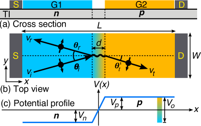
The cross section and the top view of the model TIPNJ device are shown in Fig. 1a and 1b respectively. The 3D TI is assumed to be Bi2Se3 which has the largest bulk bandgap of meV. The source (S) and the drain (D) contacts are placed on the top surface of the TI slab. We assume that the electron conduction happens only on the top surface. This is a good approximation since the device is operated within the bulk bandgap to minimize the bulk conduction and we numerically verified that only a small part of the total current goes through the side walls which was also seen in experimentLee et al. (2014). The and regions are electrically doped using two external gates G1 and G2 separated by the split distance . Such gate controlled doping of TI surface states has been demonstrated experimentally for Bi2Se3Chen et al. (2010). The device has a built-in potential distributed between the and regions as shown in Fig. 1c assuming a linear potential profile inside the split region. Electrons are injected from source and collected at drain by a bias voltage .
Although an equilibrium spin current exists on the TI surface, it has no consequences for the measurable spin currentBurkov and Hawthorn (2010); Tserkovnyak and Loss (2012). Therefore, we only considered the non-equilibrium spin current. There has been a lot of discussions on the equilibrium spin current in the literatureRashba (2003); Tokatly (2008); Sonin (2007); MAHFOUZI and NIKOLIĆ (2013). In this article, we choose a biasing scheme that defines the equilibrium state. We connect the drain contact to the ground and reference the gates with respect to the ground so that and where and are the chemical potentials of the drain and the source contacts respectively. The equilibrium current, is then defined by and . The non-equilibrium spin current is obtained by subtracting from the total spin current calculated for nonzero bias ( and ). A detailed description of this method is discussed in the Supplement.
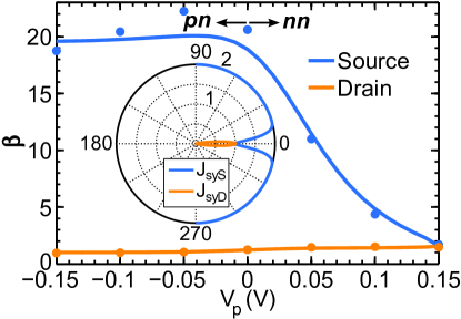
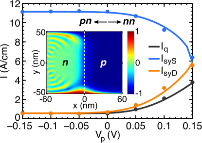
The spin current, the charge current and the spin to charge current ratio are shown in Figs. 2-3 as functions of gate bias of the region. The solid lines were calculated using Eqs. 2-4 and S3 evaluated at the source and drain contacts. The discrete points were calculated using the non-equilibrium Green’s function (NEGF) formalism and the discretized k.p Hamiltonian which captures the effects of edge reflections. Both analytical and numerical simulations were done for a device with length nm, width nm, split length nm, drain bias V, gate voltage V at room temperature. When the gate voltage of region V, the channel is a perfect type with uniform potential profile. Thus, all the modes are allowed to transmit from the source to the drain and there is no reflection. Hence, the charge current is maximum, spin current at the source and drain are equal and as shown in Fig. 3. When the gate voltage is decreased to -0.15 V, the potential profile is no longer uniform, the channel becomes a junction and most of the electrons are reflected back from the junction and therefore, charge current is reduced. Since the incident and reflected waves have opposite spins, the reflected waves enhances the spin current at the source end and becomes large at the source contact. In the drain contact, however, only the transmitted electrons are collected and remains close to 1. Thus, changes from to at source contact and remains close to at the drain when the device is driven from the to the regime. The agreement between the numerical and the analytical results shown in Figs. 2 and 3 indicates that the physics described here is robust against the edge reflection at finite drain bias and room temperature.
Let us now derive Eq. 1 and analyze the underlying physics. We start with the effective Hamiltonian for 3D TI surface states and follow the similar procedure as described in Ref.Sun and Xie (2005) to obtain the continuity equation for spin, . Here, is a rank 2 tensor describing the translational motion of spin and is a vector describing the rate of change of spin density due to spin precession at location and time . The quantity is also referred to as spin torqueSun and Xie (2005). Among nine elements of , only and are nonzero for TI. The current density operator describes spin current carried by spin- along direction etc. Inside the gate regions where there is no scattering, the angular term is zero and the spin current is conserved. However, at the junction interface, electrons are reflected which is accompanied by a change in the spin angular momentum. As a result, inside the junction interface, and the spin current is not conserved (see the Supplement). At steady state, and hence, for the two terminal device shown in Fig. 1, the difference between the spin currents at the source and the drain terminal is the spin torque generated by the TIPNJ. Similarly, we obtain the charge current density operators and where describes the motion of electrons moving along the direction. For the TIPNJ, since there is no net charge or spin transfer in direction, and .
The wavefunction of an electron in the side () of the TIPNJ shown in Fig. 1 can be expressed as where is the incident wave, is the reflected wave and is the reflection coefficient. The general form of spin-momentum locked incident wave with incident angle and energy is where is the area of the device, is the wavevector with magnitude and direction and . Similarly, the reflected wave is given by where and . In the side (), only the transmitted wave exist. Hence, the wave function of electron is expressed as with where wavevector , is the transmission angle, is the transmission coefficient and . Since the potential along is uniform, the component of wavevector must be conserved throughout the device. Thus, we recover Snell’s law for TI surface state: . It follows from Snell’s law and the opposite helicity of conduction and valence bands of TI surface states that the transmission angle for and for where . For electrons with , becomes complex and the electrons are reflected back to the source.
Inside the junction interface (), the wavevector varies in accordance with . For electrons with , the component of becomes imaginary, the wavefunctions become evanescent and the electrons are reflected back. Considering the exponential decay inside the interface and matching the wavefunction across an abrupt junction, the transmission coefficient can be written as where and is the imaginary part of .
Now, let us consider an electron injected from the source at angle and energy is transmitted from to and collected at drain. The probability current density for the transmitted electron is given by which leads to the general expression for the charge current density
| (2) |
where , and . Similarly, the probability current density for the incident wave is . Hence, the transmission probability is given by , which is the general form of transmission probability in graphene junction as presented in Refs. Sajjad et al. (2012); Cheianov and Fal’ko (2006) and valid for all energies in , and regime. Similarly, the spin current density at drain is
| (3) |
where the negative sign indicates that the spin current is carried by the down spin. The spin current at source has two components: (1) the incident current and the reflected current Therefore, the total spin current density is,
| (4) |
where . Eqs. 2-4 are valid for all energies in , and regimes. The total current is the sum of contributions from all electrons with positive group velocity along , weighted by the Fermi functions and integrated over all energies as given by Eq. S3. Unlike the incident and reflected components of charge currents, and have the same sign. This is because when a spin-up electron is reflected from the junction interface, its spin is flipped due to the spin-momentum locking. Now, a spin-down electron going to the left has the same spin current as a spin-up electron going to the right. Hence, the spin currents due to the injected and the reflected electron add up enhancing the source spin current.
For symmetric junction, within the barrier (), the transmission coefficient is dominated by the exponential term and becomes . Hence, is nonzero for electrons with very small incident angle (). For these electrons, , and . Therefore, the transmission probability becomes,
| (5) |
which has the same form as the transmission probability in graphene junctionSajjad et al. (2012); Cheianov and Fal’ko (2006). The charge current density in symmetric junction is then,
| (6) |
and spin current densities at drain and source are
| (7) |
where and signs are for and respectively, and is the reflection probability. Now, the spin-charge current gain can be expressed as in the low bias limit. For symmetric junction, at the source contact reduces to the first expression in Eq. 1 where is the average reflection probability. When the Fermi energy is at the middle of the barrier, and is given by the second term of Eq. 1.
Eq. 5 clearly shows that is nonzero only for electrons with very small . Hence, only these electrons are allowed to transmit. For all other modes, the reflection probability and those electrons are reflected back from the junction interface to the source. Thus, only few modes with small contribute to and , whereas all other modes contribute to as shown in the inset of Fig. 3. This is also consistent with the spin polarization of TIPNJ shown in the inset of Fig. 2 calculated using NEGF with negligible injection from the drain. In the side, only the transmitted waves exist and the spins of these electrons are aligned to due to the spin-momentum locking. Therefore, the side is highly spin polarized as illustrated by blue. On the other hand, in the side, both the incident and the reflected waves exist with spins aligned to all the directions in plane leading to the unpolarized region indicated by green. This is completely different from the uniform or device where the spin polarization is throughout the channelYazyev et al. (2010); Hong et al. (2012). Thus, the spin polarization shown in Fig. 2 is a key signature of spin filtering and amplification effect in TIPNJ, which can be measured by spin resolved scanning tunneling microscopy.
One way to measure is to pass the spin current through a ferromagnetic metal (FM) by using the FM as the source contact of TIPNJ. The magnetization of the FM needs to be in-plane so that it does not change the TI bandstructure. The spin current going through the FM will exert torque on the FM which can be measured indirectly using spin torque ferromagnetic resonance techniqueMellnik et al. (2014) or directly by switching the magnetization (along ) of soft ferromagnets such as (CrxBiySb1-x-y)2Te3 at low temperatureFan et al. (2014). Once the magnetization of the FM is switched from to , the current injection will stop (since spin up states cannot move towards right) and the system will reach the stable state.
In summary, we have shown that the chiral tunneling of helical states leads to an large spin-charge current gain due to the simultaneous amplification of spin current and suppression of charge current in a 3D TIPNJ. The chiral tunneling allows only the near normal incident electrons to transmit, suppressing the charge current significantly. The rest of the electrons are reflected and their spins are flipped due to the spin-momentum locking, enhancing the spin current at the source end. The gain at drain, however, remains close to one and the spin polarization becomes 100%. Any gate controllable, helical Dirac-Fermionic junction should exhibit a giant spin-charge current gain which may open a new way to design spintronic devices.
This work is supported by the NRI INDEX.
The authors acknowledge helpful discussions with Y Xie (UVa), A Naeemi
(Georgia Tech) and JU Lee (SUNY, Albany).
Supplemental
I NEGF and k.p Method
The discrete points in Figs. 2-3 (of main text) were calculated using the non-equilibrium Green’s function (NEGF) formalism and the discretized k.p Hamiltonian, which captures the effects of edge reflections. Here we describe the calculation method.
The low energy effective Hamiltonian to describe the surface states of TI has been shown to beZhang et al. (2009)
where is the momentum, are the Pauli matrices, and is the Fermi velocity of electron on the TI surface state. To avoid the well known fermion doubling problemStacey (1982); Susskind (1977) on discrete lattice, we added a term to this Hamiltonian,
as suggested in Refs. [Hong et al., 2012; Susskind, 1977]. This k-space Hamiltonian is transformed to a real-space Hamiltonian by replacing with differential operator , with and so on. The differential operators are then discretized in a square lattice using finite difference method to obtain the translational invariant, real-space Hamiltonian,
| (S1) |
where , , , is the grid spacing and is a fitting parameter. For a grid spacing of Å, the fitting parameter generates a bandstructure that reproduces the ideal linear bandstructure within a large energy window (0.5 eV) and gets rid of the Fermion doubling problem. The discretized, real-space Hamiltonian given by Eq. S1 with parameters and Å is used for all of our NEGF calculations.
In order to calculate the charge and spin currents, we adopted the current density operatorZainuddin et al. (2011); Dat ,
| (S2) |
where is the electron correlation function, is the self-energy of contact and is the in scattering matrix. The charge and spin currents are then given by, and respectively. Since equilibrium spin current exists on the TI surfaceBurkov and Hawthorn (2010); Tserkovnyak and Loss (2012), this spin current includes both equilibrium and non-equilibrium components. In order to obtain the non-equilibrium spin current, first we calculate equilibrium spin current, by setting where, and are chemical potentials of the source and the drain contacts respectively. Then we calculate total (equilibrium + non-equilibrium) spin current by setting and . Finally, the total non-equilibrium spin current is obtained using and integrating over all energies.
We found that the additional term in Eq. S1 has an artifact. It gives a small non-zero and compared to zero values prediceted by our analytical model using the exact Hamiltonian. However, this does not affect our conclusions since the focus is on . Also, using the full 3D TI k.p Hamiltonian (descritized on the cubic lattice of a 3D TIPNJ slab) and the NEGF formalism, we verified that and . Although the full k.p Hamiltonian gives more accurate results for and , it is computationally inefficient.
II Analytical Expression for Total Current
The total current at energy is the sum of contribution from all electrons with positive group velocity along , where is the Dirac delta function and is the width of the device. Replacing with in this expression, using the delta function property and integrating over all energy yield the general expression for total current,
| (S3) |
where, is the density of states which has the units of eV-1m-2, and and are the Fermi-Dirac distributions of source and drain, respectively. Eqs. 2-4 (of main text) and Eq. S3 are valid for both symmetric and asymmetric built in potentials in , and regimes for all energies and hence can be used to calculate spin and charge current for large drain bias at room temperature. The solid lines of Figs. 2-3 were calculated using Eqs. 2-4 and Eq. S3.
III The Angular Spin Current
It can be shown that the spin current operator that describes the angular motion/precession of spin in a 3D TI surface is given by
| (S4) |
The expectation value of for the TI surface eigenstate is . Therefore, for a uniform TI channel where there is no scattering, the spin continuity equation becomes in the steady state and the spin current is conserved. More intuitively, in a uniform TI channel, the momentum of an electron does not change with time. Since the spin and momentum are locked, the spin angular momentum also remains constant. Thus, there is no rotation/precession in spin and therefore, and the spin current is conserved.
Similarly, in the TIPNJ, the spin current is conserved inside the channel under the gates G1 and G2 where the potential profile is uniform. When an electron is reflected at the junction interface, the direction of momentum changes by accompanied by the same amount of change in the direction of spin angular momentum. In this case and the spin current is no longer conserved. The change in the spin angular momentum created by the reflection generates the spin torque.
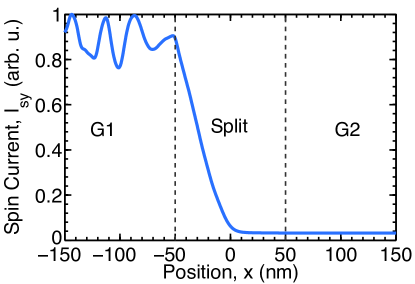
This is also consistent with the spatial variation of spin current along the device calculated using NEGF as shown in Fig. S1. Since there is no potential variation under the gates G1 and G2, there is no scattering and the spin current remains mostly conserved in these regions. The small oscillatory change in the G1 region is due to the interference created by the edge reflection in a finite-width device which is not included in the analytical model. The interference pattern can also be seen in the spin polarization plot in Fig. 2. On the other hand, inside the linear region, the electrons change direction which, in turn, results in a change in spin angular momentum. Therefore, spin current is not conserved. We also verified using NEGF that where, , and and are the total spin currents at source and drain, respectively. Therefore, the difference between the spin currents at the source and the drain terminal is the spin torque generated by the TIPNJ.
In our analytical model, the effects of non-zero inside the linear region are taken into account by constructing correct wave functions for the reflected and the transmitted waves. Given the correct wavefunctions, Eqs. (3) and (4) give correct spin currents everywhere for and (neglecting the small oscillation due to edge reflections) since the spin current is conserved in these regions. In NEGF, the effects of are taken into account automatically by the device Hamiltonian.
References
- Qi and Zhang (2011) X.-L. Qi and S.-C. Zhang, Reviews of Modern Physics 83, 1057 (2011).
- Cheianov and Fal’ko (2006) V. V. Cheianov and V. I. Fal’ko, Phys. Rev. B 74, 041403 (2006).
- Young and Kim (2009) A. F. Young and P. Kim, Nat Phys 5, 222 (2009).
- Sajjad et al. (2012) R. N. Sajjad, S. Sutar, J. Lee, and A. W. Ghosh, Physical Review B 86, 155412 (2012).
- Sajjad and Ghosh (2013) R. N. Sajjad and A. W. Ghosh, ACS nano 7, 9808 (2013).
- Wu et al. (2011) Z. Wu, F. Peeters, and K. Chang, Appl. Phys. Lett. 98, 162101 (2011).
- Takahashi and Murakami (2011) R. Takahashi and S. Murakami, Phys. Rev. Lett. 107, 166805 (2011).
- Wang et al. (2012) J. Wang, X. Chen, B.-F. Zhu, and S.-C. Zhang, Physical Review B 85, 235131 (2012).
- Datta et al. (2015) S. Datta, V. Q. Diep, and B. Behin-Aein, “What Constitutes a Nanoswitch? A Perspective,” in Emerging Nanoelectronic Devices, edited by A. Chen, J. Hutchby, V. Zhirnov, and G. Bourianoff (John Wiley and Sons, 2015) Chap. 2, p. 22.
- Liu et al. (2012) L. Liu, C.-F. Pai, Y. Li, H. W. Tseng, D. C. Ralph, and R. A. Buhrman, Science 336, 555 (2012).
- Datta et al. (2012) S. Datta, S. Salahuddin, and B. Behin-Aein, Applied Physics Letters 101, 252411 (2012).
- Mosendz et al. (2010) O. Mosendz et al., Phys. Rev. Lett. 104, 046601 (2010).
- Liu et al. (2011) L. Liu, T. Moriyama, D. C. Ralph, and R. A. Buhrman, Phys. Rev. Lett. 106, 036601 (2011).
- Mellnik et al. (2014) A. Mellnik et al., Nature 511, 449 (2014).
- Fan et al. (2014) Y. Fan et al., Nature Materials 13, 699 (2014).
- Gao et al. (2011) J.-H. Gao, J. Yuan, W.-Q. Chen, Y. Zhou, and F.-C. Zhang, Phys. Rev. Lett. 106, 057205 (2011).
- Manipatruni et al. (2014) S. Manipatruni, D. E. Nikonov, and I. A. Young, Applied Physics Express 7, 103001 (2014).
- Lee et al. (2014) J. Lee, J.-H. Lee, J. Park, J. S. Kim, and H.-J. Lee, Phys. Rev. X 4, 011039 (2014).
- Chen et al. (2010) J. Chen et al., Phys. Rev. Lett. 105, 176602 (2010).
- Burkov and Hawthorn (2010) A. A. Burkov and D. G. Hawthorn, Phys. Rev. Lett. 105, 066802 (2010).
- Tserkovnyak and Loss (2012) Y. Tserkovnyak and D. Loss, Phys. Rev. Lett. 108, 187201 (2012).
- Rashba (2003) E. I. Rashba, Phys. Rev. B 68, 241315 (2003).
- Tokatly (2008) I. V. Tokatly, Phys. Rev. Lett. 101, 106601 (2008).
- Sonin (2007) E. B. Sonin, Phys. Rev. Lett. 99, 266602 (2007).
- MAHFOUZI and NIKOLIĆ (2013) F. MAHFOUZI and B. K. NIKOLIĆ, SPIN 03, 1330002 (2013).
- Sun and Xie (2005) Q.-f. Sun and X. C. Xie, Phys. Rev. B 72, 245305 (2005).
- Yazyev et al. (2010) O. V. Yazyev, J. E. Moore, and S. G. Louie, Phys. Rev. Lett. 105, 266806 (2010).
- Hong et al. (2012) S. Hong, V. Diep, S. Datta, and Y. P. Chen, Phys. Rev. B 86, 085131 (2012).
- Zhang et al. (2009) Y. Zhang, T.-T. Tang, C. Girit, Z. Hao, M. C. Martin, A. Zettl, M. F. Crommie, Y. R. Shen, and F. Wang, Nature 459, 820 (2009).
- Stacey (1982) R. Stacey, Phys. Rev. D 26, 468 (1982).
- Susskind (1977) L. Susskind, Phys. Rev. D 16, 3031 (1977).
- Zainuddin et al. (2011) A. N. M. Zainuddin, S. Hong, L. Siddiqui, S. Srinivasan, and S. Datta, Phys. Rev. B 84, 165306 (2011).
- (33) See Eq. 8.6.5, p. 317 in S. Datta, Electronic Transport in Mesoscopic Systems, Cambridge University Press, Cambridge, England (1997).