Critical behavior at the dynamic Mott transition
Abstract
We investigate magnetoresistance of a square array of superconducting islands placed on a normal metal, which offers a unique tunable laboratory for realizing and exploring quantum many-body systems and their dynamics. A vortex Mott insulator where magnetic field-induced vortices are frozen in the dimples of the egg crate potential by their strong repulsion interaction is discovered. We find an insulator-to-metal transition driven by the applied electric current and determine critical exponents that exhibit striking similarity with the common thermodynamic liquid-gas transition. A simple and straightforward quantum mechanical picture is proposed that describes both tunneling dynamics in the deep insulating state and the observed scaling behavior in the vicinity of the critical point. Our findings offer a comprehensive description of dynamic Mott critical behavior and establish a deep connection between equilibrium and nonequilibrium phase transitions.
Mott insulators are systems that are expected to be metallic from the point of view of standard band theory but become insulators owing to correlations in the motions of electrons arising from their Coulomb repulsion. If the need of quantum particles to be delocalized to minimize the cost in kinetic energy from spatial confinement prevails over the Coulomb penalty, the system remains metallic. Imposing commensurate effects to restrict the freedom of particles to move, one can shift the balance towards localization and cause transition to insulating state PM:1937 ; Mott:1949 ; Mott:1990 ; Imada:1998 . As a practical matter, the transition can be realized by varying pressure or doping, i.e. tuning the carrier density, or by changing either temperature or electric field altering tunneling probability. The Mott insulator and Mott transition are an exemplary manifestation of quantum many-body physics of strongly correlated systems and are thought to be a key ingredient of high temperature superconductivity Lee:2006 , quantum phase transitions in a Bose-Einstein condensate and spin liquids Jaksch:1998 ; Hofstetter:2002 ; Greiner:2002 ; Bloch:2008 ; Jordens:2008 ; Sherson:2010 ; Weitenberg:2011 ; Watanabe:2012 , and be fundamental to metal-insulator-semiconductor field-effect transistors and related applications Nakano:2012 . Central to strongly correlated systems are becoming issues related to their non-equilibrium behavior, in particular, response to the electric field and the dielectric breakdown of Mott insulators Taguchi:2000 ; Rodichev:2013 ; Oka:2003 ; Eckstein:2010 destroying Coulomb localization. There has been extensive research that strives to describe delocalization and transition to metallic state caused by the electric field based on a many-body Schwinger-Landau-Zener mechanismOka:2003 ; Oka:2010 , nonequilibrium dynamical mean-field theory Eckstein:2010 , and time-dependent density-matrix renormalization-group simulations Heidrich:2010 . It succeeded to capture the existence of the threshold transition field and produce numerically a current-voltage dependence at modest fields. Yet many fundamental questions regarding dynamic Mott transition remain open. On experimental side, the observed electric field-induced destruction of the Mott insulator Rodichev:2013 , appears as a disorder-promoted avalanche-like breakdown along a percolation weak path, rather than a transformation of a gapped insulator spectrum into a metallic band-like. On the theoretical side, the employed approaches are valid at electric fields well below threshold breakdown field, but fail in the close vicinity of the transition. Here we address these challenges. We prepared an array of superconducting islands where magnetic field induced vortices are localized between the superconducting islands in the areas of weaker proximity-induced superconductivity, i.e. at the energy dimples of an egg crate potential Lobb-Review . If thermal fluctuations are not strong enough to overcome the combined localizing action of mutual repulsion and egg crate pinning, vortices form a vortex Mott insulating state at commensurate fields corresponding to an integer number of vortices per pinning site. The concept of the vortex Mott state was introduced in NelsVin:1993 and addressed in experiments on antidot arrays in superconducting films Baert:1995 ; Harada:1996 . Varying magnetic field provides precise control over the vortex number and tunes the ratio of the repulsion between vortices to their mobility note1 . Most importantly, in the structure of choice, it is the period of the superconducting islands array that takes up the role of the atomic spacing of an electronic system. As a result our nanopattern harboring vortices is free of detrimental effects of structural disorder inevitable in electronic systems. This enables us to observe an unconcealed insulator-to-metal transformation of the spectrum. Adopting a mean-field approximation we derive expressions for a dynamic response of a Mott insulator to the applied external drive asymptotically exact both at small applied fields and in close vicinity of the dynamic transition. The obtained formulas perfectly describe the experiment and reveal the connection between the equilibrium and nonequilibrium Mott behaviors.
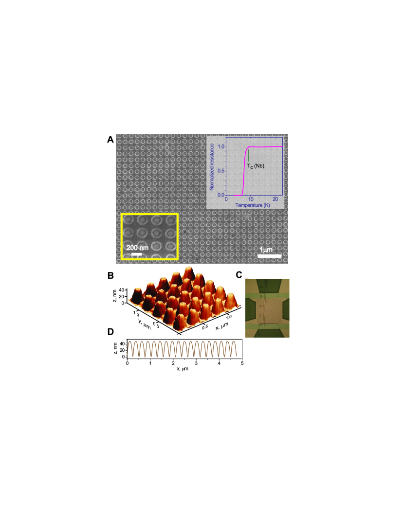
Our samples consist of 40 nm-thick Au, patterned as a four-point set-up in a Van der Pauw configuration for transport measurements, on Si/SiO2 substrates. The Au pattern is overlaid with a square array of superconducting niobium (Nb) islands 45 nm thick. An array contains 90,000 Nb islands placed with a period nm. The diameter of an island is nm and the island separation is nm. Panels A-D of Fig. 1 show scanning electron, atomic force microscopy, and optical images of the sample and the height profile along one of the principal axis of the array. The superconducting transition temperature of the array determined as the midpoint of the temperature resistance curve in the upper inset in Fig. 1A, is K which is 2 K lower than K of bulk niobium. This moderate downward shift of the transition temperature implies that the array is a strongly coupled network of superconducting islandsTinkham:1983 ; Baturina:2005 ; Mason:2012 .
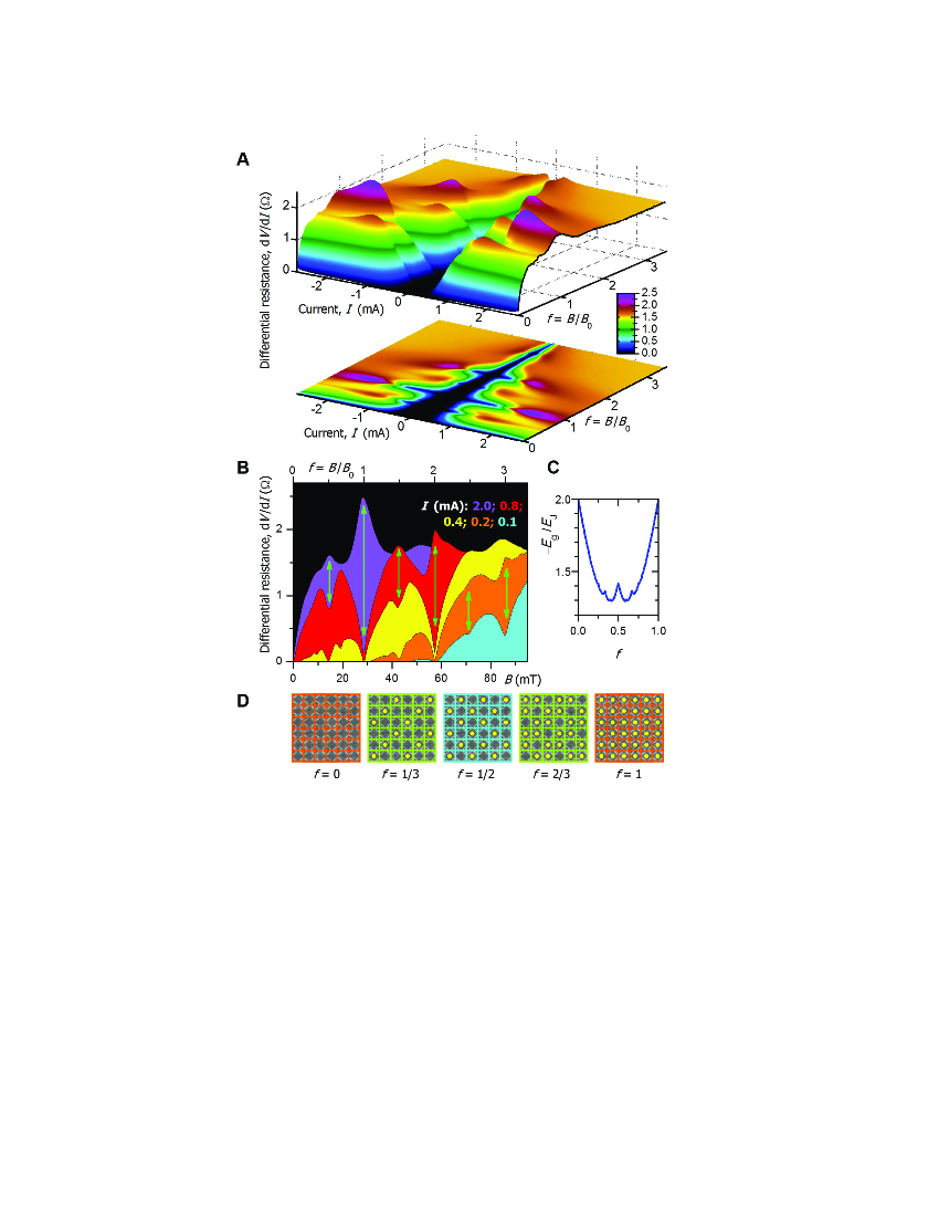
In order to identify the critical behavior of the dynamic Mott transition we perform transport measurements in the current-voltage-magnetic field (,,) three-coordinate space scanning and in small steps. The measurements are carried out in a shielded cryostat at temperature K which is much lower than . To probe the density of mobile states of the vortex system the differential resistance, , is usedDeshpande:2009 ; notezero . Panel A of Fig. 2 shows colour plots of the differential resistance as function of the applied current and the magnetic field in units of frustration parameter , where , and is the magnetic flux quantum. In our array mT. The data presented in Fig. 2A enable a meaningful scaling analysis which will reveal the nature of the Mott insulator-to-metal transition in the dynamic regime. To highlight the transition we display representative isocurrent cuts as vs. plots in Fig. 2B. At modest currents we reveal a wealth of dips in at integer frustrations, namely at 1, 2 and 3 corresponding to integer number of flux quanta per elemental square of an array, as well as a fine structure of fractional dips at 1/3, 1/2, 2/3, 4/3, 3/2, … . These minima reflect the modulation of the ground state energy due to formation of periodic vortex patterns in a magnetic field (Fig. 2C,D). The dips in the resistance and singularities in magnetization at commensurate (but mostly integer) frustrations due to modulations of were conventionally observed in numerous experiments on Josephson junction-, proximity-, and antidot arrays, and superconducting wire networks, seeBaturina:2011 and references therein. Importantly, the very observation of minima at fractional evidences the high precision periodicity of our array. Indeed, while the oscillations with the main period, corresponding to integer , are robust, the modulations at fractional require fine synchronization of superconducting phase in several overlapping contours (see how shallow the corresponding energy minima in Fig. 2C are) and are easily destroyed by even slight irregularities in the array parameters.
The dependence playing a fundamental role in superconducting regular systems is an energy band edge of the full energy spectrum [known as Hofstadter’s butterflyHofstadter:1976 ] of the Harper equation Harper:1955 ; Rammal:1984 ; Baturina:2011 . This is the same spectrum that arises for tight-binding electrons restricted to a two-dimensional square lattice under a magnetic field perpendicular to the plane and which is the signature of a fractional quantum Hall effectDean:2013 . The identity of the spectra is a manifestation of the duality between vortices and electrical charges NelsVin:1993 ; Shahar:1996 . Viewing Fig. 2D as a visualization of Mott-Hubbard model for electrons the case would correspond to a single particle per site. Accordingly, for its vortex counterpart, the case of complete filling of the pinning sites array () was conjectured to form a vortex Mott insulatorNelsVin:1993 ; Nelson:1998 . Our data enable us to extend this conjecture onto fractional filling and propose a fractional Mott insulator, a mirror image of fractional quantum Hall states. The profound low current minima in at rational support this conclusion.
Our key observation is a reversal of the minima in at rational into maxima upon increasing the current bias, which, as we show below by scaling analysis, is a direct manifestation of the existence of the vortex Mott insulator and its transition into a metallic state. We reveal a reach collection of reversals at commensurate fields 1/3, 1/2, 2/3, 1, … with the most pronounced effects being seen at integer and half-integer frustration factors (Fig. 2B). The relative strength of the reversal effect follows the respective depths of the minima at moderate currents. Similar minima-to-maxima flips themselves were observed in regular superconducting systems of different geometries, namely, in a proximity array Benz:1990 and in an antidote arrayJiang:2004 , where models associated with vortex depinning were provided.
The vortex Mott insulating behavior manifests itself as the tendency to downward divergence of the traces on approach to . Remarkably, upon the vortex Mott insulator-to-metal transition with the increasing current, an upward divergence of traces marks the profound metallic-like behavior near . Notably, the dip-to-peak evolution upon increasing current is observed only in , but not in the quantity responsible for the dissipation (see fig. S1). This rules out pure dissipative mechanisms due to depinning as possible origin of the flips in Benz:1990 ; Jiang:2004 .
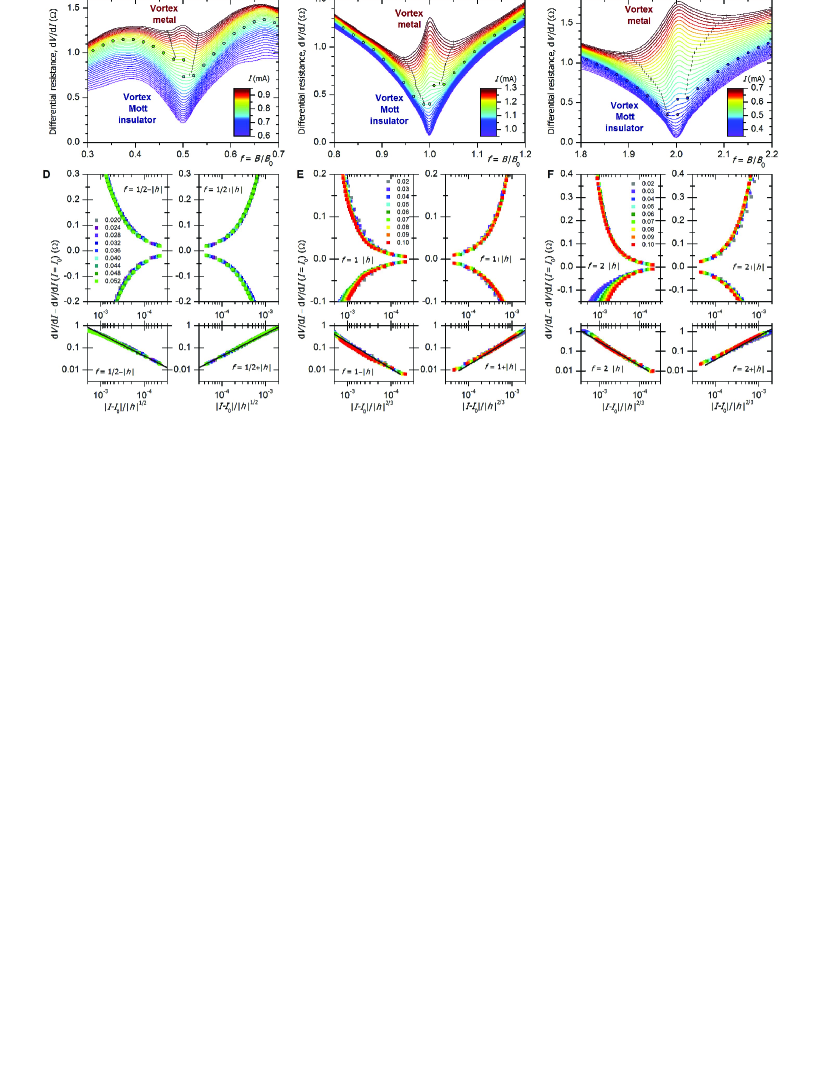
We present detailed plots of vs. curves in the vicinity of in the critical region in the upper row panels of Fig. 3. There is an asymmetry between the left-hand and right-hand vicinities of the commensurability points so that they have to be considered independently. In either of them there is an apparent separatrix between insulating-like and metallic-like regions. We identify the currents corresponding to separatrices between insulating and metallic behavior as critical currents at which the dynamic Mott transition occurs, and find them from the condition (asymmetry between may reflect the asymmetry between the ‘particle’ and ‘hole’ tunneling dynamics near commensurate values of frustration parameter, and parallels the asymmetry between transition temperatures of electrons- and holes-doped Mott insulators Segawa:2010 ). These separatrices are highlighted by dots in Fig. 3A-C. For the respective traces display minima, marked by strokes in Fig. 3A-C encompassing the region of metallic behavior. These critical regions widen upon increasing current similar to the standard quantum phase transition critical region which increases with growing temperature Sondhi:1997 . That and are different implies also that in the current intervals at exactly commensurate values , Mott insulating and metallic phases coexist Kotliar:1999 .
Now we turn to critical vicinity of the Mott transition critical point, . A scaling theory states that in the critical region of the continuous phase transition physical observables follow the scaling laws, so that their respective correlation lengths diverge on approach to the critical point Kadanoff:1967 ; Fisher:1974 . The Mott insulator-to-metal transition is driven by tuning the ratio between the repulsion strength and the characteristic tunneling energy (bandwidth), . Accordingly, the static Mott transition exhibits scaling behavior with respect to temperature, and the repulsion strength . The mean-field version of the Hubbard model predicts Kotliar:2000 that near the Mott critical point , where and are critical temperature and critical particle repulsion strength, respectively, the deviation should scale as , where is the exponent relating the scaling of the source field with the order parameter. To find the critical behavior of the dynamic vortex Mott transition, we note that the role of is taken by the magnetic field which sets the vortex density and, as such, controls the vortex repulsion. Drawing inspiration from the theory of nonequilibrium critical fluctuations near a dynamic phase transitionChtchelk:2009 which found that the equilibrium singular behavior with respect to turns into a singular behavior with respect to deviation from the critical value of applied bias, we conjecture the following mapping of the critical behavior of the static Mott transition to that of dynamic vortex Mott transition: , , and the critical point yielding critical scaling . To show the validity of this assumption we scale our data into the universal form
| (1) |
taking the exponent as an adjustable fitting parameter. The best collapse of the data onto a single curve near is achieved at (Fig. 3D). Importantly, the independent scaling procedures at both, the left- and right-hand sides of the critical frustration yield the same value of , despite that separatrices are different. The same procedure for the left- and right-hand sides of and 2 gives rise to (Fig. 3E,F). Double-logarithmic plots in the vicinity of the above values of display a power-law functional form of , as shown in the lower panels of Fig. 3D-F. For we find . For both and we find for all four plots. The revealed universal scaling properties of the current and magnetic field dependent differential resistance, following Eq. 1, experimentally establishes the dynamic vortex Mott transition and the existence of the vortex Mott insulator in superconducting networks.
To gain insight into the observed scaling behaviors and in how nonequilibrium carriers that are frozen into a Mott insulator start to move in response to external drive, we first consider an electronic Mott insulator. The applied electric field stimulates tunneling current which quantifies the rate of the decay of the insulating ground state, i.e. dielectric breakdown of the insulator. The latter occurs via formation of an elemental nucleus of the metallic phase of the linear size of the order of the electron wavelength and with the characteristic energy ( is the atomic spacing of the material). Then the current , where is an electron charge. The elemental volume of an insulator contains electronic states, where is the Mott insulating gap due to Coulomb interactions and is the electronic density of states at the Fermi level. The minimal energy that each state should acquire to become metallic, i.e. delocalized, is the energy equal to insulating gap . Thus the nucleation energy . Remembering that , where is the Fermi velocity, we find , where the threshold breakdown field . Our expression is exactly the decay rate of the ground Mott state obtained by the numerical fit of the dynamics of the one-dimensional Hubbard model Oka:2003 ; Oka:2010 ; Eckstein:2010 ; Heidrich:2010 to the Landau-Zener quantum tunneling formula at . On approach to the threshold field where and the Mott gap vanishes, the barrier for the electron acquires a parabolic shape with the height proportional to LO:1986 . Using the exact formula for the transparency of the parabolic barrier LL:1977 , we find the resulting tunneling current as .
To describe a vortex Mott insulator we use the duality between vortices and charges Fazio:1991 ; vanWees:1991 ; NelsVin:1993 ; Nelson:1998 and replace the electric field driving electrons by the applied current dragging vortices. Correspondingly, the current, which is a response of the electronic system, we substitute by the voltage induced by moving vortices. As a result the - curves describing the response of a vortex Mott insulator to the applied current read
| (2) |
where is a threshold breakdown current at which a vortex Mott insulator transforms into a metallic phase. One sees that the characteristic energy controlling the response of the vortex system near the Mott transition scales as , which explains the origin of the experimentally observed scaling for integer frustrations. Note that near the breakdown threshold the transparency of the tunneling barrier depends crucially on its shape near the top. Since the barriers governing the breakdown at fractional frustrations may differ from those at integer ones, the derivation of fractional critical exponents requires special analysis.
We now discuss the implications of our results. Using an artificially engineered array of superconducting islands to materialize a vortex Mott insulator, enables us to observe the dynamic Mott transition from an insulating to a metallic state as the current-induced transformation of the insulator gapped spectrum into the metallic-like one. Notably, our value of for the integer dynamic vortex Mott transition coincides with the mean-field value of for the temperature-pressure driven thermodynamic Mott transition Limelette:2003 ; note . The latter was found to belong in the class of the liquid-gas transition of classical systems Kadanoff:1967 ; Kotliar:2000 ; Limelette:2003 (the insulating phase is associated with a “gas” phase while the metallic phase corresponds to a “liquid”). The universal scaling properties of the current- and magnetic field-dependent dynamical resistivity experimentally demonstrate that vortex Mott insulator also undergoes a liquid-gas-like phase transition at the nonequilibrium Mott critical endpoint. This reveals a deep correspondence between the dynamic and thermodynamic Mott transitions and supports the earlier conjecture that the external drive takes the role of effective temperature in far-from-equilibrium systems Chtchelk:2009 .
Quantum mechanical vortex-particle mappingNelsVin:1993 enables straightforward transcription of the results for thermally activated vortex Mott dynamics onto quantum Mott dynamics of electrons and cold atoms. The mapping is achieved by substitutions and , where is the size of the system along the magnetic field (i.e. the vortex) direction. This makes our system an irreplaceable high-precision laboratory for studying dynamic Mott behaviors in quantum systems at easily accessible moderate temperatures.
Turning to the difference between critical exponents at integer and fractional frustration parameters ( for and for ) note that an integer vortex Mott insulator corresponds to full filling of the sites. This state can be viewed as a ‘ferromagnetic’ state and belongs in the Ising universality class. On the other hand, the case of represents an ‘antiferromagnetic’ state since the direction of currents in “empty” cells corresponds to vortices of the opposite direction, fig. S2. Thus, the critical behavior of these two distinct vortex Mott insulating phases belongs in different universality classes with different exponents. Finally, the energy spectrum of the fractional vortex Mott insulator shown in Fig. 2C is the Hofstadter butterfly spectrum of the Harper equation Hofstadter:1976 , which is also the spectrum of the fractional quantum Hall electronic state Dean:2013 . This correspondence between the fractional vortex Mott insulating- and fractional quantum Hall electronic states offers ‘vortex-side’ evidence for the charge-flux duality previously observed near the quantum Hall liquid to insulator transition Shahar:1996 . The gained insights open a route to in-depth investigation of dynamic phase transitions in strongly correlated fermionic and bosonic systems using the tunable vortex systems.
Acknowledgements: We thank R. Wiegerink for help and discussion about programming with CleWin software. We thank T. Jenneboer for providing the electron beam lithography. We thank Gerben Hopman, Pim Reith, Frank Roesthuis and Dick Veldhuis for help and support during the experiments. N.P. thanks Alessandro Ricci, Gaetano Campi and Antonio Bianconi for valuable discussions. The work was supported by the Dutch FOM and NWO foundations, the Russian Academy of Sciences, the Russian Foundation for Basic Research (Grant No. 12-02-00152), the Ministry of Education and Science of the Russian Federation, and by the U.S. Department of Energy, Office of Science, Materials Sciences and Engineering Division. N.P acknowledges for financial support the Marie Curie IEF project FP7-PEOPLE-2012-IEF-327711-IMAX.
Supporting Materials
Methods
Standard photolithographic tools have been employed to create a 40 nm thick Au template (see Fig. 1) on a Si/SO2 substrate of 1 1 cm2. The template consists of a central square of 82 82 m2, with the corners connected to 4 terminals for electric measurements (not visible in figure). The size of the terminals is 200 200 m2, large enough for micro bonding. The Nb pattern is then created on top of the central Au square employing electron beam lithography and DC sputtering, via a standard PMMA lift off procedure. In this way the electrical conduction among the Nb islands can take place via the Au template that lies underneath. The resulting Nb array is 80 80 m2 large and comprises 300 300 sites. The Nb island on each site has a diameter of nm and is nm thick. The average distance between the islands is nm. We performed 4-point probe resistivity measurements to determine the superconducting transition temperature. To ensure a uniform current injection into the array, two 45 nm Nb bus bars are deposited along two opposite sides of the array, as shown in Fig. 1C; the gap between strips and array is less that 0.5 m. When cooled below 9 K, the bars become superconducting and effectively short the corresponding current and voltage leads. This results in a 2-point measurement that yields magnetoresistance data shown in Fig. 2. The measurements are carried out in a shielded cryostat at 1.4 K. A current bias is applied using a ramp generator at several Hz. The measured voltage waveform is amplified using homebuilt low-noise electronics, and subsequently digitized with a National Instruments PXI-4461. The characteristics are non-hysteretic and averaged over several current cycles. The dynamic resistance is found by numerically differentiating the averaged characteristics. A magnetic field is applied by placing a solenoid around the sample with the field perpendicular to the sample plane. The current through the solenoid increases in a stepwise fashion and separate traces are recorded at each field step. The obtained curves are nonlinear, similar to superconducting junction characteristics but with a residual resistance. This resistance corresponds to the finite distance between the superconducting bus bars and the Nb island array.
Differential resistance and resistance
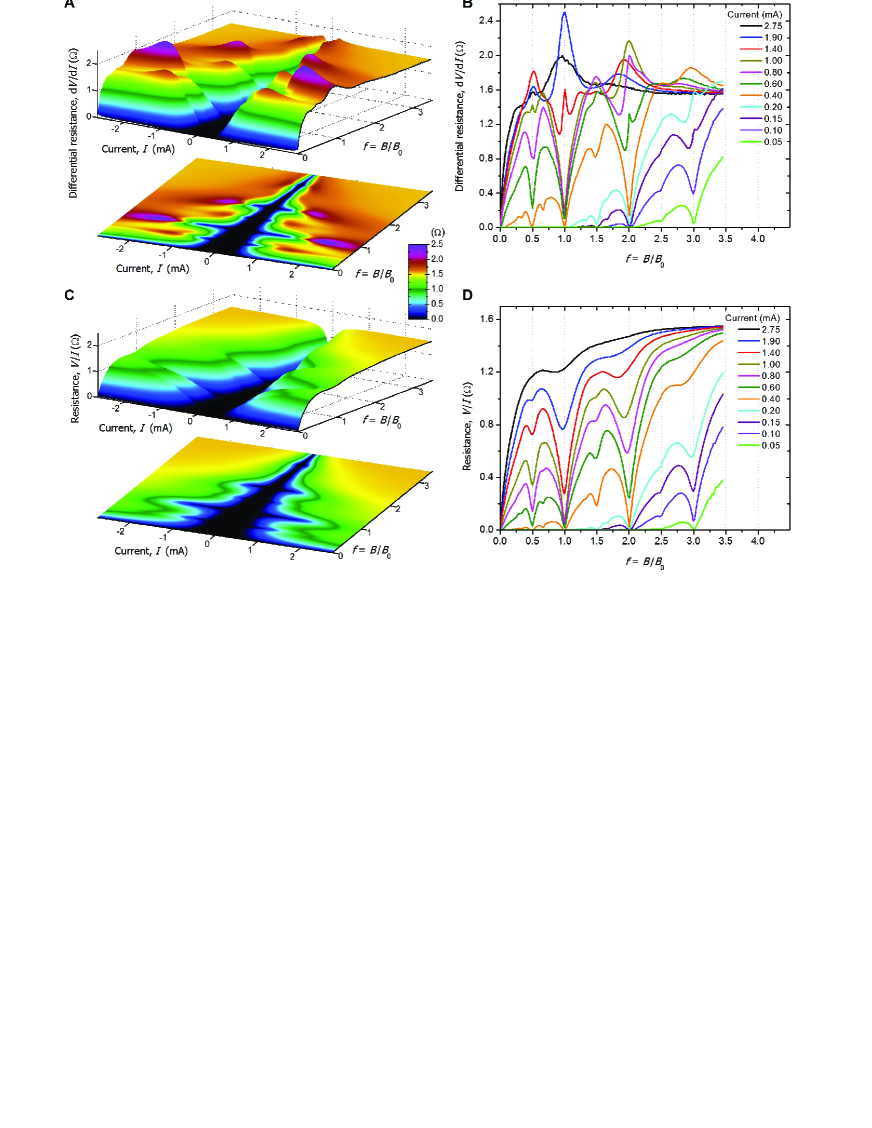
Figure S1 shows the same set of data as in the main text, Fig. 2A, presented as differential resistance, panels (A) and (B), and as a resistance, panels (C) and (D). All the measurements were performed under the dc applied current. Several important comments are in order:
(i) The reaches much larger values than the corresponding values of the resistance, as clearly seen in the color plots.
(ii) Dip-to-peak evolution at rational upon the increasing current is experienced only by but not by the resistance.
(iii) As the measurements are carried out under the constant currents, the plots for the resistances coincide up to the numerical factor, , with the plots for the dissipated power. Upon increasing current the dissipation grows, as it should, since small pinning barriers are washed up by larger drives. At the same time the magnitude of the dissipation still exhibit local minima at rational as is clearly demonstrated by almost all curves at panel (D).
‘Ferromagnetic’ and ‘antiferromagnetic states’
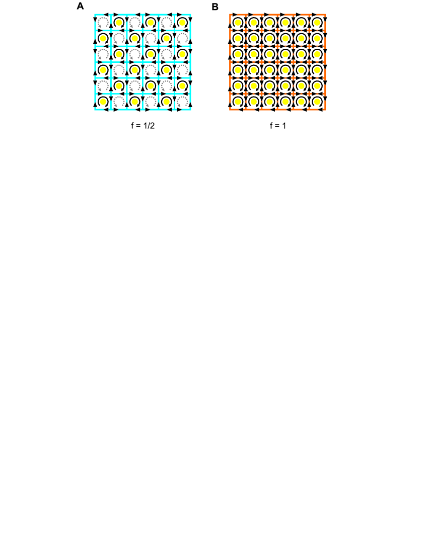
Figure S 2 shows current distribution in the proximity network corresponding to the half-integer, , and integer, , filling. At the distribution of currents correspond to alternating vortices of opposite direction and therefore is referred to as an “antifferromagnetic” state. Accordingly, the state with can be viewed as the “ferromagnetic” one. The current distributions at and the ground states for vortices trapped in the egg-crate potential relief are described in detail in a review by NewrockLobb-Review Since antiferromagnetic and ferromagnetic states belong in different universality classes one expects the scaling exponents characterizing the behaviour of the order parameter to differ.
References
- (1) N. F. Mott, R. Peierls, Discussion of the paper by de Boer and Verwey. Proc. Phys. Soc. 49 (4S), 72-73 (1937).
- (2) N. F. Mott, The Basis of the Electron Theory of Metals, with Special Reference to the Transition Metals. Proc. Phys. Soc. A 62, 416-422 (1949).
- (3) N. F. Mott, Metal-Insulator Transitions (Taylor and Francis, London, 1990).
- (4) M. Imada, A. Fujimori, Y. Tokura, Metal-insulator transitions. Rev. Mod. Phys. 70, 1039-1263 (1998).
- (5) P. A. Lee, N. Nagaosa, X.-G. Wen, Doping a Mott insulator: Physics of high-temperature superconductivity. Rev. Mod. Phys. 78, 17-85 (2006).
- (6) D. Jaksch et al., Cold Bosonic Atoms in Optical Lattices. Phys. Rev. Lett. 81, 3108-3111 (1998).
- (7) W. Hofstetter, J. I. Cirac, P. Zoller, E. Demler, M. D. Lukin, High-Temperature Superfluidity of Fermionic Atoms in Optical Lattices. Phys. Rev. Lett. 89, 220407 (2002).
- (8) M. Greiner, O. Mandel, T. Esslinger, T. W. Hänsch, and I. Bloch, Quantum phase transition from a superfluid to a Mott insulator in a gas of ultracold atoms. Nature 415, 39-44 (2002).
- (9) I. Bloch, J. Dalibard, W. Zwerger, Many-body physics with ultracold gases. Rev. Mod. Phys. 80, 885-964 (2008).
- (10) R. Jördens, N. Strohmaier, K. Günter, H. Moritz, T. Esslinger, A Mott insulator of fermionic atoms in an optical lattice. Nature 455, 204-207 (2008).
- (11) J. F. Sherson et al., Single-atom-resolved fluorescence imaging of an atomic Mott insulator. Nature 467, 68-72 (2010).
- (12) C. Weitenberg et al., Single-spin addressing in an atomic Mott insulator. Nature 471, 319-324 (2011).
- (13) D. Watanabe et al., Novel Pauli-paramagnetic quantum phase in a mott insulator. Nature Comm. 3, 1090 (2012).
- (14) M. Nakano, et al., Collective bulk carrier delocalization driven by electrostatic surface charge accumulation. Nature 487, 459-462 (2012).
- (15) Y. Taguchi, T. Matsumoto, Y. Tokura, Dielectric breakdown of one-dimensional Mott insulators Sr2CuO3 and SrCuO2. Phys. Rev B. 62, 7015-7018 (2000).
- (16) V. Guiot et al., Avalanche breakdown in GaTa4Se8-xTex narrow-gap Mott insulators. Nature Comm. 4, 1722 (2013).
- (17) T. Oka, R. Arita, H. Haoki, Breakdown of a Mott Insulator: A Nonadiabatic Tunneling Mechanism. Phys. Rev. Lett. 91, 066406 (2003).
- (18) M. Eckstein, T. Oka, P. Werner, Dielectric Breakdown of Mott Insulators in Dynamical Mean-Field Theory. Phys. Rev. Lett. 105, 146404 (2010).
- (19) T. Oka, H. Aoki, Dielectric breakdown in a Mott insulator: Many-body Schwinger-Landau-Zener mechanism studied with a generalized Bethe ansatz. Phys. Rev. B 81, 033103 (2010).
- (20) F. Heidrich-Meisner et al., Nonequilibrium electronic transport in a one-dimensional Mott insulator. Phys. Rev. B 82, 20511 (2010).
- (21) R. S. Newrock, C. J. Lobb, U. Geigenmüller, M. Octavio, The Two-Dimensional Physics of Josephson Junction Arrays. Solid State Phys. 54, 263-512 (2000).
- (22) D. R. Nelson, V. M. Vinokur, Boson localization and correlated pinning of superconducting vortex arrays. Phys. Rev. B48, 13060-13097 (1993).
- (23) M. Baert et al. Composite Flux-Line Lattices Stabilized in Superconducting Films by a Regular Array of Artificial Defects. Phys. Rev. Lett. 74, 3269-3272 (1995).
- (24) K. Harada et al. Direct Observation of Vortex Dynamics in Superconducting Films with Regular Arrays of Defects Science, 274, 1167-1170 (1996).
- (25) The vortex density and, therefore the strength of their interaction is proportional to the magnetic field. At the same time magnetic field suppresses Josephson coupling between the islands and thus diminishes the tunneling barrier.
- (26) M. Tinkham, D. W. Abraham, and C. J. Lobb, Periodic flux dependence of the resistive transition in two-dimensional superconducting arrays. Phys.Rev. B 28, 6578-6581 (1983).
- (27) T. I. Baturina, Yu. A. Tsaplin, A. E. Plotnikov, and M. R. Baklanov, Anomalous Behavior near Tc and Synchronization of Andreev Reflection in Two-Dimensional Arrays of SNS Junctions. JETP Lett. 81, 10-14 (2005).
- (28) S. Eley, S. Gopalakrishnan, P. M. Goldbart, N. Mason, Approaching zero-temperature metallic states in mesoscopic superconductor-normal-superconductor arrays. Nature Phys. 8, 59-62 (2012).
- (29) In an electronic Mott insulator the density of states is probed by the differential conductivity, Deshpande:2009 . In the insulating state the density of states has a dip at zero bias. Upon the transition to a metallic state it turns into a peak. In a vortex system, according to the quantum mechanical mapping correspondenceNelsVin:1993 , the differential conductance is substituted by the differential resistance.
- (30) V. V. Deshpande et al., Mott Insulating State in Ultraclean Carbon Nanotubes. Science 323, 106-110 (2009).
- (31) D. R. Hofstadter, Energy levels and wavefunctions of Bloch electrons in rational and irrational magnetic fields. Phys. Rev. B 14, 2239-2249 (1976).
- (32) P. G. Harper, Single Band Motion of Conduction Electrons in a Uniform Magnetic Field. Proc. Phys. Soc. A 68 874-878 (1955).
- (33) B. Pannetier, J. Chaussy, R. Rammal, and J. C. Villegier, Experimental Fine Tuning of Frustration: Two-Dimensional Superconducting Network in a Magnetic Field. Phys. Rev. Lett. 53, 1845-1848 (1984).
- (34) T. I. Baturina et al., Nanopattern-stimulated superconductor-insulator transition in thin TiN films. Europhys. Lett. 93, 47002 (2011).
- (35) C. R. Dean et al., Hofstadter’s butterfly and the fractal quantum Hall effect in moiré superlattices. Nature 497, 598-602 (2013).
- (36) D. Shahar, D. C. Tsui, N. Shayegan, E. Shimshoni, S. L. Sondhi, Evidence for Charge-Flux Duality near the Quantum Hall Liquid-to-Insulator Transition. Science 274, 589-592 (1996).
- (37) R. A. Lehrer, D. R. Nelson, Vortex pinning and the non-Hermitian Mott transition. Phys. Rev. B 58, 12385-12402 (1998).
- (38) S. P. Benz, M. S. Rzchowski, M. Tinkham, C. J. Lobb, Critical currents in frustrated two-dimensional Josephson arrays. Phys. Rev. B 42, 6165-6171 (1990).
- (39) Z. Jiang et al. Pinning phenomena in a superconducting film with a square lattice of artificial pinning centers. App. Phys. Lett. 84, 5371-5373 (2004).
- (40) K. Segawa et al. Zero-doping state and electron–hole asymmetry in an ambipolar cuprate. Nature Physics, 6, 579-583 (2010).
- (41) S. L. Sondhi, S. M. Girvin, J. P. Carini, D. Shahar, Continuous quantum phase transitions. Rev. Mod. Phys. 69, 315-333 (1997).
- (42) M. J. Rozenberg, R. Chitra, G. Kotliar, Finite Temperature Mott Transition in the Hubbard Model in Infinite Dimensions. Phys. Rev. Lett. 83, 3498 (1999).
- (43) L. P. Kadanoff et al., Static Phenomena Near Critical Points: Theory and Experiment. Rev. Mod. Phys. 39, 395-431 (1967).
- (44) M. E. Fisher, The renormalization group in the theory of critical behavior. Rev. Mod. Phys. 46, 597-616 (1974).
- (45) G. Kotliar, E. Lange, M. J. Rozenberg, Landau Theory of the Finite Temperature Mott Transition. Phys. Rev. Lett. 84, 5180-5183 (2000).
- (46) N. Chtchelkatchev, V. Vinokur, Nonequilibrium mesoscopic superconductors in a fluctuational regime. Europhys. Lett. 88, 47001 (2009).
- (47) A. I. Larkin, Yu. N. Ovchinnikov, Resonance Reduction of the Lifetime of the Metastable State of Tunnel Junctions. Journ. Low Temp. Phys. 63, 317-329 (1986).
- (48) L. D. Landau, E. M. Lifshitz, Quantum mechanics. Elsevier, Oxford, (1977)
- (49) R. Fazio, G. Schön, Charge and vortex dynamics in arrays of tunnel junctions. Phys. Rev. B 43, 5307-5320 (1991).
- (50) B. J. van Wees, Duality between Cooper-pair and vortex dynamics in two-dimensional Josephson-junction arrays. Phys. Rev. B 44, 2264-–2267 (1991).
- (51) In the equilibrium case the critical behavior is demonstrated inLimelette:2003 by scaling of the conductivity as function of temperature and the applied pressure (serving to change the electron density) in a form (the ‘effective field’ , and were spinodal and critical pressures, respectively, and ).
- (52) P. Limelette et al., Universality and Critical Behavior at the Mott Transition, Science 302, 89-92 (2003).