Josephson effect and Andreev reflection in Ba1-xNaxFe2As2 (=0.25 and 0.35) point contacts
Abstract
characteristics and their first derivatives of ScS and ScN-type (S–superconductor, c–constriction, N–normal metal) point-contacts (PCs) based on Ba1-xNaxFe2As2 (=0.25 and 0.35) were studied. ScS-type PCs with S=Nb,Ta and Pb show Josephson-like resistively shunted curves with microwave induced Shapiro steps which satisfy relation 2. The product (–critical current, – normal state PC resistance) in these PCs is found to be up to 1.2 mV. All this data with the observed dependence of the on the microwave power of ScS PCs with Pb counterelectrode indicates the presence of the singlet s-wave type pairing in Ba1-xNaxFe2As2. From the curves of ScN-type PCs demonstrating Andreev-reflection like features, the superconducting gap ratio 2kBTc = 3.61 for the compound with =0.35 was evaluated. Analysis of these at high biases , that is well above , testifies transition to the thermal regime in PCs with a voltage increase.
pacs:
74.50.+r, 74.70.Dd, 74.45.+cI INTRODUCTION
The discovery of superconductivity in the iron-based materials provokes an enormous interest, since a high was obtained in compounds with ferromagnetic metals, what raised the question about nature of superconducting (SC) pairing mechanism and symmetry of SC wave function. Ferriferous doped superconductors of 122-type structure based on the parent compound BaFe2As2 are the most investigated pnictide systems nowadays. Hole doping by alkali metals leads to the suppression of the spin-density wave antiferromagnetic state and the appearance of superconductivity with transition temperature up to 38 K Rotter2008 ; Sasmal . Superconductivity is formed here in a multi-band system with multiple Fermi surfaces of different (electron and hole) nature, which is very different from the single band situation in high- cuprates. Since their discovery, quite a lot of research has been done, in which the electron spectrum and the Fermi surface of new superconductors were studied using angle-resolved photoemission (ARPES) Kordyuk . This method has proved its effectiveness in the physics of high- cuprates. In fact, for iron-based superconductors ARPES-study provides valuable information that helps clarify the peculiarities of their electronic spectrum, as well as of the Fermi surface, and the quantities and characteristics of SC gap(s). Investigation of the Josephson effect Seidel and point-contact Andreev-reflection (PCAR) spectroscopy Daghero2011 plays significant role in the understanding of the nature of the SC ground state in these material as well.
The Josephson effect KY ; Barone was investigated in pressure-type contacts with the Pb counterelectrode in Zhang09 . Stable Josephson coupling in contacts Ba1-xNaxFe2As2–Pb along the c-axis was found. It was established that a Josephson current flows mainly through the active small contacts which exhibit virtually no superconductivity at low clamping. Just as the pressure increases, the contact area increases and superconductivity appears. Observation of the Josephson effect in the c-axis geometry in this iron pnictides excludes pure p- or d-wave pairing in these materials and the obtained results support the existence of s-wave pairing Zhang09a . Josephson junctions fabricated in epitaxial films utilizing bicrystal grain boundary Katase and oxidized titanium layers as barriers Doring have been studied as well. Both studies report also some difficulty to get junctions with Josephson behaviour and the product is up to several orders of magnitude less than that expected theoretically, what is a serious obstacle for an application.
On the other hand, PCAR spectroscopy is widely used to study SC order parameter(s) or SC gap(s) in these compounds Daghero2011 ; Szabo ; XinLu . In our previous paper NaidyukBanafeas we utilized the PCAR spectroscopy to study the SC gap in the sample with =0.25. It was shown that pronounced peculiarities in the PC spectra at high biases above the SC gap is governed by high specific resistivity and thermopower of the bulk material being the features of the thermal regime of the current flow in PCs. Whereas emerging of AR structures at small biases gave possibility for the spectroscopy of the SC gap which showed unequivocally only one gap with the preferred value 2k6. In this study we continue PCAR investigation of the Ba1-xNaxFe2As2 family, focusing on the compound with =0.35, in order to have a look on the gap structure in this compound and compare with the results obtained in NaidyukBanafeas for =0.25.
II EXPERIMENTAL DETAILS
Single crystals of Ba1-xNaxFe2As2 were grown using a self-flux high temperature solution growth technique Aswartham . For the samples with = 0.25 and 0.35 the SC transition in resistivity starts around 10 and 34 K, correspondingly.
The PCs were established in situ by touching a thin metallic wire (Ø0.2–0.3 mm) to the cleaved (at room temperature) surface (an edge) of the plate-like (flake) sample. Thus, we measured heterocontacts between simple metal and the title compound preferably in the -plane. The differential resistance of characteristic of PC was recorded by sweeping the dc current on which a small ac current was superimposed using standard lock-in technique. The measurements were performed mainly at the temperature 4.2 K (up to 35 K in some cases) and under microwave irradiation with frequency 9.57 GHz in the case of ScS contacts.
The critical current (Josephson effect) was registered on curves of ScS contacts only after electrical breakdown of mechanically established PC from resistance of a few tenth Ohm till much lower resistance, i.e. much less than 1. For PCs with Pb counterelectrode we were able to produce Josephson junction with a clear critical current or zero resistance at =0, while in the case of the Ta and Nb counterelectrodes an additional resistance appeared, so that .
The characteristic voltage ( is normal state resistance of PC) that determines the cutoff frequency of the Josephson current Likharev , was up to =1.2 meV for the PCs with Pb counterelectrode. Induced Shapiro steps were observed under microwave irradiation both on curves and more clearly on their first derivatives with the distance between them .
For some ScS contacts with the Pb counterelectrode, as well as for all contacts with the Ta counterelectrode, the critical current was very small and the manifestation of the Josephson effect (Shapiro steps) was observed only on the first derivatives of the . Equivalent circuit for PCs in this case, can be represented as a series connection of the resistance with a Josephson junction. In the case of Nb counterelectrode a more complex circuit was implemented with serial and parallel additional resistances as it will be shown further.
III RESULTS AND DISCUSSION
III.1 Search for Josephson effect in ScS contacts
Figure 1 shows a series of the curves and first derivative of a ScS PC Ba1-xNaxFe2As2 with Pb counterelectrode at different microwave power levels. It is noticeable that under irradiation a stepped structure occurs in the . This is, so-called, Shapiro steps, or manifestation of the Josephson effect KY ; Barone .
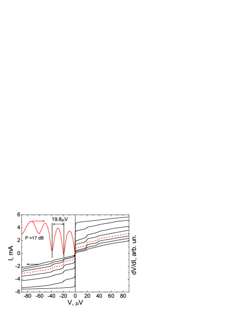
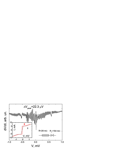
For some contacts with the Pb counterelectrode (Fig. 2) there was a significant slope of at =0 and the critical current was small. This leads to the fact that the distance between the steps becomes larger than the expected one. The slope at =0 indicates the inclusion of an additional resistance in series with the Josephson junction (see the equivalent circuit in Fig. 2). Accounting of this resistance (=28 m) leads to the elimination of inclination at =0 (Fig. 2 inset), while appropriate distance between steps Shapiro becomes as it should be in the case of Josephson coupling. It should be noted that the induced current step with the largest number was observed at mV. This value coincides with the characteristic voltage estimated from the product of .
The position of current steps on the voltage axis is defined by the Josephson relation KY ; Barone :
| (1) |
with a superconducting pair charge equal to 2e. It is known KY ; Barone that the height of the current steps induced by the external field oscillates with increase of the irradiation power. The amplitude of the current steps is given by the Bessel function of the corresponding order KY ; Barone :
| (2) |
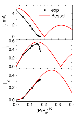
where ( is microwave power) is voltage induced in a contact by microwave field. Fig. 3 shows dependence of the critical current and the first two steps of currents and on the microwave power. The resulting curves are in good agreement with the initial portions of the corresponding Bessel functions Barone . Since the investigated Josephson junctions have low resistance (R) then we do not have enough microwave power to trace the behavior of the critical current and the first two steps of the currents and to a greater extent.
In the case of the Ta counterelectrode, electrical breakdown is also used to create a Josephson junction. However, in this case, there was always a significant slope of at =0 and thus the critical current was negligible. This leads to the observation that Shapiro steps become visible only on the first derivative as dips and the distance between them was greater than the expected one (Fig. 3). Thus, for the ScS contacts with the Ta counterelectrode the equivalent circuit includes a series resistance, as well as for some PCs with Pb. Accounting for this resistance m leads to the elimination of inclination at =0 and the distance between Shapiro steps becomes correct, i.e. .

Josephson junctions with a counter electrode made of Nb, as well as in the case of Ta and Pb, had also a slope of at =0 and a larger distance between Shapiro steps. The equivalent circuit here is more complicated, since the incorporation of additional resistance in the circuit with series connection leads to overestimation of distance between the steps. The equivalent circuit of a ScS contact in this case, following Balk90 , can be represented as a parallel circuit, in one arm, which includes a Josephson junction in series with the resistance , and the other - an additional parallel resistance . It is assumed that the resistive elements have a linear and the power of the incident radiation is sufficiently low to prevent bolometric effect, i.e. the contact heating by irradiation is negligible.
Applying the methodology outlined in Balk90 to our ScS contacts with Ta and Nb, we show the final electrical circuits in Fig. 4 (insets).
The absence of the critical current (nonzero resistance at =0) on in the case of the Ta and Nb counterelectrodes makes it impossible to trace its behavior as a function of the microwave power. Difficulties associated with the creation of Josephson junctions with high critical parameters in the case of Ta and Nb counterelectrodes, can be connected with sensitivity of the SC parameters of pnictides to stoichiometry of the surface. It may be associated with degradation of the surface structure of Ba1-xNaxFe2As2 in the contact. Namely, Pb is a softer counterelectrode compared with Ta and Nb, what reduces the surface damage at the PC creating
Thus, the detection of the ac Josephson effect in point contacts between Ba1-xNaxFe2As2 crystals and Pb, Ta and Nb counterelectrode with the distance between Shapiro steps , as well as the observed dependence of the critical current on the microwave power with Pb counterelectrode is in line with the presence of the singlet s-wave pairing in this new superconductor.
III.2 Andreev reflection spectroscopy using ScN contacts
We have measured and analyzed a few tens of dV/dI(V) dependences of Ba0.75Na0.35Fe2As2 – Ag (or Cu) ScN-type PCs. As in the case of the samples with =0.25 NaidyukBanafeas , the spectra do not show any principal difference while being measured by attaching the needle to the cleaved surface or to an edge of the samples. While measuring different PCs below transition temperature Tc the various shapes of dV/dI were observed. They are shown in Fig. 1 for several PCs. Let us consider peculiarities of in Fig. 1. Some of them are supposed to be due to Andreev reflection effect. These are the double dV/dI minima at energies roughly corresponding to the SC energy gap. These features are visible in two upper dV/dI characteristics shown in Fig. 1. The position of the dV/dI minima appear to be in the range between 5 and 15 meV for different PCs. Whereas two lower PCs in Fig. 1 are presumably in the thermal limit of the current flow and their dV/dI shape is caused by the bulk resistivity and thermal effects as mentioned in NaidyukBanafeas for compound with =0.25. The middle curve shows the shallow AR-like minima around =0 followed by spikes, while its further behavior is similar to that of two bottom curves at large bias. That is this spectrum looks like transitional one between the upper and the lower spectra. The much larger change of the differential resistance for two lower dV/dI also confirms the realization of the thermal regime for these PCs. We should also mention that unlike the system with investigated earlier NaidyukBanafeas , where the local in PCs had a large dispersion, i.e. from 10 K up to 20 K and higher, the actual samples showed a rather stable local being around 30 K. Also the dV/dI curves of the samples with did not display a pronounced Kondo-like shape above as some of those of the specimen with . All this points to a better homogeneity and quality of the investigated samples with at least on the surface.
The necessary condition for receiving of the spectroscopic information from the PC data (among them is the SC gap) is the fulfilment of the spectroscopic (nonthermal) regime of the current flow through PC PCSbook . In this case the size (diameter ) of PCs should be less than inelastic mean free path of electrons and an additional requirement for PCs ( is the coherence length) is desirable to prevent the variation of the order parameter (SC gap) in the PC core. As we mentioned in NaidyukBanafeas , the elastic electronic mean-free path in Ba1-xNaxFe2As2 is small (to be about 10 nm) and the coherence length amounts to only 2 nm in the isostructural system Ba1-xKxFe2As2 Wray . Evaluation of the typical PC diameter for investigated PCs, as made in NaidyukBanafeas , gives for the PC size values between 2 and 200 nm for the PC resistances from 1 to 110 . Thus, only for very high-ohmic PCs the ballistic (spectroscopic) regime can be realized. Therefore, we suppose the possibility of the diffusive regime for low-ohmic PCs at small voltage biases. Another criterion of the spectral regime is the observation of AR-like features in the dV/dI(V) curves in the SC state.
One of the main tasks at the interpretation PC data in systems with very short electronic lengths is the separation of the ”thermal” features from the spectral ones. It is commonly known that in the thermal regime the temperature inside PC increases with the bias voltage according to the Kohlrausch relation PCSbook ; Verkin :
| (3) |
where TPC is the temperature in the PC core, Tbath is the temperature of the bath and is the Lorentz number V2/K. In this case, the shape of I(V) characteristic for PC is determined by the bulk resistivity according to Kulik’s thermal model Verkin ; Kulik1 as:
| (4) |
First, we have calculated dV/dI(V) according to Eq. (4) for several PCs in the thermal regime within this model using the temperature dependence of the bulk resistivity (T) from Aswartham for the investigated system. The obtained result for one of PC (left inset in Fig. 6) demonstrates the good qualitative and quantitative correlation with experimental data in the bias region above the SC peculiarities. This proves the realization of the thermal regime. For this calculation we used the following parameters: the residual resistivity 80cm, =140 nm, =2.8. Note, that the Lorentz number is larger than the standard value. An enhanced may be due to the additional contribution of phonons to the thermal conductivity of PC through electrically non conductive osculant surfaces.
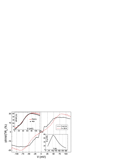
We should note that measured dV/dI(V) characteristics of the investigated compound are asymmetric having larger dV/dI(V) values for the positive bias. The similar asymmetry was also reported in NaidyukBanafeas for the samples with =0.25. In Fig. 6, we present the antisymmetric part of for the PC from Fig. 5. The calculated demonstrates a broad maximum at about 70–80 mV. Qualitatively, the shape of the latter corresponds well to the temperature dependence of the thermopower S(T) measured for the isostructural compound Ba0.7K0.3Fe2As2 Yan (see right inset in Fig. 6). This fact points out to that the PCs at high bias are certainly in the thermal regime while at the low bias the spectral regime is possible. Detail analysis of the thermal regime is given in NaidyukBanafeas for the sample with =0.25.
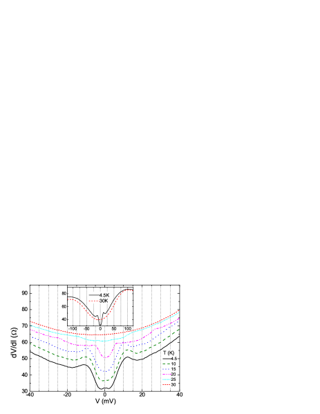
Let’s turn to curves with AR-like shape shown on Fig. 5. Figure 7 presents the temperature measurements of the dV/dI(V) in a wide temperature range. Two curves measured at lowest and highest temperature in a wide voltage range are shown separately in the inset. Like in the case of compounds with =0.25 NaidyukBanafeas , the dV/dI(V) curves possess a pronounced asymmetry and display high-bias maxima (here at about 100 mV). Besides, at the lowest temperatures dV/dI(V) displays zero-bias minima, which are likely due to Andreev reflection. At the temperature rise they transform to a single minimum with the decrease of its amplitude. Finally it vanishes above 25 K, what is close to of the bulk sample for =0.35. Calculation of the SC gap using conventional BTK fit procedure Daghero2011 results in 3.7 meV for this PC and the reduced gap value 2kBT if we take Tc in the range 25–30 K, where the dip minimum in on in Fig. 7 disappears. Remind, that above we paid attention that this PC may be affected by heating with voltage increase and the developed peaks around mV may influence the gap determination.
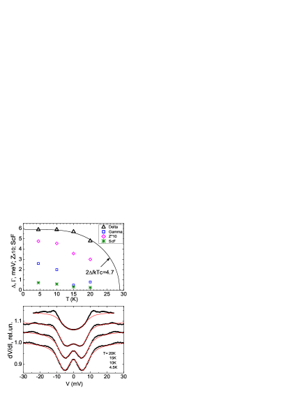
So, we have carried out similar procedure (fit) for a PC () from Fig. 5 with more pronounced AR minima. The results are shown in Fig. 8. For this PC 6 meV is larger and the reduced gap value 2kBT, where Tc is taken from the BCS curve in Fig. 8, because this PC has not survived the temperature increase above 20 K. The reduced gap value estimated from the BTK fit using the local Tc in other PCs results in average to 2kBTc = 3.61. As we mentioned above for the compound with =0.25 the larger value 2k6 was found. So, the difference between these two compounds is that for sample with =0.25 superconductivity coexist with spin-density wave order.
The obtained coupling strength values correspond well to those 2kBTc = 2.5–4 for another hole-doped system from this family Ba0.55K0.45Fe2As2 measured by the same PCAR technique in Szabo . Besides, the lower value of 2kBTc = 2.0–2.6 is extracted for the similar system Ba0.6K0.4Fe2As2 by PC study in XinLu . At the same time, the gap value obtained from ARPES measurements Aswartham for the compound with the highest Tc (=0.4) is maximal (around 10.5 meV) for the inner barrel and minimal (around 3 meV) for the outer barrel, However, as in the case of sample with =0.25, we could not resolve unequivocally the second gap features. Probably, due to short mean free path of electrons caused by strong elastic scattering we measure some averaged gap by PCs or, it is not excluded, merging of small and large gaps. Also scanning tunneling spectroscopy measurements Song carried out on similar compound Sr0.75K0.25Fe2As2 resolved only one gap, which variates by 16% on a 3 nm length scale, with average 2kBTc = 3.6.
IV CONCLUSIONS
PC studies of Josephson effect and Andreev reflection were carried out on the iron-based superconductor Ba1-xNaxFe2As2 with =0.35 and 0.25. We succeed to detect and study the Josephson effect in PCs between Ba1-xNaxFe2As2 crystals and counterelectrodes from Pb, Ta and Nb. Correspondence of the distance between Shapiro steps to the relation 2 and observed critical current dependence on the microwave power (ScS with of Pb) support the presence of the s-wave singlet pairing symmetry in this new superconductor.
Analysis of the measured PC spectra with Andreev-reflection features shows that at small biases the diffusive regime of the current flow realizes, whereas at the further bias increase the transition to the thermal regime in PCs occurs. In the latter case the shape of dV/dI is defined by the specific resistivity of the investigated sample and the noticed asymmetry of the PC spectra is influenced by the thermopower S(T) behavior. In the spectroscopic regime far below it was possible to detect AR-like zero-bias minima in the range (5–15) mV. Applying of the BTK fit gives the reasonable values of 2kBTc = 3.61. The features on which could be due to the manifestation of the second SC gap appeared very seldom and were not reproducible. This do not allow us to make a detailed numeric analysis of the second SC gap.
Acknowledgements
Funding by the National Academy of Sciences of Ukraine under project 3-19 is gratefully acknowledged. Yu.G.N. and O.E.K. would like to thank the IFW Dresden for hospitality and the Alexander von Humboldt Foundation for the financial support in the frame of a research group linkage program. S.W. acknowledges the Deutsche Forschungsgemeinschaft DFG (priority program SPP 1485 and Emmy Nother program; projects BU887/15-1 and WU595/3-2) for support. We thank B. Büchner for valuable discussions.
References
- (1) M. Rotter, M. Tegel, and D. Johrendt, Phys. Rev. Lett. 101, 107006 (2008).
- (2) Kalyan Sasmal, Bing Lv, Bernd Lorenz, Arnold M. Guloy, Feng Chen, Yu-Yi Xue, and Ching-Wu Chu, Phys. Rev. Lett. 101, 107007 (2008).
- (3) A. A. Kordyuk, Fiz. Nizk. Temp., 38, 1119 (2012) [Low Temp. Phys., 38, 888 (2012)],
- (4) P. Seidel, Supercond. Sci. Technol. 24 043001 (2011).
- (5) D. Daghero, M. Tortello, G. A. Ummarino and R. S. Gonnelli1, Rep. Prog. Phys. 74, 124509 (2011).
- (6) I. O. Kulik, I. K. Yanson, Josephson Effect in Superconducting Tunneling Structures, (John Wiley & Sons, Incorporated, 1972).
- (7) A. Barone and G. Paterno, Physics and Applications of the Josephson Effect (New York: Wiley, 1982)
- (8) Xiaohang Zhang, Yoon Seok Oh, Yong Liu, Liqin Yan, Kee Hoon Kim, Richard L. Greene, and Ichiro Takeuchin, Phys. Rev. Lett. 102, 147002 (2009).
- (9) Xiaohang Zhang, Shanta R. Saha, Nicholas P. Butch, Kevin Kirshenbaum, Johnpierre Paglione, Richard L. Greene, Yong Liu, Liqin Yan, Yoon Seok Oh, Kee Hoon Kim and Ichiro Takeuchi, Appl. Phys. Lett. 95, 062510 (2009).
- (10) Takayoshi Katase, Yoshihiro Ishimaru, Akira Tsukamoto, Hidenori Hiramatsu, Toshio Kamiya, Keiichi Tanabe & Hideo Hosono, Nat. Commun. 2, 409 (2011).
- (11) S. Döring, M. Monecke, S. Schmidt, F. Schmidl, V. Tympel, J. Engelmann, F. Kurth, K. Iida, S. Haindl, I. Mönch, B. Holzapfel, and P. Seidel, J. Appl. Phys. 115, 083901 (2014).
- (12) P. Szabó, Z. Pribulová, G. Pristáš, S. L. Bud’ko, P. C. Canfield, and P. Samuely, Phys. Rev. B 79, 012503 (2009).
- (13) Xin Lu, W. K. Park, H. Q. Yuan, G. F. Chen, G. L. Luo, N. L. Wang, A. S. Sefat, M. A. McGuire, R. Jin, B. C. Sales, D. Mandrus, J. Gillett, Suchitra E. Sebastian and L. H. Greene, Supercond. Sci. Technol. 23, 054009 (2010).
- (14) Yu. G. Naidyuk, O. E. Kvitnitskaya, I. K. Yanson, S. Aswartham, G. Fuchs, K. Nenkov, and S. Wurmehl, Phys. Rev. B 89, 104512 (2014).
- (15) S. Aswartham, M. Abdel-Hafiez, D.Bombor, M.Kumar, A.U.B. Wolter, C.Hess, D.V.Evtushinsky,V. B. Zabolotnyy, A. A. Kordyuk, T. K. Kim, S. V. Borisenko, G. Behr, B. Büchner, and S. Wurmehl, Phys.Rev. B 85, 224520 (2012).
- (16) K. K. Likharev, Dynamics of Josephson Junctions and Circuits (Philadelphia, PA: Gordon and Breach, 1986)
- (17) O. P. Balkashin, I. I. Kulik, I. K. Yanson, Yu. G. Litvinenko, V. T. Zagoskin, Fiz. Nizk. Temp. 16, 321 (1990) [Sov. J. Low Temp. Phys, 16, 176 (1988)].
- (18) Yu. G. Naidyuk and I. K. Yanson, Point-Contact Spectroscopy, Springer Series in Solid-State Sciences (Springer Science+Business Media, Inc), vol. 145, 2005.
- (19) L. Wray, D. Qian, D. Hsieh, Y. Xia, L. Li, J. G. Checkelsky, A. Pasupathy, K. K. Gomes, C. V. Parker, A. V. Fedorov, G. F. Chen, J. L. Luo, A. Yazdani, N. P. Ong, N. L. Wang, and M. Z. Hasan, Phys. Rev. B 78, 184508 (2008).
- (20) B. I. Verkin, I. K. Yanson, I. O. Kulik, O.I. Shklyarevski, A.A. Lysykh, Yu. G. Naydyuk, Solid State Commun. 30, 215 (1979).
- (21) I. O. Kulik, Fiz. Nizk. Temp. 18, 440 (1992) [Sov. J. Low Temp. Phys. 18, 302 (1992)].
- (22) Y. J. Yan, X. F. Wang, R. H. Liu, H. Chen, Y. L. Xie, J. J. Ying, and X. H. Chen, Phys. Rev. B 81, 235107 (2010).
- (23) Yu. G. Naidyuk, O. E. Kvitnitskaya, L. V. Tiutrina, I. K. Yanson, G. Behr, G. Fuchs, S.-L. Drechsler, K. Nenkov, and L. Schultz, Phys. Rev. B 84, 094516 (2011).
- (24) Can-Li Song, Yi Yin, Martin Zech, Tess Williams, Michael M. Yee, Gen-Fu Chen, Jian-Lin Luo, Nan-Lin Wang, E. W. Hudson, and Jennifer E. Hoffman, Phys. Rev. B 87, 214519 (2013).