Stacking-dependent energetics and electronic structure of ultrathin polymorphic V2VI3 topological insulator nanofilms
Abstract
Topological insulators represent a paradigm shift in surface physics. The most extensively studied Bi2Se3-type topological insulators exhibit layered structures, wherein neighboring layers are weakly bonded by van der Waals interactions. Using first principles density-functional theory calculations, we investigate the impact of the stacking sequence on the energetics and band structure properties of three polymorphs of Bi2Se3, Bi2Te3, and Sb2Te3. Considering their ultrathin films up to 6 nm as a function of its layer thickness, the overall dispersion of the band structure is found to be insensitive to the stacking sequence, while the band gap is highly sensitive, which may also affect the critical thickness for the onset of the topologically nontrivial phase. Our calculations are consistent with both experimental and theoretical results, where available. We further investigate tribological layer slippage, where we find a relatively low energy barrier between two of the considered structures. Both the stacking-dependent band gap and low slippage energy barriers, suggest that polymorphic stacking modification may offer an alternative route for controlling the properties of this new state of matter.
pacs:
71.20.-b, 73.20.At, 73.43.Nq, 75.70.TjTopological insulators (TIs) have remarkable electronic properties since the role of relativistic interactions {e.g. spin-orbit coupling (SOC)} is fundamentally different from conventional insulators and semiconductors.Bernevig et al. (2006); Hasan and Kane (2010); Moore (2010); Qi and Zhang (2011) TIs combine an insulating band gap in the bulk of the material with conductive surface states that are protected by time-reversal symmetry.Fu and Kane (2007); Hsieh et al. (2008) The topological behavior has been theoretically predicted and experimentally observed in a variety of systems,Yan and Zhang (2012) such as HgTe quantum wells,Bernevig et al. (2006) the Bi2Se3 family of compounds,Zhang et al. (2009); Wang et al. (2011); Chen et al. (2011a); Scanlon et al. (2012) Heusler compounds,Chadov et al. (2010); Lin et al. (2010); Li et al. (2011) pyrochlores,Guo and Franz (2009) Kondo insulators,Dzero et al. (2010) and thallium-based ternary chalcogenides.Eremeev et al. (2011) Besides the fundamental research in condensed matter physics, TIs have great potential to impact multiple areas of application (e.g. electronic, optoelectronic, and spintronic materials, thermoelectric materials, phase-change-memory and catalytic chemistry).Chen et al. (2011b); Kong and Cui (2011)
To effectively explore the surface conductivity of TIs, ultrathin films with a large surface-to-volume ratio provide attractive systems for transport studies, which are highly relevant for electronic device applications.Chen et al. (2011b) For this purpose, the V2VI3 compounds Bi2Se3, Bi2Te3, and Sb2Te3 are a good choice owing to their layered rhombohedral crystal structure with space group R-3m. The structure contains five atomic layers as a basic unit, denoted as a quintuple layer (QL). There is strong chemical bonding within a QL, with weak van der Waals (vdW) interactions between different QLs. V2VI3 compounds can be easily grown as two-dimensional thin films by molecular beam epitaxy.Chen et al. (2011a); Li et al. (2010) The two-dimensional nanostructures of Bi2Se3, Bi2Te3 and Sb2Te3 have been researched both theoretically and experimentally.Wang et al. (2011); Zhang et al. (2010); Liu et al. (2010); Jiang et al. (2012) Their electronic structure depends on the thickness of the film: Above a critical thickness (D), films will transform from a normal insulator (NI) to a TI.Liu et al. (2010) For the Bi2Se3 system, D = 6 QL (about 6 nm),Zhang et al. (2010); Yazyev et al. (2010) while D = 2 or 3 QL (about 2 or 3 nm) for Bi2Te3Wang et al. (2011); Yazyev et al. (2010); Park et al. (2010) and 4 QL (about 4 nm) for Sb2Te3.Jiang et al. (2012) Below the critical thickness, a surface band gap opens, due to hybridization of overlapping surface state wavefunctions.Zhang et al. (2010) Thus, a minimum film thickness is suggested for topological electronic device applications.
Although the critical thicknesses of Bi2Se3, Bi2Te3 and Sb2Te3 have been studied in theory and experiment, the effect of pressure and stress, which are critical factors in real environments, have not been clearly explored.Liu et al. (2011); Young et al. (2011); Zhang et al. (2011). Liu et al. have indicated that uniaxial strain in the 111 direction is an important parameter for influencing the topological insulating phase and the direct band gap of Bi2Se3 at the point.Liu et al. (2010, 2011) However, besides uniaxial strain, shear strain could also be important in applications for ultrathin layered material: such as graphite,Lebedeva et al. (2011) boron nitride,Liu et al. (2003) and V2VI3 compounds. The weak van der Waals force between these layers leads to the possibility of layer slippage and polytypism. When layered materials are used as mechanical components of nano-devices, the properties of friction are extremely important. The nanotribologies of bilayer graphene and boron nitride layers have been intensively researched; the results show that the associated energy barriers are extremely low.Lebedeva et al. (2011); Liu et al. (2003); Popov et al. (2011) The influence of layer sequencing and slippage in V2VI3 TI compounds, which directly relates to their usage in electronic device applications, is the subject of this study.

In these V2VI3 compounds, there are three QLs in each bulk conventional hexagonal unit cell, as shown in Fig. 1. There are also three unique lattice sites (A, B and C). Different polymorphic stacking types are labeled by the group VI atoms in each QL. Thus, the normal structure has a ABC-BCA-CAB stacking sequence, whereas the ABC-CAB-BCA top-like stacking (e.g. A-on-A, C-on-C etc.) is denoted as the top structure and a ABC-ABC-ABC fcc-like stacking will then correspond to the fcc structure. Due to the weak interaction between these QLs and the strong covalent bonding within each QL, when a shear stress is applied perpendicular to the z direction, inter-QLs could easily move or experience a mechanical slip. X-ray diffraction experiments for V2VI3 compounds confirm the existence of the normal structure, while the other polymorphic fcc and top structures have not yet been experimentally determined. However, if formed predominately near/at the surface, alternative polymorphic stacking sequences may not give rise to an appreciable difference in their diffraction patterns.
In this paper, we employ density-functional theory (DFT) calculations (with SOC treated explicitly) to study the effects of polymorphic stacking and planar slippage on the electronic structures and the critical thickness of the polymorphs of V2VI3 (namely, Bi2Se3, Bi2Te3 and Sb2Te3) ultrathin nanofilms as a function of film thickness.
I Methodology and computational approach
All DFT calculations, including geometry relaxation and electronic structure, are performed on the basis of the projector augmented wave methodKresse and Joubert (1999) implemented in the Vienna Ab Initio Simulation Package (VASP) code.Kresse and Furthmüller (1996) The exchange-correlation functional used is the generalized gradient approximation (GGA) due to Perdew, Burke, and Ernzerhof (PBE),Perdew et al. (1996); Scheidemantel et al. (2003) including scalar-relativistic effects in addition to SOC. The latter is known to be of great importance in accounting for the topologically protected surface states in TIs. The kinetic energy cutoff of electron wavefunctions is set to 500 eV and a k-point sampling of 12121 for all films was found to be converged. A vacuum region of 20 Å is used to avoid spurious interactions between repeating slabs. Both the shape and size of the unit cell and the relative atomic positions are relaxed with a force tolerance of 0.01 eV/Å. The dispersion-corrected DFT approach due to Grimme et al. (DFTD2) has been used in which long-range dispersion interactions are empirically described by a pair-potential of the form.Grimme et al. (2010) The Grimme-D2 coefficients are obtained from values tabulated in terms of the chemical identity of the atoms: = 63.565, 38.459, 12.643 and 31.750; = 1.725, 1.710, 1.610 and 1.720 for Bi, Sb, Se and Te atoms, respectively.DFT
In addition, hybrid DFT calculations at the level of HSE06SOC for Bi2Se3 nanofilms have been used to study the electronic band structure. This is because the HSE06 hybrid functional typically presents a considerable improvement over semi-local density-functionals for the description of the band gaps of solid-state systems.Franchini et al. (2005); Krukau et al. (2006) This, in turn, is compared to available results using the van der Waals density functional with Cooper’s exchange (vdW-DF)Luo et al. (2012) and Yazyev et al. (2012) calculations in the literature.
The QL-QL interaction energies of ultrathin nanofilms, from 1 QL to 6 QLs have been calculated using:
| (1) |
where and are the total energy of the system in question and that of 1 QL, respectively, and is the number of QLs in that system. Since the base unit is 1 QL, denotes the relative thermodynamic stability of the ultrathin film stacked per QL. In addition, to investigate the planar slippage energy barriers for these V2VI3 polymorphs, we employ the climbing-image nudged elastic band (CI-NEB) method at the level of PBED2.Henkelman et al. (2000)
II Results and discussion
II.1 Bulk structures of V2VI3 compounds
The crystal structures for three different polymorphic stacking sequences: normal, fcc and top are shown in Fig. 1, with the optimized lattice constants listed in Tab. 1. The DFT+D2 optimized bulk structures are found to be in good agreement with the available experimental resultsWyckoff (1964) and the vdW-DF values,Luo et al. (2012) and are much closer to these results than previously calculated theoretical results (which do not include vdW corrections).Wang and Cagin (2007) This signals that the DFTD2 approach is adequate for describing these weakly-bonded layered systems. Cohesive energies of the bulk V2VI3 polymorphs are calculated and we find that all bulk structures yield a negative value, i.e. stable with respect to their corresponding atomic energies (See Tab. 1). The normal structure is the most favored bulk polymorph, while the top structure is least stable. However, for Bi2Te3 and Sb2Te3 the differences between normal, fcc, and top structures are marginal. Only the normal stacking of Bi2Se3 is notably more stable compared to the other polymorphs. We have calculated the electronic band structures of bulk normal Bi2Se3 with PBESOC and HSESOC. The band gap energy, of bulk Bi2Se3 is calculated to be 0.36 eV for PBESOC and 0.28 eV for HSE06SOC, respectively. Surprisingly, the PBESOC seems to be in a better agreement with other theoretical reports (0.30 eV) and experimental data (0.35 eV) than the slightly underestimated HSE06SOC value.Zhang et al. (2009); Black et al. (1957); Vidal et al. (2011) We note that for Bi2Se3 corrections are known to change the character of the band gap from an indirect to a direct one.Yazyev et al. (2012); Nechaev et al. (2013)
| Bi2Se3 | Bi2Te3 | Sb2Te3 | ||
| normal | 4.092 | 4.349 | 4.195 | |
| fcc | 4.071 | 4.290 | 4.144 | |
| top | 4.057 | 4.282 | 4.142 | |
| Experiment | 4.13811footnotemark: 1 | 4.38311footnotemark: 1 | 4.25011footnotemark: 1 | |
| Theory (normal) | 4.12522footnotemark: 2 | 4.36022footnotemark: 2, 4.53033footnotemark: 3 | 4.44033footnotemark: 3 | |
| normal | 28.91 | 31.09 | 30.81 | |
| fcc | 29.60 | 32.03 | 31.85 | |
| top | 32.15 | 34.74 | 34.53 | |
| Experiment | 28.6411footnotemark: 1 | 30.4911footnotemark: 1 | 30.3511footnotemark: 1 | |
| Theory (normal) | 28.7622footnotemark: 2 | 30.1722footnotemark: 2, 30.6333footnotemark: 3 | 30.2933footnotemark: 3 | |
| normal | 0.36 | 0.15 | 0.13 | |
| Experiment | 0.3544footnotemark: 4 | 0.1755footnotemark: 5,0.1544footnotemark: 4, 0.1366footnotemark: 6 | 0.3044footnotemark: 4, 0.2166footnotemark: 6 | |
| Theory (normal) | 0.3077footnotemark: 7, 0.3188footnotemark: 8 | 0.0888footnotemark: 8, 0.0533footnotemark: 3 | 0.0333footnotemark: 3 | |
| normal | 4.30 | 3.82 | 3.17 | |
| fcc | 4.00 | 3.80 | 3.16 | |
| top | 3.98 | 3.76 | 3.04 |
II.2 Ultrathin V2VI3 nanofilms
II.2.1 Energetics and thermodynamic stability of V2VI3 nanofilms
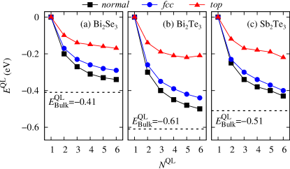
For the nanofilms of these V2VI3 materials, we perform PBED2(SOC) calculations to study their QL-QL interaction energy, , as well as to understand their electronic band properties as a function of increasing number of QLs, . Figure 2 shows the variation of for normal, fcc, and top structured nanofilms as a function of for Bi2Se3 (Fig. 2a), Bi2Te3 (Fig. 2b), and Sb2Te3 (Fig. 2c), respectively. for all three stackings considered in this work are calculated to be negative, and converge to the bulk-like values () with increasing . Taking the bulk-stacked normal structure as an example, we find that , , and eV for Bi2Se3, Bi2Te3, and Sb2Te3, respectively. The top structured nanofilms have the least favorable , while the naturally forming normal structure yield the most favorable , with almost similar values for fcc stacked nanofilms. These results are also consistent with the calculated cohesive energies of their bulk polymorphs, as illustrated above. Given that the calculated average difference in between the normal and fcc polymorphs is only about 0.06 eV, it is not difficult to imagine metastable fcc forming from normal stacked films via a -like (i.e. diffusionless) planar displacement, especially when the film thickness is in the nanometer range.
To study the energetic profile of this possible planar displacement, we use the the simplest 2 QL nanofilms for each V2VI3 to study planar displacement (here, we term this as ). Similar to the slippage in other 2D materials e.g. bilayer graphene and boron nitride,Lebedeva et al. (2011); Liu et al. (2003) the upper QL may slip along the or directions as shown in Fig. 3a. In these two directions, normal, fcc, and top structure will appear when the bottom Se atomic layer in the upper QL is located in B, C and A sites, respectively. Since each QL is one unit, movement appears only between adjoining QLs. To understand the barrier needed to undergo this slippage in the direction, we have also considered possible transition states (TS) structures between the normal and the fcc structured nanofilm. For the other direction, the pathway goes via the top polymorph. These mid-way configurations are consistent with the slippage in bilayer graphene and boron nitride.Sakamoto et al. (2010)
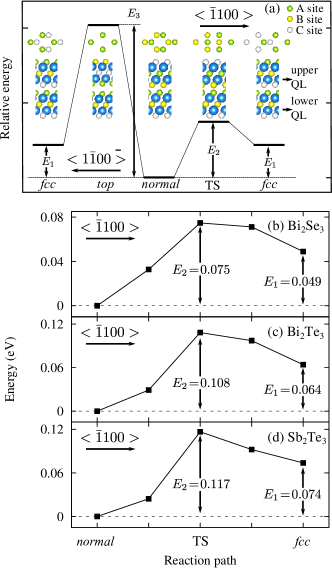
To calculate these slippage energy barriers, the energies of and have been defined in Fig. 3a, where , , , and denote the energies of normal, fcc, and top structure as well as the transition state, respectively. As shown in Figs. 3b to 3d, the energies of top with respect to normal structured films, is calculated to be 0.049, 0.064, and 0.074 eV for Bi2Se3, Bi2Te3, and Sb2Te3, respectively. And based on our CI-NEB calculations, for the energy barrier in the direction, is found to be 0.075, 0.108, and 0.117 eV for Bi2Se3, Bi2Te3, and Sb2Te3, respectively, while for the direction, is found to be 0.205, 0.254, and 0.295 eV, correspondingly. We see that is at least two to three times larger than for all cases. Compared to the reported (19.3 meV) and area-normalized (1.6 meV/Å2) values for bilayer graphene,Lebedeva et al. (2011) we find rather similar orders of magnitude for the V2VI3 chalcogenide nanofilms: 13.8 and 4.8 meV/Å2 for Bi2Se3 films, 18.3 and 5.5 meV/Å2 for Bi2Te3 films, and 16.4 and 6.5 meV/Å2 for Sb2Te3 films, respectively. This would then imply that the martensitic normal-to-fcc slippage would most probably occur for these V2VI3 chalcogenide nanofilms via the rather than the direction.
II.2.2 Electronic structure of V2VI3 nanofilms
Turning to the electronic structure of the normal and fcc stacked nanofilms of V2VI3, we study both the electronic band dispersion, as well as the electron density plots (at the band-edges) to understand how their topological insulating properties might be influenced by both stacking and film thickness in these nanosystems. In Fig. 4, we calculate and plot the electronic band structures (using PBESOC), showing only the highest occupied crystal orbital (HOCO) and the lowest unoccupied crystal orbital (LUCO) for different numbers of QLs. The full band structures are shown in Fig. 7 of the Appendix section, where the number of bands necessarily increases linearly with the thickness of the films. The overall band dispersion profile (especially near the point) of the normal structured films are found to be rather similar to those of the corresponding fcc polymorph, but the clear difference lies in the variation in the magnitude of . To cross-check our PBE+SOC results, we have also selectively calculated the electronic structure of 1 and 2 QL normal and fcc stacking of Bi2Se3 using HSE06+SOC where the predicted are plotted in Fig. 5.
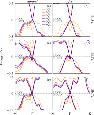
For Bi2Se3, decreases to zero when the of normal structured nanofilms increases to 6, while that of all fcc-like films remain greater than zero. The predicted of Bi2Se3 normal structured films are in good agreement with other theoretical reports,Liu et al. (2010); Yazyev et al. (2010, 2012); Luo et al. (2012) but differ from the reported experimental data for Bi2Se3 films,Zhang et al. (2010) as shown in Fig. 5a. Interestingly, the predicted of the fcc polymorphs, except for the 6 QL nanofilm, seem to agree closely with the experimental of Bi2Se3 films. Accordingly, the predicted of Bi2Se3 fcc structured films are systematically larger than that of the Bi2Se3 normal stacked. Our HSE06+SOC derived for 2 QL normal and fcc structure show the same tendency (albeit having larger absolute values of , and poorer agreement with reported experimental values). The of the fcc structured 6 QL is close to zero (0.02 eV), which may lead to a closure of the band gap when the increases continually. For Bi2Te3, as shown in Fig. 5b, the of the normal polymorph decreases to zero when is increased to 3, again agreeing with other theoretical reports.Liu et al. (2010); Yazyev et al. (2010, 2012); Luo et al. (2012) In contrast to Bi2Se3, the of the fcc structured films quickly reaches zero when reaches 2. For Sb2Te3, of all normal structural films are greater than (or close to) zero for less than 5 while decreases to zero when the of fcc stacked films increases to 4, cf. Fig. 5c. Again, the reported experimental dataJiang et al. (2012) seems to agree better with the predicted of the fcc polymorph.
Based on the above comparison, within the accuracy of PBESOC DFT, the experimentally measured values of for these V2VI3 nanofilms seem to better match those of V2VI3 fcc structured nanofilms, rather than the assumed more stable normal stacking. Although from our bulk calculations of Bi2Se3, we find that the PBESOC value is found to agree better with available experimental and values, we cannot rule out the intrinsic deficiencies of semi-local DFT which could underestimate the predicted values for these polymorphic nanofilms. We also note that a self-consistent relativistic quasiparticle treatment may change the quantitative nature of our results, but the qualitative trends discussed here are expected to be reliable.

Although vanishing values of for some nanofilms are predicted, this is not sufficient information to conclude that these states are topologically protected. For systems with inversion symmetry, such as the V2VI3 compounds considered in this work, the Z2 topological order can be determined by a parity analysis of the occupied states at time-reversal points in the Brillouin zone.Yazyev et al. (2012); Fu and Kane (2007) As a first approximation to this full Z2 topological analysis,Liu et al. (2011) we plot and study the point electron density distributions (namely the HOCO and LUCO states) for a selection of films in Fig. 6.

Taking the normal stacked 5 QL Bi2Se3 as a starting example, the HOCO state is more localized on the more electronegative Se anion, while the electron density of the LUCO is mainly concentrated on the Bi cation, which is typical of a normal insulator. However, upon increasing to 6, the orbital symmetry of the HOCO and LUCO of the normal stacked 6 QL film inverts (as compared to that of 5 QL; see Fig. 6a). The electron density plot of the 6 QL normal structured films LUCO resembles that of the HOCO of the 5 QL film, and vice versa. This inversion of the orbital character suggests a possible transition from a normal insulator (NI) to a TI, which has been observed in experimental measurements.Zhang et al. (2010) However, for the fcc stacked Bi2Se3 films, the calculated HOCO and LUCO plots for ranging from 1 to 6 show very similar orbital character, suggesting that no such NI to TI inversion has taken place. We illustrate this for the 5 and 6 QL fcc structured films in Fig. 6b. For the Bi2Te3 nanofilms, an orbital parity inversion is observed for both stackings normal and fcc, taking place at the increase from 3 QL to 4 QL for the normal structure, cf. Fig. 6c, and for the fcc-like films the inversion is observed when is increased from 2 to 3. And likewise, based on the electron density distribution for Sb2Te3, the orbital parity is predicted to be inverted for both normal and fcc structure (i.e. 4 to 5 QL for normal and 3 to 4 QL for fcc). 1, the critical change from 3 to 4 QL in fcc structured films matches the experimental results better.Jiang et al. (2012) The inversion at a lower number of QLs for the fcc stacking may be due to a reduced overlap of the surface states, since the fcc structured slabs are thicker than the normal stacked, cf. also Table 1.
Upon studying the band gap, , and orbital character inversion as a function of for the normal and fcc structure of these V2VI3 nanofilms, it seems to suggest that given the very low energy barriers for the normal-to-fcc slippage, metastable fcc structured nanofilms of these V2VI3 compounds could well form and offer different electronic band properties (e.g. critical for orbital parity inversion), especially for Bi2Se3 nanofilms. Thus, when these layered V2VI3 nanofilms are used in nano-devices, due to the weak interaction between these QLs, a mechanical slip could easily be experienced and thus the desired topological insulating character of these films could be intentionally exploited for new technologies.
III Conclusion and summary
The energetics of stacking sequences and their effect on the transition from normal to topological insulating behavior in Bi2Se3, Bi2Te3 and Sb2Te3 nanofilms have been investigated via first-principles DFT calculations. We find that the overall band dispersion is relatively insensitive to the stacking sequence, while the magnitude of the band gap, and the critical thickness for a band edge parity inversion, is more sensitive. Relatively low energy barriers may allow for martensitic normal-to-fcc slippage, which are predicted to change the electronic structure and alter the topological behavior of these V2VI3 nanofilms. Thus, the effect of mechanical shear stress should be carefully considered in applications of topological insulators, e.g. the nanotribological conversion from TI to NI may be exploited in nano-circuit switches. In this context, a more detailed experimental analysis of the present and accessible stacking sequences is called for.
Acknowledgements.
The authors gratefully acknowledge support by the Global Frontier R & D Program (2013M3A6B1078881) on Center for Global Frontier Hybrid Interface Materials (GFHIM) funded by the Korean Ministry of Science, ICT & Future Planning, as well as the Australian Research Council (ARC). This work was also supported by the third Stage of Brain Korea 21 Plus Project Division of Creative Materials. Computational resources have been provided by the Australian National Computational Infrastructure (NCI) and by the KISTI supercomputing center (KSC-2013-C3-040). A. W. and B. Y. acknowledge support from the Royal Society University Research Fellowship scheme, and the European Research Council Advanced Grant (ERC 291472), respectively.*
Appendix A Supporting Information

| normal | fcc | Experiment | Theory | ||
|---|---|---|---|---|---|
| 1 | 0.86 (1.19) | 0.86 (1.19) | 0.9522footnotemark: 2, 0.7233footnotemark: 3, 0.7333footnotemark: 3, 0.7155footnotemark: 5 | ||
| 2 | 0.15 (0.36) | 0.26 (0.48) | 0.2511footnotemark: 1 | 0.3522footnotemark: 2, 0.1233footnotemark: 3, 0.1144footnotemark: 4, 0.09855footnotemark: 5 | |
| Bi2Se3 | 3 | 0.04 | 0.13 | 0.1411footnotemark: 1 | 0.2122footnotemark: 2, 0.0233footnotemark: 3, 0.0244footnotemark: 4, 0.00455footnotemark: 5 |
| 4 | 0.01 | 0.07 | 0.0711footnotemark: 1 | 0.1122footnotemark: 2, 0.0133footnotemark: 3, 0.0344footnotemark: 4, 0.0155footnotemark: 5 | |
| 5 | 0.01 | 0.04 | 0.0411footnotemark: 1 | 0.0822footnotemark: 2, 0.0033footnotemark: 3 | |
| 6 | 0.00 | 0.02 | 0.0011footnotemark: 1 | ||
| 1 | 0.34 | 0.34 | 0.6322footnotemark: 2, 0.4033footnotemark: 3, 0.3444footnotemark: 4, 0.3955footnotemark: 5 | ||
| 2 | 0.14 | 0.00 | 0.0722footnotemark: 2, 0.1133footnotemark: 3, 0.1444footnotemark: 4, 0.1555footnotemark: 5 | ||
| Bi2Te3 | 3 | 0.00 | 0.00 | 0.0222footnotemark: 2, 0.0233footnotemark: 3, 0.0544footnotemark: 4, 0.0455footnotemark: 5 | |
| 4 | 0.00 | 0.00 | 0.0122footnotemark: 2, 0.0133footnotemark: 3, 0.0244footnotemark: 4, 0.00555footnotemark: 5 | ||
| 5 | 0.00 | 0.00 | 0.0122footnotemark: 2, 0.0033footnotemark: 3, 0.0044footnotemark: 4 | ||
| 6 | 0.00 | 0.00 | 0.00122footnotemark: 2, 0.0033footnotemark: 3 | ||
| 1 | 0.73 | 0.73 | 0.6766footnotemark: 6 | ||
| 2 | 0.10 | 0.19 | 0.2666footnotemark: 6 | ||
| Sb2Te3 | 3 | 0.01 | 0.06 | 0.0666footnotemark: 6 | |
| 4 | 0.03 | 0.00 | 0.0066footnotemark: 6 | ||
| 5 | 0.00 | 0.00 | |||
| 6 | 0.00 | 0.00 |
References
- Bernevig et al. (2006) B. A. Bernevig, T. L. Hughes, and S.-C. Zhang, Science 314, 1757 (2006).
- Hasan and Kane (2010) M. Z. Hasan and C. L. Kane, Rev. Mod. Phys. 82, 3045 (2010).
- Moore (2010) J. E. Moore, Nature 464, 194 (2010).
- Qi and Zhang (2011) X.-L. Qi and S.-C. Zhang, Rev. Mod. Phys. 83, 1057 (2011).
- Fu and Kane (2007) L. Fu and C. L. Kane, Phys. Rev. B 76, 045302 (2007).
- Hsieh et al. (2008) D. Hsieh, D. Qian, L. Wray, Y. Xia, Y. S. Hor, R. J. Cava, and M. Z. Hasan, Nature 452 (2008).
- Yan and Zhang (2012) B. Yan and S.-C. Zhang, Rep. Prog. Phys. 75, 096501 (2012).
- Zhang et al. (2009) H. Zhang, C.-X. Liu, X.-L. Qi, X. Dai, Z. Fang, and S.-C. Zhang, Nat. Phys. 5, 438 (2009).
- Wang et al. (2011) G. Wang, X.-G. Zhu, Y.-Y. Sun, Y.-Y. Li, T. Zhang, J. Wen, X. Chen, K. He, L.-L. Wang, X.-C. Ma, J.-F. Jia, S. B. Zhang, and Q.-K. Xue, Adv. Mater. 23, 2929 (2011).
- Chen et al. (2011a) X. Chen, X.-C. Ma, K. He, J.-F. Jia, and Q.-K. Xue, Adv. Mater. 23, 1162 (2011a).
- Scanlon et al. (2012) D. O. Scanlon, P. D. C. King, R. P. Singh, A. de la Torre, S. McKeown Walker, G. Balakrishnan, F. Baumberger, and C. R. A. Catlow, Adv. Mater. 24, 2154 (2012).
- Chadov et al. (2010) S. Chadov, X. Qi, J. Kübler, G. H. Fecher, and C. Felser, Nat. Mater. 9, 541 (2010).
- Lin et al. (2010) H. Lin, L. A. Wray, Y. Xia, S. Xu, S. Jia, R. J. Cava, A. Bansil, and M. Z. Hasan, Nat. Mater. 9, 546 (2010).
- Li et al. (2011) C. Li, J. S. Lian, and Q. Jiang, Phys. Rev. B 83, 235125 (2011).
- Guo and Franz (2009) H.-M. Guo and M. Franz, Phys. Rev. Lett. 103, 206805 (2009).
- Dzero et al. (2010) M. Dzero, K. Sun, V. Galitski, and P. Coleman, Phys. Rev. Lett. 104, 106408 (2010).
- Eremeev et al. (2011) S. V. Eremeev, G. Bihlmayer, M. Vergniory, Y. M. Koroteev, T. V. Menshchikova, J. Henk, A. Ernst, and E. V. Chulkov, Phys. Rev. B 83, 205129 (2011).
- Chen et al. (2011b) H. Chen, W. Zhu, D. Xiao, and Z. Zhang, Phys. Rev. Lett. 107, 056804 (2011b).
- Kong and Cui (2011) D. Kong and Y. Cui, Nat. Chem. 3, 845 (2011).
- Li et al. (2010) Y.-Y. Li, G. Wang, X.-G. Zhu, M.-H. Liu, C. Ye, X. Chen, Y.-Y. Wang, K. He, L.-L. Wang, X.-C. Ma, H.-J. Zhang, X. Dai, Z. Fang, X.-C. Xie, Y. Liu, X.-L. Qi, J.-F. Jia, S.-C. Zhang, and Q.-K. Xue, Adv. Mater. 22, 4002 (2010).
- Zhang et al. (2010) Y. Zhang, K. He, C.-Z. Chang, C.-L. Song, L.-L. Wang, X. Chen, J.-F. Jia, Z. Fang, X. Dai, W.-Y. Shan, S.-Q. Shen, Q. Niu, X.-L. Qi, S.-C. Zhang, X.-C. Ma, and Q.-K. Xue, Nat. Phys. 6, 584 (2010).
- Liu et al. (2010) C.-X. Liu, H. Zhang, B. Yan, X.-L. Qi, T. Frauenheim, X. Dai, Z. Fang, and S.-C. Zhang, Phys. Rev. B 81, 041307 (2010).
- Jiang et al. (2012) Y. Jiang, Y. Wang, M. Chen, Z. Li, C. Song, K. He, L. Wang, X. Chen, X. Ma, and Q.-K. Xue, Phys. Rev. Lett. 108, 016401 (2012).
- Yazyev et al. (2010) O. V. Yazyev, J. E. Moore, and S. G. Louie, Phys. Rev. Lett. 105, 266806 (2010).
- Park et al. (2010) K. Park, J. J. Heremans, V. W. Scarola, and D. Minic, Phys. Rev. Lett. 105, 186801 (2010).
- Liu et al. (2011) W. Liu, X. Peng, C. Tang, L. Sun, K. Zhang, and J. Zhong, Phys. Rev. B 84, 245105 (2011).
- Young et al. (2011) S. M. Young, S. Chowdhury, E. J. Walter, E. J. Mele, C. L. Kane, and A. M. Rappe, Phys. Rev. B 84, 085106 (2011).
- Zhang et al. (2011) J. L. Zhang, S. J. Zhang, H. M. Weng, W. Zhang, L. X. Yang, Q. Q. Liu, S. M. Feng, X. C. Wang, R. C. Yu, L. Z. Cao, L. Wang, W. G. Yang, H. Z. Liu, W. Y. Zhao, S. C. Zhang, X. Dai, Z. Fang, and C. Q. Jin, P. Natl. Acad. Sci. USA 108, 24 (2011).
- Lebedeva et al. (2011) I. V. Lebedeva, A. A. Knizhnik, A. M. Popov, Y. E. Lozovik, and B. V. Potapkin, Phys. Chem. Chem. Phys. 13, 5687 (2011).
- Liu et al. (2003) L. Liu, Y. P. Feng, and Z. X. Shen, Phys. Rev. B 68, 104102 (2003).
- Popov et al. (2011) A. M. Popov, I. V. Lebedeva, A. A. Knizhnik, Y. E. Lozovik, and B. V. Potapkin, Phys. Rev. B 84, 045404 (2011).
- Kresse and Joubert (1999) G. Kresse and D. Joubert, Phys. Rev. B 59, 1758 (1999).
- Kresse and Furthmüller (1996) G. Kresse and J. Furthmüller, Phys. Rev. B 54, 11169 (1996).
- Perdew et al. (1996) J. P. Perdew, K. Burke, and M. Ernzerhof, Phys. Rev. Lett. 77, 3865 (1996).
- Scheidemantel et al. (2003) T. J. Scheidemantel, C. Ambrosch-Draxl, T. Thonhauser, J. V. Badding, and J. O. Sofo, Phys. Rev. B 68, 125210 (2003).
- Grimme et al. (2010) S. Grimme, J. Antony, S. Ehrlich, and H. Krieg, J. Chem. Phys. 132, 154104 (2010).
- (37) Grimme’s DFT-D3 program, URL: http://toc.uni-muenster.de/DFTD3.
- Franchini et al. (2005) C. Franchini, V. Bayer, and R. Podloucky, Phys. Rev. B 72, 045132 (2005).
- Krukau et al. (2006) A. V. Krukau, O. A. Vydrov, A. F. Izmaylov, and G. E. Scuseria, J. Chem. Phys. 125, 224106 (2006).
- Luo et al. (2012) X. Luo, M. B. Sullivan, and S. Y. Quek, Phys. Rev. B 86, 184111 (2012).
- Yazyev et al. (2012) O. V. Yazyev, E. Kioupakis, J. E. Moore, and S. G. Louie, Phys. Rev. B 85, 161101 (2012).
- Henkelman et al. (2000) G. Henkelman, B. P. Uberuaga, and H. Jónsson, J. Chem. Phys. 113, 9901 (2000).
- Wyckoff (1964) R. W. G. Wyckoff, ed., Crystal Structures Volume 2 (New York: Wiley, 1964).
- Wang and Cagin (2007) G. Wang and T. Cagin, Phys. Rev. B 76, 075201 (2007).
- Black et al. (1957) J. Black, E. M. Conwell, L. Seigle, and C. W. Spencer, J. Phys. Chem. Solids 2, 240 (1957).
- Vidal et al. (2011) J. Vidal, X. Zhang, L. Yu, J.-W. Luo, and A. Zunger, Phys. Rev. B 84, 041109 (2011).
- Nechaev et al. (2013) I. A. Nechaev, R. C. Hatch, M. Bianchi, D. Guan, C. Friedrich, I. Aguilera, J. L. Mi, B. B. Iversen, S. Bl gel, P. Hofmann, and E. V. Chulkov, Physical Review B 87, 121111 (2013).
- Chen et al. (2009) Y. L. Chen, J. G. Analytis, J.-H. Chu, Z. K. Liu, S.-K. Mo, X. L. Qi, H. J. Zhang, D. H. Lu, X. Dai, Z. Fang, S. C. Zhang, I. R. Fisher, Z. Hussain, and Z.-X. Shen, Science 325, 178 (2009).
- Sehr and Testardi (1962) R. Sehr and L. R. Testardi, J. Phys. Chem. Solids 23, 1219 (1962).
- Sakamoto et al. (2010) Y. Sakamoto, T. Hirahara, H. Miyazaki, S.-i. Kimura, and S. Hasegawa, Phys. Rev. B 81, 165432 (2010).