Current flow in biased bilayer graphene: the role of sublattices
Abstract
We investigate here how the current flows over a bilayer graphene in the presence of an external electric field perpendicularly applied (biased bilayer). Charge density polarization between layers in these systems is known to create a layer pseudospin, which can be manipulated by the electric field. Our results show that current does not necessarily flow over regions of the system with higher charge density. Charge can be predominantly concentrated over one layer, while current flows over the other layer. We find that this phenomenon occurs when the charge density becomes highly concentrated over only one of the sublattices, as the electric field breaks layer and sublattice symmetries for a Bernal-stacked bilayer. For bilayer nanoribbons, the situation is even more complex, with a competition between edge and bulk effects for the definition of the current flow. We show that, in spite of not flowing trough the layer where charge is polarized to, the current in these systems also defines a controllable layer pseudospin.
pacs:
73.63.-b,81.05.ueI Introduction
For electronic devices of reduced dimensions, the spatial mapping of charge current is of paramount importance. In a quantum point contact, for example, electrons flow through narrow branching channels rather than the expected uniform propagationTopinka et al. (2000, 2001); these measurements are crucial to understand how the geometry and impurities of the device affect its performance. Graphene, due to its exceptional electronic properties, has been pointed out to have great potential to replace existing materials in traditional electronics A. H. Castro Neto et al. (2009), as well as to be used in new pseudospintronic devicesRycerz et al. (2007); San-Jose et al. (2009); Akhmerov and Beenakker (2007); Gunlycke and White (2011); Schwierz (2010); Pesin and MacDonald (2012). Common to these traditional and new applications, local aspects of charge flow in graphene have to be understood. Studies on zigzag graphene nanoribbons have shown, for low energies, dispersionless and sublattice polarized edge statesCastro et al. (2008). Notably the overlap of these no current-carrying states from opposite edges creates charge flow through the centre of the nanoribbonZârbo and Nikolić (2007). This charge-current asymmetry has been ignored for bilayer graphene (BLG), which offers better options for digital electronics.
A remarkable property of BLG -which potentiates its use in future graphene based electronics- is the possibility of opening and controlling a band gap with a potential difference applied between top and bottom layers (biased bilayer) McCann (2006); Castro et al. (2007); Schwierz (2010); Xu et al. (2013); Ohta et al. (2006); Nilsson et al. (2008); McCann and Koshino (2013). The externally applied perpendicular electric field breaks the inversion symmetry of the system Zhang et al. (2009) allowing to define a layer pseudospin, at least for energies below the interlayer coupling energy Pesin and MacDonald (2012); Abedinpour et al. (2007); San-Jose et al. (2009). Therefore, many devices based on these systems have been proposed recently, which involve the ability to control this layer pseudospin (the charge density polarization between layers induced by the bias) for different bias layoutsMiyazaki et al. (2010); Xia et al. (2010); J. et al. (2012), such as the creation of electron highways Qiao et al. (2011) or pseudospin-valve devices Rycerz et al. (2007); San-Jose et al. (2009); Li et al. (2010). Experimentally, charge localization over different layers and different sublattices due to a bias voltage has been observed in these systems by STM imagesKim et al. (2013), indicating the possibility of controlling layer and sublattice pseudospins in real samples. Even though all the attention that has been given to the possibilities of controlling charge densities in BLG through the bias, the charge flow has been neglected.
The purpose of this paper is to analyze and quantify the main transport features of pristine biased BLG. In particular we are enticed to unveil the relation between charge density and charge flow. Although charge and current are intimately linked by the continuity equation, when the electric field localizes charge over different sublattices in different layers, it is not evident how current density is distributed. Using the lattice Green’s functions we are able to map charge density over each sublattice site in both layers, conjointly with the current flowing towards its neighbors. Our results show that current does not necessarily flow in the regions with higher charge density, and this would have a fundamental role when devising electronics. At low energies, for bulk biased BLG, we observe that charge is primarily concentrated over one layer while current flows over the other layer. We show that this is a consequence of an important concentration of charge in only one of the sublattices in the layer with more charge density. This picture is enriched in biased BLG nanoribbon with zigzag edges where additional sublattice polarized edge states Nakada et al. (1996); Lima et al. (2010); Lv and Li (2012); Wang et al. (2011) compete with bulk sublattice polarization. The distribution of the current for edge states is found to also depend whether the most external atom of the edge corresponds to a coupled or uncoupled sublattice in the AB stacking. We show results as a function of energy around Fermi energy, and also as a function of nanoribbon width and bias strength (), elucidating the behavior of current flow and the main role of sublattices. The effects of disorder and next-nearest neighbor hoppings are also discussed.
II Model
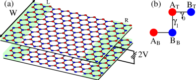
We consider a BLG nanorribon with zigzag edges and Bernal AB stacking, as shown in Fig. 1(a). The width is defined by the number of sites in the transversal direction and Å is the lattice constant for graphene. The infinite BLG zigzag nanoribbon is modelled by the tight binding Hamiltonian:
| (1) |
Here, the first term refers to individual graphene layer (top and bottom), the second term describes the interlayer coupling, and the last two terms introduce the interlayer bias which induces an energy difference between layers parameterized by . Field operators (), () create (annihilate) one electron in sublattice A or B i-th site of the top () or bottom () layer. We use the intralayer nearest-neighbor hopping eV and the interlayer coupling = 0.381 eV Kuzmenko et al. (2009). From our Hamiltonian eq. (1) the Bernal AB stacking is easily recognised, as shown in Fig. 1(b), sublattice sites A in the top layer () are on top of sublattice sites B in the bottom layer (). We refer to this coupled() sites as dimer sites while non-coupled sites ( or ) are non-dimer sites Castro et al. (2008); McCann and Koshino (2013). The Introduction of next-nearest neighbor hopping in each layer and further interlayer couplings, as well as of on site disorder, is discussed in section VI.
To account for the electronic transport properties, the infinite BLG zigzag nanoribbon is divided in three regions; a finite central region and two semi-infinite ribbons acting as contacts Datta (1999). Although eq. (1) describes the dynamics of electrons in the three regions and no qualitative differences can be found among them; it is mandatory to have a finite central region to calculate its Green’s function Datta (1999); Ferry and Goodnick (1999); Lewenkopf and Mucciolo (2013) in order to extract conductance, local density of states (LDOS) (), charge density () and current density ()Bahamon et al. (2011). Despite the fact the transport properties are calculated for the central region, these can be extended to the whole BLG zigzag nanoribbon. The retarded Green’s function is calculated as where is the Hamiltonian of the central region and is the left (right) contact self-energy Datta (1999).
Charge and current are intimately related through the continuity equation, its lattice version can be written as where is the bond charge current operator. results, exactly as one would expect, from the difference of electrons flow in opposite directions. The connection with the Green’s function arises because the quantum statistical average of the bond charge current operator of the form are related to the lesser Green’s function Haug (2008); Datta (1999), in steady state the bond charge current including spin degeneracy is:
| (2) |
=2e/h = 77.48092 A/eV is the natural unit of bond charge current density. The lesser Green’s function in the absence of interactions can be resolved exactly as where is the left (right) contact broadening function and is the Fermi distribution of the left (right) contact. is the hopping parameter between sites and , in our BLG zigzag nanorribon represents for intralayer bond current and for interlayer bond current. In order to quantify the electron flow in a layer we defined the layer current density as:
| (3) |
represents a site in the central region of the nanoribbon in layer ; is the total current at site calculated adding the bond current (eq. (2)) between site and its neighboring sites . Once again, since we are working on a pristine nanoribbon the current density in any slide of our device is exactly the same, because of that we associated it to a layer current density in eq. (3).
Complementary to current density, charge density at site can also be expressed using the lesser Green’s function as:
| (4) |
At equilibrium, all states are occupied as specified by the Fermi-Dirac distribution () and the lesser Green’s function acquires the simple form . Where is the spectral function, which is related to the LDOS as Datta (1999). It is noteworthy that at low bias and low temperature , and clearly it is observed that charge density () has the same local distribution of LDOS (). Given we are interested in how charge and current distributions are related; with no loss of generality, to keep explanations and figures as simples as possible, we will refer from now on to LDOS as charge distribution. To quantify and visualize how charge (LDOS) is distributed over one layer it is defined the charge density per layer as:
| (5) |
III Results for Charge and current density
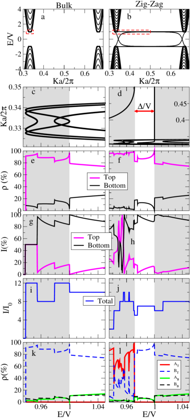
In Fig. 2 we show the band structure and details of the charge and the current densities for BLG under the influence of an applied voltage difference of eV between the two layers. The right column shows the results for a BLG nanoribbon with zigzag edges and width of atoms, while the results at the left column are for a bulk BLG (for which the same width of atoms was considered with periodical boundary conditions).
III.1 Band Structures
The band structure for the bulk BLG in Fig. 2(a) evidences the opening of the energy gap of approximately 2V (observe that the energy scale is normalized by the bias voltage V). The presence of the zigzag edges introduces edge states in the gap region of the band structure, as observed in Fig. 2(b). Zooms into the band structure’s regions marked by the dashed lines in Fig. 2(a) and (b) are shown in Fig. 2(c) and (d), respectively. For the bulk, we see in Fig. 2(c) the well-known “Mexican-hat” structure, due to the applied bias, mixed to other higher bands for this system size and bias (the wider the nanoribbon considered the higher is the density of bands and the band mixing in this region). For the zigzag case, one can see in more detail in Fig. 2(d) that in addition to the usual band structure this region contains two edge states energy bands: a flat band at and a dispersive band for , in agreement with previous works Castro et al. (2008, 2010); Yao et al. (2009); Li et al. (2010); Rhim and Moon (2008). The minimum separation between the edge states bands is =2V (this expression is derived from the difference between dispersive band and flat band Castro et al. (2008) at ). Observe that increases linearly with the external bias V and does not depend on the nanoribbon width.
III.2 Charge and Current Density in each Layer
In Fig. 2(e) and (f) we show the percentage of the total charge density of the bilayer which is accumulated in each of the layers (top or bottom) - once charge in each layer is obtained from eq. (5), its proportion with respect to the total charge in both layers is calculated . Both for the system with zigzag edges and for the bulk there is a clear unbalance between layers, with electronic charge density being concentrated predominantly (from 75 to 100) over the top layer for the entire energy range shown.
The percentage of the current density over each layer is calculated in the same way from eq. (3) and the results are shown in Fig. 2(g) and (h), for bulk and zigzag, respectively. Comparing charge and current densities in each layer, one can see that although the charge densities are highly concentrated over the top layer, the current densities are higher on the bottom layer for a wide energy range, both for bulk or zigzag BLG. This behavior is counterintuitive and contradicts the most basic theoretical model of charge flow.
Fig. 2(i) and (j) show the total current density ( divided by ), which corresponds to the summation of the currents in the top and the bottom layers. The total current density is directly proportional to the conductance of the system.
III.3 The Role of the Sublattices
To investigate the origin of the discrepancy between the charge density and current density in each layer, we compute separately the contribution of each sublattice to the charge density, as shown in Fig. 2(k) and (l). This gives us an important clue to understand the phenomenon: the charge is not only predominantly over one layer (the top layer), there is also a sublattice polarization in this layer.
For the bulk, Fig. 2(k), we observe that the charge on the top layer is entirely over the sublattice , while sublattice shows zero contribution to the charge density in the entire energy range shown. This effect comes from the sublattice asymmetry introduced by the AB-stacking in BLGCastro et al. (2010): the dimer sites ( and ) hybridized their orbitals to form higher energy bands, being the charge density for low energy states located mostly on non-dimer sites ( and ) McCann (2006); Koshino and Ando (2006). Here we show in Fig. 2(k) how this sublattice asymmetry is preserved in the top layer after the application of the voltage difference between the layers. We see that although the charge on top layer keeps completely located over only one sublattice ( non-dimer ), the charge density over the bottom layer is mostly sublattice unpolarized, ie, equally shared between the two sublattices. This interesting characteristic of these systems, which has already been point out in previous experimentalKim et al. (2013), analyticalMcCann and Koshino (2013); Castro et al. (2010) and numericalRamasubramaniam et al. (2011) works, can possibly explain why the current goes preferentially over the bottom layer.
For the zigzag nanoribbon, the density distribution in each sublattice becomes even more interesting, Fig. 2(l), with a clear competition between the bulk effect in the AB-stacking just described and the additional sublattice polarization that is well known to occur around the zigzag edges Castro et al. (2008), as we will show. For energies , we see from Fig. 2(l) that the sublattice distribution is similar to that described to the bulk, with charge on top layer only over sublattice. However, for energies , while Fig. 2(f) tells us that the charge is still over the top layer (more than ), Fig. 2(l) shows that there is an inversion in the subltattice: sublattice is now predominant, with some oscillations. Comparing to the band structure in Fig. 2(d), we see that in this region the dispersive edge-state band plays an important role. The energy split of size corresponds in fact to the split of states localized on opposite edges of the top layer. The states from the flat band at are located on the edge of the top layer where the outermost atoms are atomic sites, the same sublattice that is privileged by the AB-stacking. On the other hand, as in zigzag graphene nanoribbons the outermost atoms in opposite edges belong to different sublattices, the states from the dispersive band at are located on the edge where the outermost atoms of the top layer are sites. And here is where the competition between edge and bulk arises, leading to the oscillations between sublattices observed, with an advantage to the sites, i.e., the edge state localization effect being more robust than the bulk effect.
IV Mapping the Spatial Distribution of Charge and Current over the BLG
In a lattice, we can imagine one electron injected from the left contact hopping from site to site until reaching the right contact. Clearly one electron is enabled to hop on its nearest neighbor if there are electronic states available there; in this regard the spatial distribution of charge and current densities are expected to be related to each other.
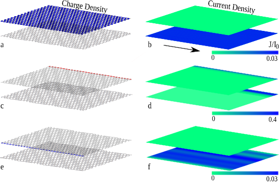
In the discussion of the previous section we have already identified that the polarization of the charge density to only one of the sublattices plays an important role in the discrepancies observed between charge and current densities in each layer. Here, Fig. 3 helps us to observe in more detail the spatial distribution of charge and current densities over each layer (and each sublattice) of the bilayer systems. The systems considered in this calculation of Fig. 3 are exactly the same from Fig. 2: biased BLG of 300 carbon atoms in width, with periodical boundary conditions for the bulk and zigzag edges for the nanoribbon, V=0.07eV. For the representations of the spatial distribution of the charge density, the density on each atomic site is shown here as proportional to the radius of the disk and its color stands for sublattice: red for and and blue for and (same color scheme shown in Fig. 1(b)).
Initially, in Fig. 3(a) and (b) we map charge and current spatial density for a bulk BLG, avoiding in this case any complication introduced by the edge states. This distribution corresponds to the energy - at this energy, Fig2(e) tells us that 80% of the charge is located on top layer, while Fig.2(g) shows that current density is much higher in bottom layer and nearly zero on top layer. Fig. 3(a) shows that on the top layer charge is completely located on non-dimer sites, being homogeneously distributed over the layer. On the bottom layer, although it is not appreciated in Fig. 3(a) because is approximately 10 times smaller than ; there is a homogeneous charge density on and sites (9% each, see Fig. 2(k)). When current density is calculated, as shown in Fig. 3(b), it is appreciated that current is homogeneously distributed over bottom layer while is nearly zero over top layer. This can be understood on account of charge is completely localized on non-dimer sites (). Electrons on these sites can not jump on its nearest neighbors, causing no electron flow over top layer. On the bottom layer, in spite of , charge is homogeneously distributed over both sublattices, allowing electron hopping among sites.
For the BLG zigzag nanoribbons, bias lifts edge states degeneracy. We see from Fig. 3(c) and (e) that the charge densities for energies corresponding to the split edge state bands, and , are highly localized on opposite zigzag edges of the top layer, in agreement to previous calculations Castro et al. (2010); Yao et al. (2009); Rhim and Moon (2008); Li et al. (2010). For the first energy one can see from Fig. 2(l) that nearly 80% of the charge density is located on dimer sites while 18% of the charge is located on non-dimer sites . Spatial mapping of the charge density reveals in Fig. 3(c) an edge state located on only one of the edges of the top layer: the edge whose outermost atoms are from sublattice . Once again due to the considerable difference between the densities in the two sublattices, only the edge state is appreciable. However, charge density is also homogeneously distributed on non-dimer sites () of the top layer. Overlapping of the exponentially decaying edge state () and the homogeneously distributed state () creates a high current density on this edge of the top layer, as depicted on Fig. 3(d). This figure also shows a high current density on the bottom layer right bellow this edge, its origin is similar to the top layer current: this edge at bottom layer terminates at a non-dimer sites sustaining edge states while dimer sites have an enhanced charge density caused by the top layer edge state; these two states overlap creating the highly charge current observed. When next to nearest neighbors are included in monolayer zigzag nanoribbon edge states acquire velocity, this however does not affect charge or current density.
The effect of the sublattice symmetry breaking is also observed for . At this energy, edge states localize on the other edge, the one whose outermost atoms are from sublattice, as shown in Fig. 3(e). Considering that this sublattice corresponds to non-dimer atoms, current on bottom layer is not affected for this energy, as shown in Fig. 3(f): current is distributed over the whole layer. Over the top layer there is no current because charge is completely localized on sites, this situation is reminiscent of bulk biased BLG.
V Current dependence on bias voltage and size
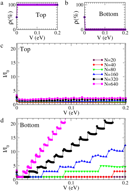
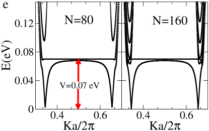
In this section we focus on the effects of the bias voltage strength and the width of the nanoribbons on the current and charge densities. For this purpose, we need first to choose a fixed energy. The experimental observation of a current density highly localized on one of the edges of a BLG nanoribbon, like the current shown in Fig. 3(d), would require an extremely clean sample, as edge disorder would scatter electrons, degrading the current and destroying its spatial localization Mucciolo et al. (2009); Cresti and Roche (2009); Mucciolo and Lewenkopf (2010). On the other hand, setting for a BLG nanorribon offers control of the layer pseudospin: the layer in which charge current is conducted (top or bottom), in a similar way observed for bulk systems (as observed for the current in Figs. 2 and 3) and avoiding the edge disorder sensitivity. Therefore, we choose to investigate here how the current and the charge densities vary with system size and with bias voltage at energy : results are shown in Fig. 4. Figures 4(a) and (b) show that for wider nanoribbons, bias voltage variation and ribbon width do not modify the complete charge density polarization on the top layer. As we have seen, for this energy, charge mostly localizes on non-dimer sites of top layer reducing nearly to zero the current density over top layer. Here we show in Figs. 4(c) that this characteristic is maintained with increasing bias and system sizes. Fig. 4(d) shows a different evolution for the current density on the bottom layer: for wider nanoribbons or larger bias voltages, the current density rises in steps. This dependence is understood from the band structure of the biased BLG nanoribbon, as seen in Fig. 4(e) for eV and widths corresponding to and . It is appreciated that flat bands are fixed at and do not depend on the nanoribbon width. On the other hand, the number of dispersive bands around increases with N, adding more conducting channels. For that reason current density evolves in a plateau-like structure. The peaks observed, at the beginning of each plateau, for wider nanoribbons and are created by the “Mexican-hat” structure of bands crossing .
VI EFFECTS OF DISORDER AND NEXT-NEAREST HOPPINGS
In this section we discuss how disorder and next-nearest neighbor hoppings affect the picture presented in the previous sections. Mainly, we show here that although there are important features introduced by disorder and by further hoppings in the model, the assymmetry between charge and current density distributions is still present, therefore, the effects previously discussed are robust.
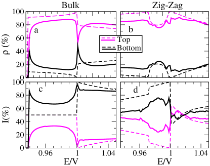
In Fig. 5 we show the comparison between a non-disorderd BLG (dashed lines) and a disordered system (solid lines), again analysing both for a bulk and for a zig-zag nanoribbon. Each layer of these systems here have width of N = 80 atoms and 40 atoms in the length between the contacts. To account for disorder, we introduce a Gaussian-correlated on-site disorder for each layerPereira and Schulz (2008), with site energies ramdomly sorted in a range of width and correlation length for bottom layer and for top layer (). Larger correlation length for the top layer is due to its higher distance from the substrate. For the charge density distribution, Fig. 5(a) and (b), we see that the disorder does not alter significantly the clear concentration of the charge on the top layer for all the energy range shown (except for the bulk at energy exactly E/V=1). For the current density, one can see that, for the bulk, Fig. 5(c), disorder not only does not alter the fact that about 80% of the current goes through bottom layer for but also disorder destroys the equilibrium of the currents that appears at this system size for , producing again a predominance of the current over bottom layer and an unbalance between charge and current in the two layers. In the presence of edges, for the zigzag case shown in Fig. 5(d), we see that although the current in the disordered system still flows predominantly through the bottom layer, the percentages are smaller than in the non-disordered. Edge states are probably the most affected by the disorder, however further investigations would be necessary to clarify the role of disorder separately on edge and bulk current states.
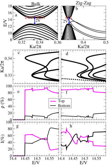
In Fig. 6 we turn our attention to the effects of the inclusion of further hoppings in the tight-binding model. These results are for a non-disordered BLG system of the same size (N=300) and same bias voltage (V=0.07 eV) considered in Fig. 2. The difference is that now we include next-nearest neighbors in each layer (eV) and also two extra interlayer coupling parameters: eV, the interlayer coupling between non-dimer sites and , and eV, the interlayer coupling between dimer and non-dimer sites and , or and McCann and Koshino (2013); Kuzmenko et al. (2009). These induce a trigonal warping and give rise to electron-hole asymmetryMcCann and Koshino (2013); A. H. Castro Neto et al. (2009), as observed inFig. 6(a) and (b). For the bulk, we see once again the opening of the energy gap of approximately 2V, due to the applied bias. The band structure is not anymore symmetrical around E/V=0, there is an energy shift of the band structure to around Nilsson et al. (2008). We can see the mixing of higher bands for this system size and bias. For the zigzag case, one can see that edge states acquire velocitySasaki et al. (2006). Fig. 6 (c) and (d) are zooms into the band structure’s regions marked by the dashed lines.
In Fig. 6(e) and (f) we show the percentage of the total charge density of the bilayer which is accumulated in each of the layers (top or bottom). Comparing them to Fig. 2(e) and (f), one observe that both for the bulk system and for the one with zigzag edges, the further hoppings here do not affect at all the polarization of charge towards the top layer. The distribution of the current density in each layer is shown in Fig. 6(g) and (h), for bulk and zigzag, respectively. One can see now that, in general, the current is not as polarized toward the bottom layer as it is for the nearest neighbor hopping seen in Fig. 2(g) and (h). Nevertheless, the unbalance between charge and current densities is still clear, and even considering the non-vertical interlayer couplings and the next-nearest intralayer hoppings, there are clear energy regions where the current flows more throughout the bottom layer. There are also switches to energy regions where the current is shared between both layers or is predominant over top layer. Further investigations are important here to elucidate the exact mechanisms causing these switches.
VII Conclusions
An external electric field perpendicular to a Bernal-stacked bilayer graphene, breaks layer and sublattice symmetry; localizing charge over two sublattices in different layers. Under this charge landscape, it is not obvious how charge current flows within the sample. We have shown here that current distribution is highly affected by the polarization of charge to only one sublattice, as well as by the geometry of the system (width considered and presence or not of edges) and by the strength of the electric field.
We demonstrate that current does not necessarily flow over regions of the system with higher charge density, even when next-nearest neighbor hoppings are included in our model. For some energy ranges, charge can be polarized to one layer, while the current is equally distributed over both layers. There are also considerable energy ranges for which the current flows predominantly over the layer with much lower charge density. We show that this effect can be explained by the sublattice polarization of charge in the AB-stacking biased BLG, and that it is robust against disorder. Therefore, to design applications of bilayer graphene in digital electronics, it is essential to calculate not only the charge distribution in each layer, but also the current density distribution in each layer, as it presents much richer details than the more monotonic behavior of the charge distribution.
Acknowledgements.
The authors are grateful to P. A. Schulz for a critical reading of the manuscript. C.J.P. acknowledges financial support from FAPESP (Brazil), A.L.C.P. acknowledges partial support from CNPq (Brazil). Part of the numerical simulations were performed at the computational facilities from CENAPAD-SP, at Campinas State University.References
- Topinka et al. (2000) M. A. Topinka, B. J. LeRoy, S. E. J. Shaw, E. J. Heller, R. M. Westervelt, K. D. Maranowski, and A. C. Gossard, Science 289, 2323 (2000), http://www.sciencemag.org/content/289/5488/2323.full.pdf .
- Topinka et al. (2001) M. A. Topinka, B. J. LeRoy, S. E. J. Westervelt, R. M.and Shaw, R. Fleischmann, E. J. Heller, and A. C. Maranowski, K. D.and Gossard, Nature 410, 183 (2001).
- A. H. Castro Neto et al. (2009) A. H. Castro Neto, F. Guinea, N. M. R. Peres, K. S. Novoselov, and A. K. Geim, Rev. Mod. Phys. 81, 109 (2009).
- Rycerz et al. (2007) A. Rycerz, J. Tworzydlo, and C. W. J. Beenakker, Nat Phys 3, 172 (2007).
- San-Jose et al. (2009) P. San-Jose, E. Prada, E. McCann, and H. Schomerus, Phys. Rev. Lett. 102, 247204 (2009).
- Akhmerov and Beenakker (2007) A. R. Akhmerov and C. W. J. Beenakker, Phys. Rev. Lett. 98, 157003 (2007).
- Gunlycke and White (2011) D. Gunlycke and C. T. White, Phys. Rev. Lett. 106, 136806 (2011).
- Schwierz (2010) F. Schwierz, Nat Nano 5, 487 (2010).
- Pesin and MacDonald (2012) D. Pesin and A. H. MacDonald, Nat Mater 11, 409 (2012).
- Castro et al. (2008) E. V. Castro, N. M. R. Peres, J. M. B. Lopes dos Santos, A. H. C. Neto, and F. Guinea, Phys. Rev. Lett. 100, 026802 (2008).
- Zârbo and Nikolić (2007) L. P. Zârbo and B. K. Nikolić, EPL (Europhysics Letters) 80, 47001 (2007).
- McCann (2006) E. McCann, Phys. Rev. B 74, 161403 (2006).
- Castro et al. (2007) E. V. Castro, K. S. Novoselov, S. V. Morozov, N. M. R. Peres, J. M. B. L. dos Santos, J. Nilsson, F. Guinea, A. K. Geim, and A. H. C. Neto, Phys. Rev. Lett. 99, 216802 (2007).
- Xu et al. (2013) D. Xu, H. Liu, V. S. IV, J. Song, H. Jiang, Q. feng Sun, and X. C. Xie, Journal of Physics: Condensed Matter 25, 105303 (2013).
- Ohta et al. (2006) T. Ohta, A. Bostwick, T. Seyller, K. Horn, and E. Rotenberg, Science 313, 951 (2006), http://www.sciencemag.org/content/313/5789/951.full.pdf .
- Nilsson et al. (2008) J. Nilsson, A. H. Castro Neto, F. Guinea, and N. M. R. Peres, Phys. Rev. B 78, 045405 (2008).
- McCann and Koshino (2013) E. McCann and M. Koshino, Reports on Progress in Physics 76, 056503 (2013).
- Zhang et al. (2009) Y. Zhang, T.-T. Tang, C. Girit, Z. Hao, M. C. Martin, A. Zettl, and Y. R. W. F. Crommie, Michael F. nad Shen, Nature 459, 820 (2009).
- Abedinpour et al. (2007) S. H. Abedinpour, M. Polini, A. H. MacDonald, B. Tanatar, M. P. Tosi, and G. Vignale, Phys. Rev. Lett. 99, 206802 (2007).
- Miyazaki et al. (2010) H. Miyazaki, K. Tsukagoshi, A. Kanda, M. Otani, and S. Okada, Nano Letters 10, 3888 (2010), http://pubs.acs.org/doi/pdf/10.1021/nl1015365 .
- Xia et al. (2010) F. Xia, D. B. Farmer, Y.-m. Lin, and P. Avouris, Nano Letters 10, 715 (2010), pMID: 20092332, http://pubs.acs.org/doi/pdf/10.1021/nl9039636 .
- J. et al. (2012) V. J., J. L., B. W., L. Y., K. P., A. V., B. M., L. C. N., V. C., S. R., S. D., F. Zhang, J. J., and M. A. H., Nat Nano 7, 156 (2012).
- Qiao et al. (2011) Z. Qiao, J. Jung, Q. Niu, and A. H. MacDonald, Nano Letters 11, 3453 (2011), http://pubs.acs.org/doi/pdf/10.1021/nl201941f .
- Li et al. (2010) X. Li, Z. Zhang, and D. Xiao, Phys. Rev. B 81, 195402 (2010).
- Kim et al. (2013) K. S. Kim, T.-H. Kim, A. L. Walter, T. Seyller, H. W. Yeom, E. Rotenberg, and A. Bostwick, Phys. Rev. Lett. 110, 036804 (2013).
- Nakada et al. (1996) K. Nakada, M. Fujita, G. Dresselhaus, and M. S. Dresselhaus, Phys. Rev. B 54, 17954 (1996).
- Lima et al. (2010) M. P. Lima, A. J. R. da Silva, and A. Fazzio, Phys. Rev. B 81, 045430 (2010).
- Lv and Li (2012) S.-H. Lv and Y.-X. Li, Journal of Applied Physics 112, 053701 (2012).
- Wang et al. (2011) M. Wang, E. B. Song, S. Lee, J. Tang, M. Lang, C. Zeng, G. Xu, Y. Zhou, and K. L. Wang, ACS Nano 5, 8769 (2011), http://pubs.acs.org/doi/pdf/10.1021/nn2027566 .
- Kuzmenko et al. (2009) A. B. Kuzmenko, I. Crassee, D. van der Marel, P. Blake, and K. S. Novoselov, Phys. Rev. B 80, 165406 (2009).
- Datta (1999) S. Datta, Electronic Transport in Mesoscopic Systems (Cambridge University Press, Cambridge, 1999).
- Ferry and Goodnick (1999) D. K. Ferry and S. M. Goodnick, Transport in Nanostructures, Cambridge Studies in Semiconductor Physics & Microelectronic Engineering, Vol. 6 (Cambridge University Press, 1999).
- Lewenkopf and Mucciolo (2013) C. H. Lewenkopf and E. R. Mucciolo, J. Comput. Electron. 12, 203 (2013).
- Bahamon et al. (2011) D. A. Bahamon, A. L. C. Pereira, and P. A. Schulz, Phys. Rev. B 83, 155436 (2011).
- Haug (2008) J. A.-P. Haug, H., Quantum Kinetics in Transport and Optics of Semiconductors (Springer Berlin Heidelberg, 2008).
- Cresti et al. (2003) A. Cresti, R. Farchioni, G. Grosso, and G. P. Parravicini, Phys. Rev. B 68, 075306 (2003).
- Metalidis and Bruno (2005) G. Metalidis and P. Bruno, Phys. Rev. B 72, 235304 (2005).
- Castro et al. (2010) E. V. Castro, K. S. Novoselov, S. V. Morozov, N. M. R. Peres, J. M. B. L. dos Santos, J. Nilsson, F. Guinea, A. K. Geim, and A. H. C. Neto, Journal of Physics: Condensed Matter 22, 175503 (2010).
- Yao et al. (2009) W. Yao, S. A. Yang, and Q. Niu, Phys. Rev. Lett. 102, 096801 (2009).
- Rhim and Moon (2008) J.-W. Rhim and K. Moon, Journal of Physics: Condensed Matter 20, 365202 (2008).
- Koshino and Ando (2006) M. Koshino and T. Ando, Phys. Rev. B 73, 245403 (2006).
- Ramasubramaniam et al. (2011) A. Ramasubramaniam, D. Naveh, and E. Towe, Nano Letters 11, 1070 (2011), http://pubs.acs.org/doi/pdf/10.1021/nl1039499 .
- Mucciolo et al. (2009) E. R. Mucciolo, A. H. Castro Neto, and C. H. Lewenkopf, Phys. Rev. B 79, 075407 (2009).
- Cresti and Roche (2009) A. Cresti and S. Roche, New Journal of Physics 11, 095004 (2009).
- Mucciolo and Lewenkopf (2010) E. R. Mucciolo and C. H. Lewenkopf, Journal of Physics: Condensed Matter 22, 273201 (2010).
- Pereira and Schulz (2008) A. L. C. Pereira and P. A. Schulz, Phys. Rev. B 77, 075416 (2008).
- Sasaki et al. (2006) K. Sasaki, S. Murakami, and R. Saito, Applied Physics Letters 88, 113110 (2006).