Novel properties of graphene in the presence of energy gap:
optics, transport and mobility studies
Abstract
We review the transmission of Dirac electrons through a potential barrier in the presence of circularly polarized light. A different type of transmission is demonstrated and explained. Perfect transmission for nearly head-on collision in infinite graphene is suppressed in gapped dressed states of electrons. We also present our results on enhanced mobility of hot Dirac electrons in nanoribbons and magnetoplasmons in graphene in the presence of the energy gap. The calculated carrier mobility for a graphene nanoribbon as a function of the bias field possesses a high threshold for entering the nonlinear transport regime. This threshold is a function of both extrinsic and intrinsic properties, such as lattice temperature, linear density, impurity scattering strength, ribbon width, and correlation length for the line-edge roughness. Analysis of non-equilibrium carrier distribution function confirms that the difference between linear and nonlinear transport is due to sweeping electrons from the right to left Fermi one through elastic scattering as well as moving electrons from low to high-energy ones through field-induced heating. The plasmons, as well as the electron-hole continuum are determined by both energy gap and the magnetic field, showing very specific features, which have been studied and discussed in details.
pacs:
73.40.Gk, 61.48.-c, 72.10.Fk, 72.20.Ht, 05.45.-a, 73.43.Lp, 78.30.NaI Introduction
A considerable amount of interest in basic research and device development has been generated for both the electronic and optical properties of two-dimensional (2D) graphene material dh-ref-1.4 ; dh-ref-2.2 ; dh-ref-2.3 ; dh-ref-2.4 ; dh-ref-2.5 . This began with the first successful isolation of single graphene layers and the related transport and Raman experiments for such layers dh-ref-2.6 . It is found that the major difference between a graphene sheet and a conventional 2D electron gas (EG) in a quantum well (QW) is the band structure, where the energy dispersions of electrons and holes in the former are linear in momentum space, but quadratic for the latter. Consequently, particles in graphene behave like massless Dirac fermions and display many unexpected phenomena in electron transport and optical response, including the anomalous quantum Hall effect dh-ref-1.2 ; dh-ref-2.8 , bare and dressed state Klein tunneling dh-ref-2.9 ; dh-ref-2.10 ; dh-ref-2.11 ; dh-ref-2.12 and plasmon excitation dh-ref-2.13 ; dh-ref-2.14 ; dh-ref-2.15 , a universal absorption constant dh-ref-2.16 ; dh-ref-2.17 , tunable intraband dh-ref-2.18 and interband dh-ref-2.19 ; dh-ref-2.20 optical transitions, broadband -polarization effect dh-ref-2.21 , photo-excited hot-carrier thermalization dh-ref-2.22 and transport dh-ref-2.23 , electrically and magnetically tunable band structure for ballistic transport dh-ref-2.24 , field-enhanced mobility in a doped graphene nanoribbon dh-ref-1.0 and electron-energy loss in gapped graphene layers dh-ref-2.26 .
Most of the unusual electronic properties of graphene may be explained by single-particle excitation of electrons. The Kubo linear-response theory dh-ref-2.27 and Hartree-Fock theory combined with the self-consistent Born approximation dh-ref-2.28 were applied to diffusion-limited electron transport in doped graphene. Additionally, the semiclassical Boltzmann theory was employed for studying transport in both linear dh-ref-1.16 and nonlinear dh-ref-1.0 regimes. For the plasmon excitation in graphene, its important role in the dynamical screening of the electron-electron interaction dh-ref-2.13 ; dh-ref-2.14 ; dh-ref-2.15 ; dh-ref-2.26 ; dh-ref-2.30 has been reported. However, relatively less attention has been received for the electromagnetic (EM) response of graphene materials, especially for low-energy intraband optical transions dh-ref-2.18 ; dh-ref-2.31 ; dh-ref-2.32 .
Gapped graphene has marked an important milestone in the study of graphene’s electronic and transport properties from both a theoretical and experimental point of view as well as in practical device applications. The reason for this is that gapped graphene has applications such as a field-effect transistor where a gap is essential as well as graphene interconnects. The effective band gap may be generated by spin-orbit interaction, or when monolayer graphene is placed on a substrate such as ceramic silicon carbide or graphite. The gap may also arise dynamically when graphene is irradiated with circularly polarized light. Depending on the nature of the substrate on which graphene is placed or the intensity or amplitude of the light, the gap may be a few meV or as large as one eV bib:AI:Kibis . In general, the energy gap is attributed to a breakdown in symmetry between the sublattices caused by external perturbing fields from the substrate or photons coupled to the atoms in the and sublattices.
This Section will be divided into two parts covering the electrical and optical properties of electrons in gapped graphene materials. The first part will deal with electrical transport. Topics will include: (1) unimpeded tunneling of chiral electrons in graphene nanoribbons; (2) anomalous photon-assisted tunneling of Dirac electrons in graphene; and (3) field enhanced mobility by nonlinear phonon scattering of Dirac electrons. The second part will focus on the collective plasmon (charge density) excitations for: intraband and interband plasmons.
II Dirac Fermions in Graphene: Chirality and Tunable Gap
Graphene, an allotrope of carbon, which has been recently discovered in experiment dh-ref-1.2 , has become one of the most important and extensively studied materials in modern condensed matter physics, mainly because of its extraordinary electronic and transport properties bib:AI:Katsnelson . According to Ref. bib:AI:geim:2009 , graphene can be described as a single atomic plane of graphite, which is sufficiently isolated from its environment and considered to be free-standing. The typical carbon-carbon distance in a graphene layer is nm, and the interlayer distance in a graphene stack is nm. Any graphene sample with less than carbon atoms or less than nm of length is unstable bib:AI:structure , tending to convert to other fullerenes or carbon structures. Now, we will briefly discuss the most crucial electronic properties of graphene, relevant to the electron tunneling phenomena. A good description of the principal electronic structure and properties may be found in Refs. dh-ref-1.4 ; bib:AI:DSTranspG . Surprisingly, the first theoretical study of “graphene” was performed more than sixty years ago bib:AI:Wallace1947 ; bib:AI:mcclure . The most striking difference in comparison with conventional semiconductors or metals is the fact that low-energy electronic excitations in graphene are massless with Dirac cones for energies. The quite complicated energy band structure of graphene may be approximated as a cone (Dirac cone) in the vicinity of the two inequivalent corners, i.e., and points, of the Brillouin zone. In summary, the electronic properties of graphene may be approximately described by the Dirac equation, corresponding to the linear energy dispersion next to the and points:
| (1) |
where is the Fermi velocity. This form is similar to the high-energy quantum electrodynamics (QED) Dirac equation. In momentum () space, the Hamiltonian is simplified as follows:
| (2) |
Here, is a uniform external potential. We will also adapt the following notation: . The energy dispersions are simply and gapless. In addition, is the electron-hole parity index 222The quantity is often called pseudo-spin because of its formal resemblance to the spin index in a spinor wavefunction., so that for electrons and for holes.
The goal of this Section is to compare the electronic and transport properties of gapped graphene modeled by finite electron effective mass with those obtained in the case of massless Dirac fermions. There have been many studies bib:AI:substrate ; bib:AI:gapstun , where the mass term is added to the Dirac Hamiltonian of infinite graphene. An energy gap may appear as a result of a number of physical reasons, such as by a boron nitride substrate. However, the most interesting cases are when the gap becomes tunable and may be varied throughout the experiment, resulting in practical applications. We will focus on the so-called electron-photon dressed states, which result from the interaction between Dirac electrons in graphene and circularly-polarized photons. The first complete quantum description of such a system was presented in Ref. bib:AI:Kibis , and the transport properties were discussed in Ref. bib:AI:kibis2 . The quantum descriptions for both graphene dh-ref-2.11 and three-dimensional topological insulators were further developed in Ref. bib:AI:mine2 .
III Tunneling in Gapped Graphene
The so-called Klein paradox is related to complete unimpeded transmission of Dirac fermions through square potential barriers of arbitrary height and width in the case of head-on collision. It has been demonstrated that certain aspects of the Klein paradox may also be observed in bilayer graphene bib:AI:Katsnelson , carbon nanotubes, topological insulators bib:AI:mine2 and zigzag nanoribbons dh-ref-2.11 . The trademark of the Klein paradox exists even in the case of electron-photon dressed states for massive electrons dh-ref-2.11 .
III.1 Klein Paradox for the Square Barrier Tunneling
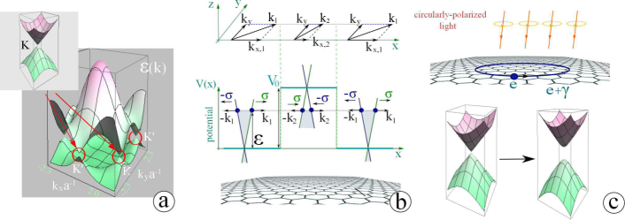
In order to demonstrate Klein tunneling and investigate its unique properties, we will consider a sharp potential barrier (like a junction), given by and infinite in the direction specified by the Heaviside step function . Here, we will use the notations introduced in Fig. 1(b).
Klein tunneling may be explained based on a specific form of the Dirac fermion wavefunction as well as a special type of chiral symmetry of the Dirac Hamiltonian. The eigenvalue wavefunctions obtained from Eq. (1) are and
| (3) |
Electrons are said to be chiral if their wavefunctions are eigenstates of the chirality operator , where is the Pauli vector consisting of the Pauli matrices and is the electron momentum operator in graphene layers. Electrons become chiral in graphene due to the fact that the chirality operator is proportional to the Dirac Hamiltonian which automatically makes chirality a good quantum number. One can easily verify that the wavefunction in Eq. (3) satisfies the chirality property.
As an example, we consider the situation of a very high potential barrier, i.e., , which would not allow any finite transmission amplitude possible for a conventional Schrödinger particle. For Dirac electrons, however, we have
| (4) |
where is the angle which makes with the -axis. Incidentally, for the case of head-on collision with , we find complete unimpeded tunneling with , which is a direct consequence of a special form of the electron wavefunction, resulting from the Dirac cone energy dispersion.
IV Electron-Photon Dressed States with Gap
The peaks of transmission mainly belong to two different species. Namely, the Klein paradox for head-on collision where and the so-called “transmission resonances” correspond to specific values of the electron longitudinal momenta in the barrier region.
It was shown recently bib:AI:Kibis ; bib:AI:kibis2 that when Dirac electrons in a single graphene layer interact with an intense circularly polarized light beam, electron states will be dressed by photons. Here, we investigate the transmission properties of such dressed electrons for the case of single layer graphene.
We begin with the electron-photon interaction Hamiltonian
| (5) |
where the vector potential for circularly polarized light of frequency may be expressed as
| (6) |
in terms of photon creation and destruction operators and , respectively. Here, is the mode volume of an optical field. In order to study the complete electron-photon interacting system, we must add the field energy term to the Hamiltonian Eq. (5).
In terms of the energy dispersion , our system is formally similar to the eigenvalue equations for the case of the effective mass Dirac Hamiltonian:
| (7) |
where is a Pauli matrix and is a one-dimensional potential. The electron dispersion and transmission properties for both a single and multiple square potential barrier have been studied bib:AI:Barb-review ; bib:AI:Barb2 for monolayer and bilayer graphene. It was also shown that a one-dimensional periodic array of potential barriers leads to multiple Dirac points bib:AI:Barb-review . Several published works have introduced an effective mass term into the Dirac Hamiltonian for infinite graphene, which may be justified based on different physical reasons bib:AI:gapstun ; bib:AI:pnp . For example, it has been shown bib:AI:substrate that an energy band gap in graphene can be created by boron nitride substrate, resulting in a finite electron effective mass. However, we would like to emphasize that the analogy between the Hamiltonian Eq. (7) and that for irradiated graphene is not complete since the former requires . Although this difference does not result in any modification of the energy dispersion term containing , it certainly changes the corresponding wavefunction. Additionally, there have been a number of studies using laser radiation on single layer bib:AI:r1 and bilayer bib:AI:Luis1 graphene as well as graphene nanoribbons bib:AI:c1 reporting the gap opening as a result of strong electron-photon interaction. From these aspects, it seems that topological insulators as well as gapped graphene may have potential device applications where spin plays a role. In the presence of a strong radiation field, we have the dressed-state wavefunction
| (8) |
where and are given by
| (9) | |||
| (10) |
Here, . Consequently, the chiral symmetry is broken for electron dressed states. The interaction between Dirac electrons in graphene and circularly polarized light has been considered in the classical limit in Ref. bib:AI:aoki_oki . In this limit, a gap in the Dirac cone opens up due to nonlinear effects. The dressed-state wavefunction has the chirality
| (11) |
As it appears, non-chirality of the dressed electron states becomes significant if the electron-photon interaction (the leading term) is increased. This affects electron tunneling and transport properties. We now turn to an investigation of the transmission of electron states through a potential barrier when graphene is irradiated with circularly polarized light.
Summarizing the description of the electron dressed states, we would like to estimate the actual values of the energy gap in graphene and describe its dependence on the power and the frequency of the applied laser beam, which obeys the equation:
| (12) |
where , so that the gap is proportional to the square of amplitude of the electric field for . The amplitude of the electromagnetic field is determined by the laser power and its wavelength . Consequently, the energy gap in graphene depends on both the power of the applied laser and its wavelength. The results could be summarized in the following table:
| m | m | m | |
|---|---|---|---|
| P = 0.1 W | 0.027 | 0.274 | 2.71 |
| P = 1 W | 0.264 | 2.738 | 25.03 |
| P= 100 W | 27.39 | 249.14 | 709.213 |
IV.1 Tunneling and Optical Properties of Electron Dressed States
We consider a square potential barrier given by . The current component is , thus we only require the wave-function continuity at the potential boundaries. There are two specific simplifications to consider here - a nearly-head-on collision and the case of a high potential barrier when . We should also mention another relevant study bib:AI:gomes , investigating the tunneling of Dirac electrons with a finite effective mass through a similar potential barrier.
For a nearly-head-on collision with for high potential as well as infinite graphene (), the transmission coefficient has the following simplified form
| (13) |
where we assume , and .
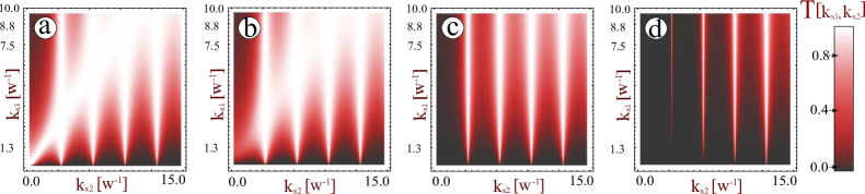
Figure 2 presents the calculated transmission probability as a function of the longitudinal momenta (in front the barrier) and (in the barrier region). We find from Fig. 2 that the intensity of the transmission peaks in (b)-(d) are gradually distorted with increasing gap compared to infinite graphene in (a). The diagonal corresponds to the absence of a potential barrier and should yield a complete transmission for as seen in (a). However, for a finite , the requirement must be satisfied, which makes the diagonal transmission incomplete, e.g., missing diagonal for small and in (b), due to the occurrence of an energy gap. As is further increased in (c) and (d), this diagonal distortion becomes more and more severe, which is accompanied by strongly reduced intensity of transmission peaks at small .
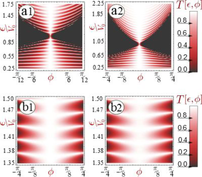
Figure 3 displays the effect of the energy gap on in terms of incoming particle energy and angle of incidence . From the upper panel of Fig. 3(a1)-(a4), we see the Klein paradox as well as other resonant tunneling peaks in for regular infinite graphene with . The dark “pockets” on both sides of demonstrate zero transmission for the case of , which results in imaginary longitudinal momentum for most of the incident angles and produces a fully attenuated wavefunction.
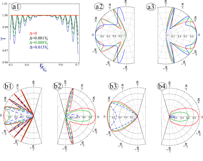
Figure 4 shows as a function of in (a1) and of in all other plots. From (a1), we clearly see that dressing destroys the Klein paradox for head-on collision with . Additionally, in the absence of electron-photon interaction, we display the effects on for various values of in (a2) and in (a3). The resonant peaks are found to be shifted toward other incoming angles in both (a2) and (a3) and this effect becomes stronger for small incident angles. The effect of dressed electron states, on the other hand, is demonstrated in each plot in (b1)-(b4) for various values of , as well as in individual plots of (b1)-(b4) for different barrier heights and widths .
It is very helpful to compare the results obtained here with bilayer graphene having quadratic dispersion. For bilayer graphene, its lowest energy states are described by the Hamiltonian bib:AI:Katsnelson
| (14) |
where is the effective mass of electrons in the barrier region. In this case, the longitudinal wave vector component in the barrier region is given by with , .
An evanescent wave having a decay rate may coexist with a propagating wave having a wave vector such that . This implies that the evanescent modes should be taken into account simultaneously. The Klein paradox persists in bilayer graphene for chiral but massive particles. However, one finds a complete reflection, instead of a complete transmission, in this case.
In the simplest approximation to include only the two nearest subbands, our model is formally similar to the so-called Hamiltonian used for describing the particles in a single layer of graphene with parabolic energy dispersion (non-zero effective mass). By including more than two independent pairs, this effect is expected to be weaker since perfect transmission will occur only for the two wavefunction terms. However, this effect is insensitive to the barrier width, and therefore, may be considered as reminiscent of the Klein paradox.
In spite of the fact that a significant number of papers on electron tunneling in the presence of the electron-photon interaction have already been published, this topic is receiving a lot of attention at the present time. Potential barrier transmission is studied using the Floquet approach bib:AI:Bis ; bib:AI:Hungary . It is appears that the valley of the massive Dirac electrons could become an important factor for the square barrier tunneling. Valleytronics uses the valley degree of freedom as a carrier of information similarly to the way spintronics uses electron spin Moldovan
The effect of periodic potential is similar to the combination of the uniform magnetic and electric fields bib:AI:HofsConf . Also we would like to mention Ref.bib:AI:Mod , where the transport properties were investigated in the framework of unitary-transformation scheme together with the non-equilibrium Green’s function formalism. Similar case of Chiral tunneling modulated by a time-periodic potential on the surface states of a topological insulator was addressed in bib:AI:Nature2 .
In conclusion, we would like to mention topological insulators. Due to their band structure and a nontrivial topological order, topological insulators are insulating in the bulk, but support gapless conducting surface states bib:AI:HasanTI . The surface states are represented by a spin-polarized Dirac cone, creating an analogy with graphene. However, there is a peculiar property of the topological insulator, i.e., a so-called geometrical gap in the energy dispersion. This gap appears if the sample is finite in the -direction, which has not been observed in conventional insulators. The electron dressed states in three dimensional topological insulators have been obtained and their tunneling properties have been discussed bib:AI:mine2 ; bib:AI:mySPIE .
V Enhanced Mobility of Hot Dirac Electrons in Nanoribbons
Early studies dh-ref-1.16 ; dh-ref-1.11 on transport in graphene nanoribbons (GNRs) were restricted to the low-field limit dh-ref-1.01 , where a linearized Boltzmann equation with a relaxation-time approximation was solved. Recently, the non-equilibrium distribution of electrons is calculated by solving the Boltzmann equation beyond the relaxation-time approximation for nonlinear transport in semiconducting GNRs dh-ref-1.02 . Enhanced mobility from field-heated electrons in high energy states is predicted. An anomalous enhancement in the line-edge roughness scattering under high fields is found with decreasing roughness correlation length due to the population of high-energy states by field-heated electrons dh-ref-1.0 .
V.1 Nonlinear Boltzmann Theory
We limit ourselves to single subband transport with low electron densities, moderate temperatures, ionized impurities and line-edge roughness dh-ref-1.16 ; dh-ref-1.18 ; dh-ref-1.19 . Consequently, negligible influences from electron-electron dh-ref-1.20 , optical phonon dh-ref-1.19 , inter-valley and volume-distributed impurity scattering dh-ref-1.16 are expected. The discrete energy dispersion for Armchair-nanoribbons (ANRs) is written as dh-ref-1.4
| (15) |
The discrete wave numbers are with for a large odd integer , and is mesh spacing. The central point is for the minimum of the energy. is the GNR width, Å the size of the graphene unit cell, and the number of carbon atoms across GNRs. From Eq. (15), we get for the group velocity for metallic nanoribbons, while for semiconducting ANRs, it is . We know the band will be filled up to at zero temperature ( K) with the Fermi wave number and Fermi energy given, respectively, by and . For a chosen and chemical potential , the linear density in ANRs is .
We assume that the wavefunction corresponding to Eq. (15) satisfies hard-wall boundary conditions dh-ref-1.21 . This can be fulfilled by selecting the wavefunction as a mixture of ones at and points as dh-ref-1.4
| (16) |
| (17) |
Here, is the ribbon length. For semiconducting ANRs is the quantum of the transverse wave vector, and the phase separation between the two graphene sublattices. For a metallic-type ribbon, we set and the phase assumes only values.
With the wavefunction in Eq. (16) and neglecting inter-valley scattering 333Such inter-valley scattering would require momentum transfer comparable with the distance between and points. one may calculate the scattering from any potential . The impurity and phonon induced inter-valley scattering is neglected because the relevant phonon energy for momentum transfer is large at low temperatures and the effective scattering cross section of both volume and surface impurities is suppressed for large value of . Therefore, the interaction matrix elements become
| (18) |
We consider scattering potential made from the three contributions to be .
Since the longitudinal phonons induce higher deformation potential than the out-of-plane flexural ones, we neglect the flexural modes here. Under this approximation, the phonon-scattering potential is written as dh-ref-1.16 ; dh-ref-1.23
| (19) |
where and are the equilibrium phonon distributions, the phonon frequency, eV the deformation potential, g/cm2, and cm/s the mass density and sound velocity. Moreover, the momentum conservation gives .
Elastic scattering is attributed to the roughness of the ribbon edges and in-plane charged impurities. For the former, we assume the width of the ribbon as and the edge-roughness to satisfy the Gaussian correlation function with Å being the amplitude and Å the correlation length. The latter is related to impurities located at and distributed with a sheet density . Each point impurity produces a scattering potential. Since the momentum difference between two valleys is very large, only short-range impurities can contribute. Here, we neglect the short range scatterers thus making the scattering matrix diagonal. Corresponding perturbations for roughness and impurity are
| (20) | |||||
| (21) | |||||
| (22) |
where is the average host dielectric constant.
These potentials provide the net elastic scattering rate through
{gather}
1τj = 1τimpj+1τLERj ,
\notag
{
(τ^imp_j)^-1=γ_0 (vF—vj—)[1+cos(2ϕ_j)](τ^LER_j)^-1=γ_1 (vF—vj—)11+4kj2Λ02[1+cos(2ϕ_j)] ,
where is the scattering rate of impurities at the Fermi edge
and the scattering rate from edge
roughness. Here, we assume the impurities distribute within the layer.
Moreover, the scattering potential is screened by electrons. Since we limit ourselves to a single subband, the screening is just
a scalar Thomas-Fermi dielectric function dh-ref-1.16 ; dh-ref-1.26
, which is
calculated as
in the metallic limit () with .
We apply the static screening to both impurity and phonon scattering
with a relative large damping rate and small Fermi energy.
The deviation from the Fermi distribution under a strong field is described by the nonlinear Boltzmann equations dh-ref-1.18 ; dh-ref-1.19
| (23) |
where is the reduced form of the non-equilibrium part 444A distinct line must be drawn between equilibrium distribution function in absence of applied electric field and stationary solution of the transport equation . of the distribution. This reduced form ensures conservation of particle numbers, i.e. . Equation (23) was used for investigating the dynamics in quantum wires dh-ref-1.18 and quantum-dot superlattices dh-ref-1.19 . In Eq. (23), we introduced notation for the matrix elements via its components
| (24) | |||||
| (25) |
The total inelastic rate is with the scattering matrix
| (26) |
| (27) |
Here, we employ the notations , , , and is the Bose function for phonons. Moreover, the nonlinear phonon scattering rate , associated with the heating of electrons, is
| (28) |
Once is obtained from Eq. (23), the drift velocity is found from
| (29) |
One knows that the equilibrium part of the distribution does not contribute to the drift velocity. The steady-state drift velocity is obtained from in the limit . Furthermore, the steady-state current is given by . The differential mobility is defined as .
V.2 Numerical Results for Enhanced Hot-Electron Mobility
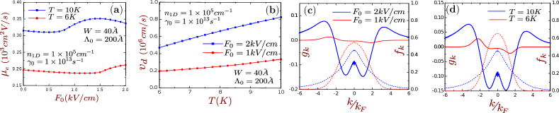
Figure 5(a) displays the mobilities as a function of at K and K. We see from Fig. 5(a) a strong -dependence at a lower value of and at higher temperature . The observed feature comes from the electron-phonon scattering rate in Eq. (28). We find a lower threshold field is needed for entering into a nonlinear regime () because of enhanced phonon scattering at K. strongly depends on , , and . As , is larger at K than at K since there exists an additional thermal population of high-energy states with a high group velocity. The initial reduction of is connected to the increased frictional force with from phonon scattering. We can see is independent of below kV/cm (linear regime) at K. However, goes up significantly above kV/cm (nonlinear regime). Finally, drops with beyond kV/cm (heating regime), giving rise to a saturation of the drift velocity. From Eq. (15) we understand the group velocity increases with . However, this increase becomes slower as approaching to . Physically, the rise of with in the nonlinear regime comes from the initially-heated electrons in high energy states with a larger group velocity, while the successive drop of in the heating regime connects to the combination of the upper limit and the significantly enhanced phonon scattering. In Fig. 5(b), is presented as a function of at kV/cm and kV/cm. increases with monotonically in both cases, proving that the scattering is not dominated by phonons but by impurities and line-edge roughness. Different features in the increase of are attributed to the linear and nonlinear regimes. For kV/cm in the nonlinear regime, (or ) increases with sub-linearly, while goes up super-linearly with in the linear regime at kV/cm. Different dependence in directly connects to , displayed in Figs. 5(c) and 5(d). at K, as well as the total distribution function , are exhibited in Fig. 5(c) as functions of at kV/cm and kV/cm. The electron heating is found from Fig. 5(c) at kV/cm by moving thermally driven electrons from low to high-energy states with heat resulting from the work done by a frictional force dh-ref-1.23 due to phonon scattering. At kV/cm, we find electrons swept by elastic scattering from the right Fermi edge to the left one in the linear regime. Figure 5(d) demonstrates a comparison between and at K and K under kV/cm, showing that phonon scattering is important at K, while the elastic scattering of electrons dominates at K, which agrees with the observation in Fig. 5(c).
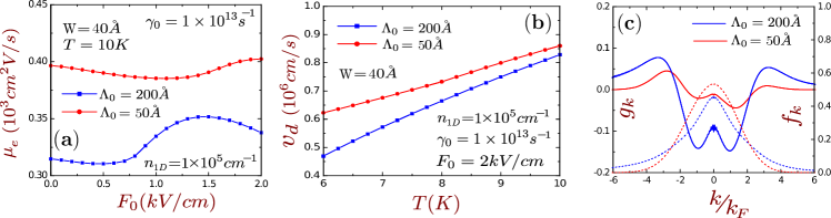
The correlation-length effect for the line-edge roughness (LER) is shown in Figs. 6(a)-(c) by setting Å and varying from Å through Å. We know from Eq. (V.1) that the LER scattering may either decrease or increase with , depending on or . For cm-1, we know is met in the low-field limit (), while we have for the high field limit due to electron heating. Consequently, we see from Fig. 6(a) increases as when is Å in the low-field regime. However, increases in the high-field regime for Å. This is accompanied by a reduction in the enhancement of . The anomalous feature with gives a profound impact on the -dependence of as shown in Fig. 6(b), where the rising rate of with in the high-field regime is much smaller with Å than for Å. Additionally, in Fig. 6(c) exhibits an anomalous cooling behavior, i.e. with a smaller spreading of in the space, in the high-field regime as drops to Å.
VI Magnetoplasmons in Gapped Graphene
Electronic and transport proprieties of Dirac electrons in the presence of a uniform perpendicular magnetic field have been reported in a few studies bib:AI:MFReviewGoerbig ; bib:AI:MFReviewKrotov ; bib:AI:Gus1 . The wavefunction, obtained in bib:AI:MFAndo1 , has a number of novel and intriguing properties. Additionally, electron-electron Coulomb interaction is found to have effects on both the quasiparticle effective mass and collective excitations bib:AI:GGGfactor . Using the same method as for the case of circularly-polarized light radiation in Eq. (1), we further take into account the vector potential for a uniform perpendicular magnetic field, giving
| (30) | |||||
In the case of 2DEG, on the other hand, the Hamiltonian contains the effective electron mass :
| (31) |
with similar canonical momentum substitution.
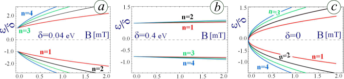
Although the energy levels are equidistant for 2DEG with (), and the cyclotron frequency, in graphene the difference between two consecutive energy levels decreases with the index of the level as , i.e., . Here . Also, will be used as a unit of frequency for both the 2DEG and graphene. These eigenenergies apparently depend on the applied magnetic field and are presented in Fig. 7. The dependence becomes the strongest for the case of zero gap in (c) and negligible with a large gap in (b).
In order to obtain the one-loop polarization function , we perform a summation over all possible transitions between the states on both sides of the Fermi energy, so that both occupied and unoccupied states will be included. The coefficients in the summations, representing the weight of each term, are called the oscillator strengths or form factors. Obviously for two well-separated eigenstates with , their coefficients become infinitesimal, which in leading order may be expressed as a factorial function . The general definition of the form factor is the wavefunction overlap, i.e.,
| (32) |
where . We will directly write down the expressions for form factors of both 2DEG and graphene. In the case of 2DEG, the form factor is calculated as
| (33) | |||||
where is the lesser of two integers and while is the greater. In the case of gapped graphene with , the form factor becomes
| (34) |
For the case of zero energy gap, , one may easily obtain the standard expression for the form factor in graphene, similar to the results in Ref. bib:AI:Rafael0 ; bib:AI:Rafael1 ; bib:AI:Pyat2 . The function contains two principal parts, i.e., the , vacuum polarization corresponding to interband transitions in undoped graphene, as well as another part involving the summation over all the occupied Landau level ( is the highest occupied Landau level)), taking into consideration the intraband transitions.
Our goal is to explore both incoherent (particle-hole modes) and coherent (plasmons) excitations in the system. The imaginary part of defines the structure factor , i.e.,
| (35) |
The particle-hole mode region is obtained from the condition . Additionally, the plasmons become damping free only if they stays away from the particle-hole mode region, or equivalently, . On the other hand, the plasmon frequencies are defined by the zeros of the dielectric function . Here, is the Fourier-transformed unscreened Coulomb potential and is the background dielectric constant. These plasmons may also be obtained from the peak of the renormalized polarization for interacting electrons in the random-phase approximation (RPA), giving
| (36) |
We note that a metal-insulator transition may also occur under a magnetic field bib:AI:MFGapGorbar , similar to the effect of circularly-polarized light, along with other effects bib:AI:MFFertig1 ; bib:AI:MFFertig2 ; bib:AI:MFAndo2 .
VI.1 Single-Particle Excitations and Magnetoplasmons
We now present and discuss our numerical results of both and for various values of chemical potentials (or equivalently, number of occupied Landau levels ) and energy gap . The disorder broadening is set to be for all our numerical calculations. One of the major effects found in our numerical results is the magnetoplasmon for various energy gaps, compared with those for gapless graphene (Dirac cone). We also compare for interacting electrons with non-interacting with various interaction parameters for 2DEG and for graphene as well.
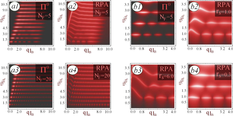
It is interesting to compare the results in the presence of an external magnetic field with those at zero magnetic field dh-ref-2.13 ; dh-ref-2.14 ; bib:AI:mySPIE ; GG:PLAS:SOI-2 for both 2DEG and gapped graphene. We emphasize that the boundaries of the particle-hole continuum are drastically different for the 2DEG and graphene. Whereas the edges of the particle-hole excitation region of 2DEG are parabolic, as seen from Fig. 8), these boundaries change to either straight lines in graphene (zero gap) or to be slightly modified by the gap. Consequently, the plasmon region defined by in graphene is significantly increased even for a small energy gap , in comparison with that for 2DEG. This demonstrates a large influence by a finite magnetic field on both the particle-hole excitation spectrum and the boundaries of the particle-hole mode regions at the same time.
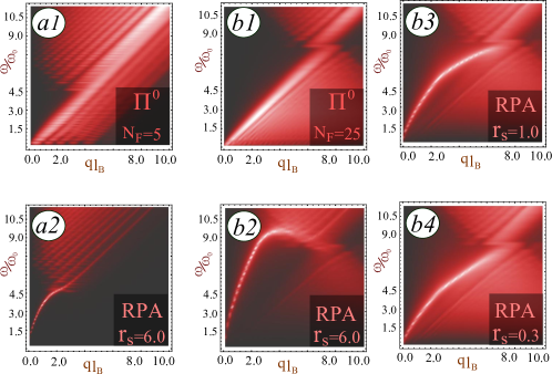
Comparing Fig. 8 with Fig. 9, we conclude that there exist two competing types of particle-hole excitation spectral behavior. These are the horizontal lines with embedded islands for 2DEG and the inclined lines for graphene. All the lines are well aligned with the boundaries of particle-hole mode regions at zero-field, including parabolic curves for 2DEG, straight lines for gapless graphene or nearly-straight lines for gapped graphene. We note that the modulation for horizontal lines in 2DEG becomes strongest, in comparison with the inclined line in graphene. This difference is attributed to the fact that the Landau levels in graphene are not equidistant in contrast to those in 2DEG. Additionally, horizontal modulation prevails for a small broadening parameter , which has been verified experimentally for the range of within –.
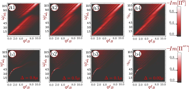
The particle-hole modes for gapless graphene with Dirac cone dispersion relation are presented in Fig. 9. The excitation regions are basically determined by the inclined straight lines obeying . A dark triangular region, located near the origin, indicates the undamped plasmons. Although non-dispersive particle-hole modes are not clearly seen, they still alter the particle-hole excitation spectrum at . The damping-free plasmon curve occurring in follows the -dispersion in the long-wavelength limit, switching to a straight line to become damped plasmons. Similar features are found from Figs. 9(b1) and (b2) for higher doping. However, the increased enlarges the region for undamped plasmons. Moreover, the RPA renormalization displayed in Figs. 9((b2)-(b4) is most significant for a larger value of interaction parameter . From Figs. 9 and 8, we also compare the RPA effects () with various values of the interaction parameter for graphene and 2DEG. The Coulomb interaction in 2DEG leads to the existence of dispersive magnetoexcitons. In the limit of vanishing interaction , however, the renormalized RPA polarization becomes similar to that of non-interacting electrons, as seen from the comparisons of (b1) and (b4) in Fig. 8 as well as in Fig. 9. Finally, Fig. 10 shows the effect on the plasmons in graphene, where the undamped plasmon curve does not follow the line anymore but follows that for instead, leading to a suppression of magnetic field effects. Collective excitations in AA- and AB-stacked graphene in the presence of magnetic field have been investigated recently by Wu.et.al bib:AI:Stack . The groupings of the Landau levels lead to considerable differences in the plasmon excitation energies, which are determined by the way in which the layers are stacked. In general, plasmonics in carbon-based nanostructures has recently received considerable development. First, plasmons modes were caclulated and studied in AA-stacked bilayer graphene bib:AI:RafaelBi . The above mentioned Klein tunneling in this type of bilayer graphene was adressed in bib:AI:AA Plasmon excitations of a single molecule, induced by an external, fast moving electron, were theoretically studied based on quantum hydrodynamical model bib:AI:Zoran1 . This study resulted in finding the differential cross sections. The localization of charged particles by the image potential of spherical shells, such as fullerene buckyballs, has been addressed in bib:AI:ourI Systems without spherical symmetry demonstrate anisotropy and dimerization of the plasmon excitations bib:AI:ourp1 ; bib:AI:ourp2 . Plasmon frequencies of such systems depend not only on the angular momentum , but its projection on the axis of quantization. Collective excitations in the processes of photoionization and electron inelastic scattering were addressed in bib:AI:V .
VII Concluding Remarks and Research Outlook
In summary, we reviewed the effect of an energy gap on the electronic, transport and many-body properties of graphene. The gap may be generated by a number of means in graphene and topological insulators. This includes a substrate or finite width. However, we paid attention to the gap which appears as a result of electron-photon interaction between Dirac electrons in graphene and circularly-polarized photons. This type of energy gap is tunable and may be varied in experiment with the intensity of the imposed light.
We note that the presence of the gap in the energy dispersion leads to the breaking of chiral symmetry. Consequently, this leads to significant changes in the electron transmission. There is a decrease of the electron transmission amplitude for a head-on collision and almost head-on incidence as a result of the fact that the Klein paradox no longer exists. The transmission resonances (the peaks for finite angles of incidence) are slightly shifted although the general structure of the peaks remains unaffected. However, if two or more pairs of subbands are taken into consideration, the transmission may even i ncrease compared to the case of only one photon.
We showed a minimum mobility before a field threshold for entering into the nonlinear-transport regime due to build-up of a frictional force. We demonstrated a mobility enhancement after this threshold value because of heated electrons in high energy states. We also obtained a maximum mobility enhancement due to balance between simultaneously increasing group velocity and phonon scattering. Additionally, we proved a increased field threshold by a small correlation length for the line-edge roughness.
Also, we considered magnetoplasmons in gapped graphene and concluded that similar to the case of zero magnetic field, the presence of the gap increases the region free from particle-hole excitations. Consequently, the region where undamped plasmons exist is expanded. We obtained a new type of plasmon dispersion.
Acknowledgements This research was supported by a grant from the AFOSR and a contract from the AFRL. We are grateful to Mary Michelle Easter for a critical reading of the manuscript and helpful comments.
References
- (1) A. H. C. Neto, F. Guinea, N. M. R. Peres, K. S. Nonoselov and A. K. Geim, Rev. Mod. Phys. 81, 109-162 (2009).
- (2) Special issue on “Electronic and photonic properties of graphene layers and carbon nanoribbons”, (Edited by G. Gumbs, D. H. Huang and O. Roslyak), Phil. Trans. R. Soc. A 138, No. 1932 (2010).
- (3) D. S. L. Abergel, V. Apalkov, J. Berashevich, K. Ziegler and T. Chakraborty, Adv. Phys. 59, 261-482 (2010).
- (4) M. Orlita and M. Potemski, Semicond. Sci. Technol. 25, 063001(22) (2010).
- (5) S. Das Sarma, S. Adam, E. H. Hwang and E. Rossi, Rev. Mod. Phys. 83, 407-470 (2011).
- (6) K. S. Novoselov, A. K. Geim, S. V. Morozov, D. Jiang, M. I. Katsnelson, I. V. Grigorieva, S. V. Dubonos and A. A. Firsov, Sci. 306, 666-669 (2004).
- (7) K. S. Novosolev, A. K. Geim, S. V. Morozov, D. Jiang, M. I. Katsnelson, I. V. Grigorieva, S. V. Dubonos and A. A. Firsov, Nat. (London) 438, 197-200 (2005).
- (8) Y. Zhang, Y.-W. Tan, H. L. Störmer and P. Kim, Nat. (London) 438, 201-204 (2005).
- (9) M. I. Katsnelson, K. S. Novoselov and A. K. Geim, Nat. Phys. 2, 620-625 (2006).
- (10) A. F. Young and P. Kim, Nat. Phys. 5, 222-226 (2009).
- (11) Roslyak, O., Iurov, A., Gumbs, G. and Huang, D., Journal of Physics: Condensed Matter, 22(16), 165301 (2010).
- (12) A. Iurov, G. Gumbs, O. Roslyak and D. H. Huang, J. Phys.: Condens. Matt. 24, 015303(8) (2012).
- (13) B. Wunsch, T. Stauber, F. Sols and F. Guinea, New J. Phys. 8, 318(15) (2006).
- (14) E. H. wang and S. Das Sarma, Phys. Rev. B 75, 205418(6) (2007).
- (15) O. Roslyak, G. Gumbs and D. H. Huang, J. Appl. Phys. 109, 113721(8) (2011).
- (16) K. F. Mak, M. Y. Sfeir, Y. Wu, C. H. Lui, J. A. Misewich and T. F. Heinz, Phys. Rev. Lett. 101, 196405(4) (2008).
- (17) R. R. Nair, P. Blake, A. N. Grigorenko, K. S. Novoselov, T. J. Booth, T. Stauber, N. M. R. Peres and A. K. Geim, Sci. 320, 1308 (2008).
- (18) L. Ju, B. Geng, J. Horng, C. Girit, M. Martin, Z. Hao, H. A. Bechtel, X. Liang, A. Zettl, Y. R. Shen and F. Wang, Nat. Nanotechn. 6, 630-634 (2011).
- (19) Z. Q. Li, E. A. Henriksen, Z. Jiang, Z. Hao, M. C. Martin, P. Kim, H. L. Störmer and D. N. Basov, Nat. Phys. 4, 532-535 (2008).
- (20) F. Wang, Y. Zhang, C. Tian, C. Girit, A. Zettl, M. Crommie and Y. R. Shen, Sci. 320, 206-209 (2008).
- (21) Q. Bao, H. Zhang, B. Wang, Z. Ni, C. Haley, Y. X. Lim, Y. Wang, D. Y. Tang and K. P. Loh, Nat. Photonics, 5, 411-415 (2011).
- (22) J. H. Strait, H. Wang, S. Shivaraman, V. Shields, M. Spencer and F. Rana, Nano Lett. 11, 4688-4692 (2011).
- (23) J. C. W. Song, M. S. Rudner, C. M. Marcus and L. S. Levitov, Nano Lett. 11, 4902-4906 (2011).
- (24) O. Roslyak, G. Gumbs and D. H. Huang, Phys. Lett. A 374, 4061-4064 (2010).
- (25) D. H. Huang, G. Gumbs and O. Roslyak, Phys. Rev. B 83, 115405(9) (2011)
- (26) O. Roslyak, G. Gumbs and D. H. Huang, Physica E 44. 1874-1884 (2012).
- (27) J. Z. Bernád, M. Jääskeläinen and U. Zülicke, Phys. Rev. B 81, 073403(4) (2010).
- (28) K. Nomura and A. H. MacDonald, “Quantum Hall Ferromagnetism in Graphene”, Phys. Rev. Lett. 96, 256602(4) (2006).
- (29) T. Fang, A. Konar, H. Xing and D. Jena, Phys. Rev. B 78, 205403(8) (2008).
- (30) A. Bostwick, F. Speck, T. Seyller, K. Horn, M. Polini, R. Asgari, A. H. MacDonald and E. Rotenberg, Sci. 328, 994-999 (2010).
- (31) S. A. Mikhailov and K. Ziegler, Phys. Rev. Lett. 99, 016803(4) (2007).
- (32) M. Jablan, H. Buljan and M. Soljačić, Phys. Rev. B 80, 245435(7) (2009).
- (33) O. V. Kibis, Phys. Rev. B 81, 165433(5) (2010).
- (34) M. I.Katsnelson, K. S. Novoselov and A. K. Geim, Nat. Phys. 2, 620-625 (2006).
- (35) A. K.Geim, Science 324, 1530-1534 (2009).
- (36) O. Shenderova, V. Zhirnov and D. Brenner, Critical Reviews in Solid State and Material Sciences 27, 227-356 (2002).
- (37) S. Das Sarma, S. Adam, E. H. Hwang and E. Rossi, (arXiv:1003.4731v2).
- (38) P. R. Wallace, Phys. Rev. 71, 622-634 (1947).
- (39) J. W. McClure, Phys. Rev. 104, 666-671 (1956).
- (40) G. Giovannetti, P. A. Khomyakov, G. Brocks, P. J. Kelly and J. van den Brink, Phys. Rev. B 76, 073103(4) (2007).
- (41) T. Low, F. Guinea and M. I. Katsnelson, Phys. Rev. B. 83, 195436(7) (2011).
- (42) O. V. Kibis, Phys. Rev. Lett. 107, 106802(5) (2011).
- (43) A. Iurov, G. Gumbs, O. Roslyak and D. H. Huang, J. Phys.: Condens. Matt. 25, 135502(13) (2013).
- (44) M. Barbier, P. Vasilopoulos and F. M. Peeters, Phil. Trans. Roy. Soc. A 386, 5499-5524 (2010).
- (45) M. Barbier, P. Vasilopoulos and F. M. Peeters, Phys. Rev. B. 80, 205415(5) (2009).
- (46) V. V. Chevianov and V. I. Fal’ko, Phys. Rev. B. 74, 041403(R)(4) (2006).
- (47) S. Roche and L. E. F. Foa Torres, Graphene, Carbon Nanotubes, and Nanostuctures, (Edited by J. E. Morris and K. Iniewski, CRC Press, Taylar & Francis Group, LLC, 2013), Chap. 3.
- (48) E. Suárez Morell and L. E. F. Foa Torres, Phys. Rev. B 86, 125449(5) (2012).
- (49) H. L. Calvo, P. M. Perez-Piskunow, H. M. Pastawski, S. Roche and L. E.F. Foa Torres, J. Phys.: Condens. Matt. 25, 144202(8) (2013).
- (50) T. Oka and H. Aoki, Phys. Rev. B. 79, 081406(R)(4) (2009).
- (51) J. V. Gomes and N. M. R. Peres, J. Phys.: Condens. Matt. 20, 325221(12) (2008).
- (52) Biswas, R. and Sinha, C., Journal of Applied Physics, 114, 18 (2013).
- (53) Szabó, Lóránt Zs. and Benedict, Mihály G. and Czirják, Attila and Földi, Péter, Phys.Rev.B, 88, 075438 (2013).
- (54) Moldovan, D. and Ramezani Masir, M. and Covaci, L. and Peeters, F. M., Phys. Rev. B, 86, 11, 115431 (2012).
- (55) Gumbs, Godfrey and Iurov, Andrii and Huang, Danhong and Fekete, Paula and Zhemchuzhna, Liubov, AIP Conference Proceedings, 1590, 134 (2014).
- (56) M. Modarresia, A. Mogulkocb, M.R. Roknabadia and M. Behdania, Physica E: Low-dimensional Systems and Nanostructures 57, 76, (2014).
- (57) Yuan Li, Mansoor B. A. Jalil, S. G. Tan, W. Zhao, R. Bai and G. H. Zhou, Nature: Scientific Reports 4, 4624 (2014).
- (58) M. Z. Hasan and C. L. Kane, Rev. Mod. Phys. 82, 3045-3067 (2010).
- (59) A. Iurov and G. Gumbs, Proc. SPIE 8749, 874903(11) (2013).
- (60) W. Xu, F. M. Peeters and T. C. Lu, Phys. Rev. B 79, 073403(4) (2009).
- (61) G. Gumbs and D. H. Huang, Properties of Interacting Low-Dimensional Systems (Wiley-VCH Verlag GmbH & Co. kGaA, Weinheim, Germany, 2011), Chap. 13.
- (62) G. Gumbs and D. H. Huang, Properties of Interacting Low-Dimensional Systems (Wiley-VCH Verlag GmbH & Co. kGaA, Weinheim, Germany, 2011), Chap. 14.
- (63) D. H. Huang and G. Gumbs, J. Appl. Phys. 107, 103710(8) (2010).
- (64) D. H. Huang, S. K. Lyo and G. Gumbs, Phys. Rev. B 79, 155308(19) (2009).
- (65) S. K. Lyo and D. H. Huang, Phys. Rev. B 73, 205336(10) (2006).
- (66) L. Brey and H. A. Fertig, Phys. Rev. B 73, 235411(5) (2006).
- (67) D. H. Huang, T. Apostolova, P. M. Alsing and D. A. Cardimona, Phys. Rev. B 69, 075214(12) (2004).
- (68) L. Brey and H. A. Fertig, Phys. Rev. B 75, 125434(6) (2007).
- (69) M. O. Goerbig, Rev. Mod. Phys. 83, 1193-1243 (2011).
- (70) V. N. Kotov, B. Uchoa, V. M. Pereira, F. Guinea and A. H. Castro Neto, Rev. Mod. Phys. 84, 1067?125 (2012).
- (71) V. P. Gusynin and S. G. Sharapov, Phys. Rev. Lett. 95, 146801(4) (2002).
- (72) M. Koshino and T. Ando, Phys. Rev. B 75, 033412(4) (2007).
- (73) A. P. Smith and A. H. MacDonald and G. Gumbs, Phys. Rev. B 45, 8829-8832 (1992).
- (74) R. Rold an, J.-N. Fuchs and M. O. Goerbig, Phys. Rev. B 80, 085408(6) (2009).
- (75) R. Roldán, M. O. Goerbig and J.-N. Fuchs, J.-N., Semicond. Sci. & Technol. 25, 034005(11) (2010).
- (76) P. K. Pyatkovskiy and V. P. Gusynin, Phys. Rev. B 83, 075422(12) (2011).
- (77) E. V. Gorbar, V. P. Gusynin, V. A. Miransky and I. A. Shovkovy, Phys. Rev. B 66, 045108(22) (2002).
- (78) A. Iyengar, J. Wang, H. A. Fertig and L. Brey, Phys. Rev. B 75, 125430(14) (2007).
- (79) H. A. Fertig and L. Brey, Phys. Rev. Lett. 97, 116805(4) (2006).
- (80) Y. Zheng and T. Ando, Phys. Rev. B 65, 245420(11) (2002).
- (81) P. K. Pyatkovskiy, J. Phys.: Condens. Matt. 21, 025506(8) (2009).
- (82) Wu, Jhao-Ying and Gumbs, Godfrey and Lin, Ming-Fa, Phys. Rev. B, 89, 165407 (2014).
- (83) Roldán, Rafael and Brey, Luis, Phys. Rev. B, 88, 11, 115420 (2013).
- (84) Sanderson, Matthew and Ang, Yee Sin and Zhang, C. Phys. Rev. B, 88, 245404 (2013).
- (85) Li, C. Z. and Miskovic, Z. L. and Goodman, F. O. and Wang, Y. N., Journal of Applied Physics, 113, 18 (2013).
- (86) Gumbs G, Balassis A, Iurov A and Fekete P., Scientific World Journal 2014, 726303 (2014).
- (87) Gumbs G., Iurov A., Balassis A. , and Huang D., Journal of Physics: Condensed Matter, 26, 135601 (2014).
- (88) Iurov A., Gumbs G., Gao B., and Huang D., Applied Physics Letters, 104, 203103 (2014).
- (89) A. V. Verkhovtsev, A. V. Korol and A. V. Solovýov, Journal of Physics: Conference Series, 438, 1 (2013).