Anisotropic Quantum Confinement Effect and Electric Control of Surface States in Dirac Semimetal Nanostructures
Abstract
The recent discovery of Dirac semimetals represents a new achievement in our fundamental understanding of topological states of matter. Due to their topological surface states, high mobility, and exotic properties associated with bulk Dirac points, these new materials have attracted significant attention and are believed to hold great promise for fabricating novel topological devices. For nanoscale device applications, effects from finite size usually play an important role. In this report, we theoretically investigate the electronic properties of Dirac semimetal nanostructures. Quantum confinement generally opens a bulk band gap at the Dirac points. We find that confinement along different directions shows strong anisotropic effects. In particular, the gap due to confinement along vertical -axis shows a periodic modulation, which is absent for confinement along horizontal directions. We demonstrate that the topological surface states could be controlled by lateral electrostatic gating. It is possible to generate Rashba-like spin splitting for the surface states and to shift them relative to the confinement-induced bulk gap. These results will not only facilitate our fundamental understanding of Dirac semimetal nanostructures, but also provide useful guidance for designing all-electrical topological spintronics devices.
School of Computer, Jiangxi University of Traditional Chinese Medicine, Nanchang 330004, China
Engineering Product Development, Singapore University of Technology and Design, Singapore 138682, Singapore
School of Basic Science, East China Jiaotong University, Nanchang 330013, China
Department of Physics and Key Laboratory for Low-Dimensional Quantum Structures and Manipulation (Ministry of Education), Hunan Normal University, Changsha 410081, China
⋆e-mail: shengyuan_yang@sutd.edu.sg; ghzhou@hunnu.edu.cn
In the past years, the discovery of novel topological states of matter has attracted significant attention[1, 2]. Topologically nontrivial states are first demonstrated in the bulk insulating phases. The most salient feature of such topological insulators (TIs) is that they have a full insulating gap in the bulk but gapless edge or surface states at boundaries[1, 2]. Therefore, the conductance of a system at Fermi energy is supported only by the transport through the sample boundaries. With preserved time reversal symmetry, the spectrum at the boundary typical shows linear energy dispersion, and the electron spins are locked to their transport directions. For two-dimensional (2D) TIs, the 1D edge hosts gapless spin-helical edge channels linearly crossing at a Dirac point[3]; whereas a 3D TI has protected spin-helical surface states usually with a Dirac cone like dispersion[4]. The Dirac character of the low energy quasiparticles is underlying many intriguing physical properties of these topological materials. Recently, such Dirac-type excitation has been extended to 3D, leading to the concept of topological semimetals[5, 6, 7]. These remarkable states have nontrivial topological properties without having a bulk band gap. In particular, a class of Dirac semimetals (DSM) has proposed[8], which has a Fermi surface consisting of four-fold degenerate 3D Dirac point(s) protected by the crystalline symmetry. Several materials have been predicted to be DSMs, including (A=Na, K, Rb) and [9, 10]. Experiments on [11, 12] and [14, 15, 16] have indeed successfully confirmed their DSM character.
When the system size is comparable to the quasiparticle wavelength, quantum confinement effect is going to be important. Since for quasiparticles near the Dirac point, the effective wave number approaches zero, hence they should be strongly affected by quantum confinement. Indeed, it has been shown that in finite size samples, the coupling between two edges (or two surfaces) could generate gaps at the boundary Dirac points for 2D (or 3D) TIs[17, 18, 19, 20, 21, 22]. One may naturally expect that quantum confinement should also strongly affect DSMs. Moreover, because now the Dirac point is in the bulk spectrum, the confinement would actually transform the system to a bulk insulator, which is more drastic than that for TIs where the change is mainly on the boundary.
In this work, motivated by the recent success in experimentally realizing these DSM materials and by the progress in fabricating nanostructures with well-controlled sizes and orientations, we investigate the properties of quantum confined DSM nanostructures. We show that the confinement-induced gap has a strong aniostropic dependence on the confining direction due to the intrinsic bulk anisotropy. Particularly, the gap due to confinement along -axis has a periodic modulation with the period determined by the passing of subsequent quantum well states through the original Dirac point. Further, we study the evolution of the boundary states and show that the edge channels in this system is in fact advantageous over the usual 2D TIs in terms of robust gapless edge transport. By using eletrostatic gating along transverse directions, it is possible to generate Rashba-type spin-splitting in the edge states and also shift these states relative to the bulk confinement-induced gap. The results presented here will be important for utilizing these novel topological materials for nanoelectronics and spintronics applications.
Results
0.1 Low energy model and bulk spectrum.
We start from the low energy effective model of DSM materials derived from first principles results for (A=Na, K, Rb) and [9, 10]. The low energy states near the Fermi level consist of the four orbital basis , , and . Around point in the Brillouin zone, the effective Hamiltonian expanded up to quadratic order in is given by
| (1) |
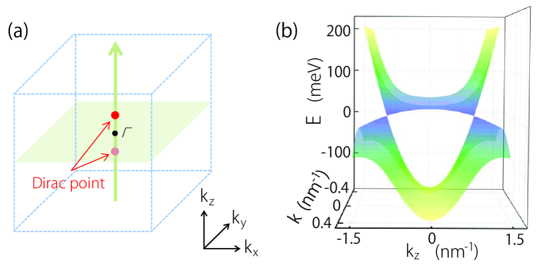
where , , and with parameters to reproduce the band inversion feature. The parameters , and can be obtained by fitting the ab initio result for a specific material. Energy spectrum of this Hamiltonian can be readily solved and is given by Two Dirac points can be obtained by requiring the square root term on the right hand side to vanish, and they are located at with . The two Dirac points are on the -axis, symmetric about the point (see Fig. 1(a)). Each of them is four-fold degenerate and can be regarded as two overlapping Weyl points with opposite chiralities[8] (represented by the two diagonal blocks in Eq.(1)). One observes that the spectrum is isotropic in - plane but is anisotropic for out-of-plane directions. In Fig. 1(b), we plot the bulk energy spectrum as functions of and wave vector in - plane. One can clearly observe the two Dirac points along -axis around which the dispersion is linear. Both the distribution of the Dirac points and the energy dispersion are highly anisotropic. Here and in the following calculations, we take the model parameters for obtained from the first-principles calculations,[9] namely meV, meV, meV, meV, meV, meV, and meV. This leads to nm-1. These parameters agree well with the recent experimental result[11]. We also tested the parameters for another DSM Cd3As2, which shares qualitatively similar low energy physics as . The essential features discussed below applies to Cd3As2 as well.
0.2 Confinement along horizontal direction.
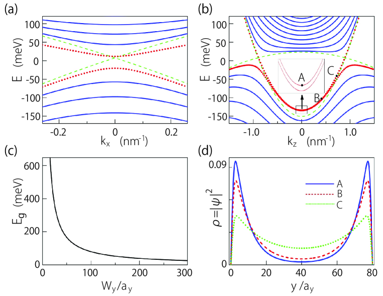
To investigate the quantum confinement effect, we discretize the Hamiltonian on a 3D simple cubic lattice. We take the lattice constants as nm and nm. We first consider the case where the system is confined along one direction. Since the model is isotropic in - plane, in Fig. 2, we choose a finite width along -direction and calculate the system spectrum. Due to the confinement, the continuum spectrum now splits into subbands. This opens up a finite band gap for the bulk at the Dirac points. In Fig. 2(a) and 2(b), we show the energy spectra crossing one Dirac point along and directions respectively. The confinement-induced gap can be clearly observed. The green dashed curves indicate the original bulk bands. One also notice that there exist gapless topological surface states due to the band inversion feature of Hamiltonian (1). These states are marked as red dotted curves. The probability density distribution of three selective states on the surface band is plotted in Fig. 2(d). One observes that these states are indeed peaked around the two surfaces and . Note that because the system has both time reversal and inversion symmetries, hence each point in fact has two degenerate states localized on each surface, and in Fig. 2(d), we choose to plot their symmetric superpositions. The localization of the surface states decreases from with increasing values, as can be seen by comparing the density distribution at different points. Similar to that for the 2D TIs[17], due to the finite width, the states on two surfaces have a small hybridization, which opens a small gap at point, as shown in the inset of Fig. 2(b). Moreover, one can see that the (avoided) Dirac point for the surface states are buried in the valence band. As a result, there are always surface states crossing the bulk confinement-induced gap. This in fact makes the system similar to the usual 3D TI such as Bi2Te3[23]. The surface bands in the gap are protected by time reversal symmetry from opening a gap.
The induced bulk gap depends on the confinement width . Using the quantum well approximation, the effective wave vector for the first few quantum well modes have with . Because the Dirac points are located along -axis and the dispersion around them are linear, the induced gap should roughly scale with as . This feature is indeed confirmed as in Fig. 2(c), where we plot the bulk confinement-induced gap as a function of . The gap shows a monotonic decay with increasing .
0.3 Confinement along vertical direction.
Next, we consider the system with only confinement along -direction. In this case, because the two Dirac points projects to the same point on the surface, there is no topological surface state on the and sufaces. The bulk subbands is isotropic in the - plane, resembling that in Fig. 2(a), and the situation seems quite trivial. However, if we again plot the confinement induced gap versus the confinement width , we observe that in contrast to the case in Fig. 2(c), now the gap has a periodic modulation with a period of superposed upon the power law decay (see Fig. 3(a)). To understand this interesting feature, we note that the two Dirac points are located at finite distance from the point along -axis. The minimum of the gap occurs around the Dirac points. With increasing width , the wave vector of each subband is decreasing and is going to sweep across the Dirac point, leading to a dip on the curve of . Using quantum well approximation for the effective wave vector of subbands , one can easily find that the period of the oscillation should be , which nicely explains the observation in Fig. 3(a). To further confirm this physical picture, we check the density distribution of the band edge states corresponding to the dips labeled in Fig. 3(a). As shown in Fig. 3(b), we see that for a sequence of dips, the corresponding density distributions show increasing number of nodes along the confinement direction, indicating that the states are from subbands with increasing quantum well mode number , which is consistent with our analysis.
Because band inversion occurs for between the two Dirac points, the band gap for a subband is inverted if its is less than . If we consider the system confined along -direction as a quasi-2D system, then the periodic modulation we discussed before is also accompanied with an oscillation in its topological invariant[10]. With increasing , for each quantum well subband with crossing , it adds a to the total 2D number, leading to the oscillation its topological property. Specifically, from Fig. 3(a), we mentioned that the quantum well subband passes around the thickness at point D, the subband passes around point E, and so on. For the thickness at point H, no subband has band inversion, hence the 2D invariant must be zero. For thickness between D and E, one subband becomes topological nontrivial, hence . For thickness between E and F, one more subband becomes nontrivial, leading to a total , i.e. the system again becomes trivial. The oscillatory behavior in topological character for Na3Bi was briefly mentioned in Ref. 9, and a more detailed discussion was presented for Cd3As2 in Ref. 10. Our results are consistent with these previous studies.
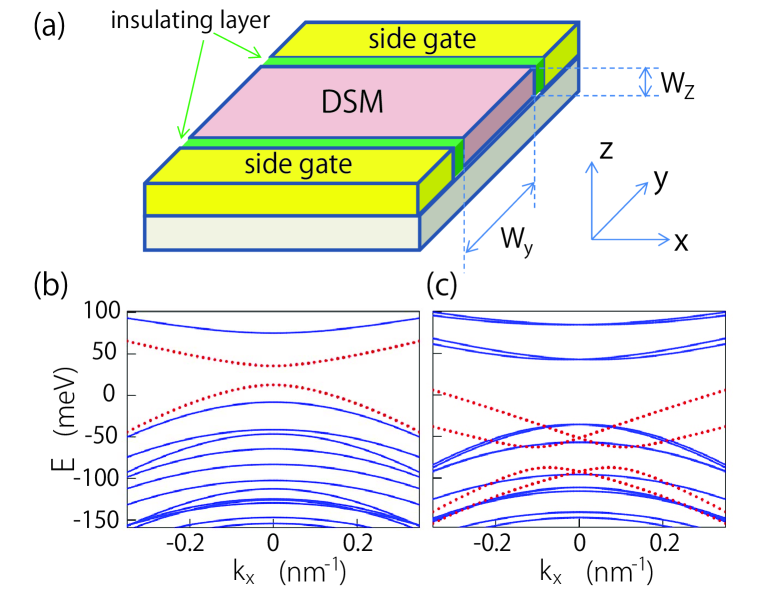
The oscillation in invariant can be better visualized by considering the system confined in both and directions. In Fig. 4, we plot the spectra for the three thickness labeled by H, I, and J in Fig. 3(a), with a width . For point H, since all the subbands are trivial, there is no edge states on the side surfaces and . For point I, one subband becomes nontrivial, as a result, there is a pair of spin-helical edge states on the side surfaces, as indicated by the red dotted curves in Fig. 4(b). One notes that there is a small gap opened at for the edge bands, which is due to the hybridization between the states on the two side surfaces. Note that because the (avoided) Dirac point of the edge bands is buried in the valance bands (at least for Na3Bi and Cd3As2). There are always gapless topological edge states traversing the confinement-induced bulk gap. These states are protected by time reversal symmetry and forming dissipationless edge transport channels. For point J, two subbands have band inversion, each resulting in a pair of helical edge states. Hence in the spectrum, we observe that there are two pairs of helical edge states. Because now scattering between states from different pairs are allowed by symmetry, these edge states lose the topological protection hence are not as robust as that in Fig. 4(b).
0.4 Electric control of boundary channels.
We have analyzed the confinement induced bulk gap, and also show that robust topological boundary channels can exist inside the bulk gap. These channels could be utilized for designing topological devices. For device applications, it is desirable to have full electric control because electric control generally has fast response, consumes less energy, and is more easily to be implemented and integrated. In the following, we investigate the possibility to control the boundary states of confined DSM through electrostatic means.
We first discuss the case by using electric gating on the side surface to tune the surface potential. Let’s consider a nanostructure confined in both and directions with a nontrivial 2D invariant as that in Fig. 4(b). We model the surface potential by gating by applying an equal onsite potential in the lattice model for the two surface layers at and . Because the boundary states are localized near the two side surfaces, they are most susceptible to the applied surface potential than the bulk states. As a result, we could tune the position of the boundary states relative to the confined-induced bulk gap. In Fig. 5(a), a surface potential of V is applied, and we see that the (avoided) edge band Dirac point is shifted into the bulk gap. If the Fermi level is inside both the bulk gap and the surface gap, the transport through the system could be turned off. This means that we could turn the edge transport on and off electrically, which is much desired for application purpose.
When the two gates are at different potential, a transverse electric field along -direction could be applied to the system. This obviously breaks the inversion symmetry. Therefore the double degeneracy is going to be lifted. Here we model the transverse field as a simple linearly varying onsite potential term . As shown in Fig. 5(b), both the bulk subbands and the boundary states have a Rashba type spin splitting induced by the electric field. We have analyzed the spin polarizations of these states and the spin texture indeed coincides with that for Rashba spin-splitting. This result is analogous to the situation discussed in the context of 2D TIs[24]. These spin-polarized edge channels will be useful for spintronics applications. We mention that the modeling of electrostatic effects above is based on a very simple modeling. For more realistic analysis, one needs to solve the electronic structure combined with Poisson’s equation self-consistently. Nevertheless, the essential features we discussed above should still apply.
Discussion
We have shown that the confinement effect generally opens up a gap at the Dirac points, which would be desired for the purpose of designing logical devices. In previous studies of 2D and 3D topological insulators, one aim is to realize robust gapless topological edge or surface states in the bulk gap, which can be used for energy-efficient charge or spin transport. However, it has been found that due to confinement, the states on the opposite edge or surfaces can hybridize and this opens up a gap for the boundary states[17, 18]. In typical 2D TIs such as HgTe/CdTe quantum wells, the edge state crossing occurs in the bulk gap. Hence when a gap is opened by coupling between the two edges, the edge channels would no longer be gapless. This was considered as a detrimental effect for applications[17, 24]. In this regard, the DSM nanostructures is in fact advantageous in that its edge state crossing is buried in the valence band hence the edge transport inside bulk gap would not be affected (at least for the cases of Na3Bi and Cd3As2). As a result, there are always gapless topological edge channels in the confinement-induced bulk gap which are protected by time reversal symmetry. This implies that the DSM nanostructures could offer a better platform for designing topological electronic devices with low power dissipation. Note that the above comparison is made in the native states of the systems. We also mention that the detailed edge states dispersions would depend on the edge/surface condition. For example, the edge sates could be shifted in energy by electric gating as we shown in the previous discussion, and be distorted by surface defects or doping[13].
To conclude, we have investigated the electronic properties of confined DSM nanostructures. We find that the quantum confinement effect is strongly anisotropic. The confinement generally induce a bulk gap at the Dirac points and it shows a periodic modulation when the confinement is along -axis. This modulation is accompanied with topological transitions. For a topological nontrivial state, we point out that the system is in fact superior to usual 2D TIs in terms of robust gapless edge transport. Electric means to manipulate the edge channels are discussed. Our result show that DSM nanostructures offer a promising platform for designing novel topological quantum devices.
Methods
0.5 Lattice model.
To investigate the confinement effects, we discretize the low energy continuum model in Eq.(1) on a 3D tetragonal lattice with lattice constants , and along the three orthogonal directions.
| (2) |
where is the creation (annihilation) operator for an electron on the site . The on-site matrix element is given by
| (3) |
where . The ’s and ’s (and the below) are the material specific parameters defined in the main text. The nearest-neighbor hopping matrix elements , and are given respectively as
| (4) |
| (5) |
and
| (6) |
The electrostatic effects are modeled by adding an on-site electrostatic potential energy . Using this lattice Hamiltonian, the low energy spectrum and the wavefunctions of electronic states for the DSM nanostructures can be obtained conveniently.
References
- [1] Hasan, M. Z. & Kane, C. L. Colloquium: Topological insulators. Rev. Mod. Phys. 82, 3045-3067 (2010).
- [2] Qi, X. L. & Zhang, S. C. Topological insulators and superconductors. Rev. Mod. Phys. 83, 1057-1110 (2011).
- [3] Knig, M. et al. Quantum Spin Hall Insulator State in HgTe Quantum Wells. Science 318, 766-770 (2007).
- [4] Ando, Y. Topological Insulator Materials. J. Phys. Soc. Japn. 82, 102001 (2013).
- [5] Murakami, S. Phase transition between the quantum spin Hall and insulator phases in 3D: emergence of a topological gapless phase. New J. Phys. 9, 356 (2007).
- [6] Wan, X. et al. Topological semimetal and Fermi-arc surface states in the electronic structure of pyrochlore iridates. Phys. Rev. B 83, 205101 (2011).
- [7] Burkov, A. A. & Balents, L. Weyl Semimetal in a Topological Insulator Multilayer. Phys. Rev. Lett. 107, 127205 (2011).
- [8] Young, S. M. et al. Dirac Semimetal in Three Dimensions. Phys. Rev. Lett. 108, 140405 (2012).
- [9] Wang, Z. J. et al. Dirac semimetal and topological phase transitions in (A = Na, K, Rb) Phys. Rev. B 85, 195320 (2012).
- [10] Wang, Z. J. et al. Three-dimensional Dirac semimetal and quantum transport in . Phys. Rev. B 88, 125427 (2013).
- [11] Liu, Z. K. et al. Discovery of a Three-Dimensional Topological Dirac Semimetal, . Science 343, 864-867 (2014).
- [12] Zhang, Y. et al. Molecular beam epitaxial growth of a three-dimensional topological Dirac semimetal . Appl. Phys. Lett. 105, 031901 (2014).
- [13] Liu, Z. K. et al. A stable three-dimensional topological Dirac semimetal Cd3As2. Nat. Mater. 13, 677 (2014).
- [14] Borisenko, S. et al. Experimental Realization of a Three-Dimensional Dirac Semimetal. Phys. Rev. Lett. 113, 027603 (2014).
- [15] Neupane, M. et al. Observation of a three-dimensional topological Dirac semimetal phase in high-mobility . Nat. Commun. 5, 3786 (2014).
- [16] Yi, H. M. et al. Evidence of Topological Surface State in Three-Dimensional Dirac Semimetal . Sci. Rep. 4, 6106 (2014).
- [17] Zhou, B. et al. Finite Size Effects on Helical Edge States in a Quantum Spin-Hall System. Phys. Rev. Lett. 101, 246807 (2008).
- [18] Linder, J., Yokoyama, T. & Sudb, A. Anomalous finite size effects on surface states in the topological insulator . Phys. Rev. B 80, 205401 (2009).
- [19] Zhang, Y. et al. Crossover of the three-dimensional topological insulator to the two-dimensional limit. Nat. Phys. 6, 584-588 (2010).
- [20] Lu, H. Z. et al. Massive Dirac fermions and spin physics in an ultrathin film of topological insulator. Phys. Rev. B 81, 115407 (2010).
- [21] Liu, C. X. et al. Oscillatory crossover from two-dimensional to three-dimensional topological insulators. Phys. Rev. B 81, 041307 (2010).
- [22] Imura, K. I. et al. Finite-size energy gap in weak and strong topological insulators. Phys. Rev. B 86, 245436 (2012).
- [23] Zhang, H. J. et al. Topological insulators in , and with a single Dirac cone on the surface. Nat. Phys. 5, 438-442 (2009).
- [24] Liu, G. H., Zhou, G. H. & Chen, Y. H. Effect of transverse electric field on helical edge states in a quantum spin-Hall system. Appl. Phys. Lett. 99, 222111 (2011).
This work was supported by NSFC (Grant Nos. 11264019, 11364019, 11464011 and 11274108), by the development project on the young and middle-aged teachers in the colleges and universities in Jiangxi, and by SUTD-SRG-EPD2013062.
X.X. and S.A.Y. conceived the idea. X.X. performed the calculation and the data analysis. X. X., S.A.Y., and G.H.Z. contributed to the interpretation of the results and wrote the manuscript. Z.F.L. and H.L.L. contributed in the discussion. All authors reviewed the manuscript.
The authors declare no competing financial interests.
Correspondence and requests for materials should be addressed to Shengyuan A. Yang or Guanghui Zhou.