subref \newrefsubname = section \RS@ifundefinedthmref \newrefthmname = theorem \RS@ifundefinedlemref \newreflemname = lemma
Synchronization of pairwise-coupled, identical, relaxation oscillators based on metal-insulator phase transition devices: A Model Study
Abstract
Computing with networks of synchronous oscillators has attracted wide-spread attention as novel materials and device topologies have enabled realization of compact, scalable and low-power coupled oscillatory systems. Of particular interest are compact and low-power relaxation oscillators that have been recently demonstrated using MIT (metal-insulator-transition) devices using properties of correlated oxides. Further the computational capability of pairwise coupled relaxation oscillators has also been shown to outperform traditional Boolean digital logic circuits. This paper presents an analysis of the dynamics and synchronization of a system of two such identical coupled relaxation oscillators implemented with MIT devices. We focus on two implementations of the oscillator: (a) a D-D configuration where complementary MIT devices (D) are connected in series to provide oscillations and (b) a D-R configuration where it is composed of a resistor (R) in series with a voltage-triggered state changing MIT device (D). The MIT device acts like a hysteresis resistor with different resistances in the two different states. The synchronization dynamics of such a system has been analyzed with purely charge based coupling using a resistive () and a capacitive () element in parallel. It is shown that in a D-D configuration symmetric, identical and capacitively coupled relaxation oscillator system synchronizes to an anti-phase locking state, whereas when coupled resistively the system locks in phase. Further, we demonstrate that for certain range of values of and , a bistable system is possible which can have potential applications in associative computing. In D-R configuration, we demonstrate the existence of rich dynamics including non-monotonic flows and complex phase relationship governed by the ratios of the coupling impedance. Finally, the developed theoretical formulations have been shown to explain experimentally measured waveforms of such pairwise coupled relaxation oscillators.
With insurmountable challenges facing silicon scaling, research
has started in earnest to identify potential computational architectures
and device technologies for a post-silicon era. One such paradigm
where coupled oscillatory systems perform computational tasks such
as pattern recognition and template matching has garnered recent interest;
and it necessitates the fabrication of compact and scalable oscillators
that can be electrically coupled. Recent advances in the development
of correlated oxides have led to successful demonstration of coupled
relaxation oscillators. Here we investigate the coupling dynamics
of pairwise coupled identical relaxation oscillators based on such
correlated materials that exhibit electrically controlled metal-insulator-metal
phase transitions. Using analytical and numerical techniques we show
how the coupling network can lead to in-phase and out-of-phase locking
as well as create a bistable system. Such systems have already been
shown to offer computational capabilities beyond the traditional Boolean
fabric.
I Introduction
Synchronization of systems of oscillators has attracted widespread attention among physicists, mathematicians and neurobiologists alike. Even simple descriptions of oscillators and their coupling mechanisms give rise to rich dynamics. Synchronization dynamics of coupled oscillators not only have a wide variety of applications in engineering Datta:2014aa ; Shukla:2014aa but they also explain many natural, chemical and biological synchronization phenomena like the synchronized flashing of fireflies, pacemaker cells in the human heart, chemical oscillations, neural oscillations, and laser arrays, to name a few Dorfler:2012aa . Coupled sinusoidal oscillators have been extensively studied Winfree:1967aa , Kuramoto:1975aa ; Kuramoto:2003aa and their application in the computational paradigm has been well demonstratedNikonov:2013aa ; Izhikevich:2000aa . A generalized description of oscillators in these models is usually a canonical phase model Dorfler:2012aa ; Mallada:2013aa , and the coupling mechanisms is generally assumed weak and composed of simple periodic functions. Several studies on more general periodic coupling functions have been studied Acebron:2005aa . Along with sinusoidal oscillators, non-linear Van-der-Pol oscillators and several of its variants have also been studied and the applicability of such models in neurobiological and chemical oscillators have been demonstrated Rand:1980aa ; Storti:1982aa ; Kouda:1982aa ; Chakraborty:1988aa . Such analytic models of coupled oscillatory systems almost always require a canonical phase description of the oscillators and a periodic phase dependent additive coupling that can be classified as weak. Although such a description of a system of oscillators is elegant and provide key insights, relaxation oscillators that have recently been demonstrated using phase transition MIT devices, cannot be modeled using such a simple phase description. Prior work by the authors have experimentally demonstrated locking and synchronization in a pairwise coupled system of relaxation oscillators Shukla:2014aa and its possible application in computation has also been discussedDatta:2014aa . The coupling behavior of relaxation oscillators illustrate complex dynamical properties Saito:1988aa and in this paper we study the synchronization behavior of a pair of identical and electrically coupled relaxation oscillators Shukla:2014aa . Individual oscillators are composed of either two MIT devices in series (D-D configuration) or a MIT device in series with a linear resistor (D-R configuration) Shukla:2014aa and electrical coupling is enabled through a parallel connected R-C network. We show, through analytical and numerical techniques how the final steady state relative phase of such coupled oscillators depend on the coupling function. For certain range of values of the coupling function, we note the possibility of a bistable system, where both in-phase and out-of-phase locking are stable, thereby giving rise to the possibility of using such oscillatory networks in computation Izhikevich:2000aa ; Datta:2014aa .
II Electrical Circuit Model and Representation
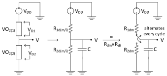
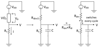
An electrical circuit representation of the relaxation oscillators is important to define the form of coupling which is physically realizable. The basic relaxation oscillator involves repeated charging and discharging of a capacitor through a resistive path. Switching between charging and discharging has to be done autonomously by the circuit configuration. In this paper, we are concerned with the relaxation oscillators built using state-changing devices. Such state-changing devices are fabricated using correlated oxide (vanadium dioxide, ) and exhibit MIT (metal-insulator transition) where the device switches between a metallic and an insulating state under the application of heat or an electric fieldKar:2013aa . Further details about the physical implementation of these devices are discussed in section VIII. We will consider two kinds of relaxation oscillator circuits using such state-changing devices - (a) two state-changing devices in series (1). We will refer to this configuration as D-D. And (b) a state changing device in series with a resistance (2)Shukla:2014aa . This configuration will be referred to as D-R. The D-D configuration is enticing in its simplicity, both in physical realization and analysis as will be evident in the following sections. The D-R configuration, on the other hand, has already been experimentally demonstrated Shukla:2014aa and can be thought of as an extension of the D-D configuration albeit with more complex dynamics of synchronization. In this paper we will first study the D-D configuration, using analytical and numerical techniques; and show through phase models and flow analysis some key results in the D-R configuration.
The state transition of the device follow:
-
(a)
Only the resistance of the device changes with its state; and the resistance is linear;
-
(b)
A state transition is triggered by the voltage across the device. This triggering can be electric field driven or thermally driven, and can be modeled as an equivalent triggering voltageShukla:2014aa . When the voltage exceeds a higher threshold , the state changes to a metallic (low resistance) state and when the voltage exceeds a lower threshold , the state switches back to the insulating (high resistance) state. The thresholds and are not equal, i.e. there is hysteresis in the switching with , and
-
(c)
A capacitance is associated with the device that ensures gradual build up and decaying of the voltage (and hence energy) across the device .
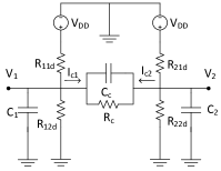
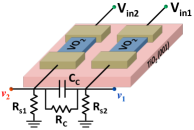
The present study of the synchronization dynamics of such coupled systems, although inspired by the experimental realization of based oscillators, is not limited to these oscillators only, but encompasses a class of similar pairwise-coupled relaxation oscillators as well. The circuit equivalents of single and coupled relaxation oscillators are shown in 1, 2 and 3 respectively. The internal resistance of the device has two different values in the two states of the device - in the insulating (high resistance) state and in the metallic (low resistance) state. is the internal capacitance of the MIT device (including any parasitic capacitances) and is the series resistance. We will also assume that . In the D-D configuration, the capacitor being charged can be represented as a single capacitor at the output circuit node. The coupling circuit is a parallel combination of a capacitor and a resistor . As shown, the output node of the oscillator is between the device and the resistance, and the coupling circuit is connected between these output nodesShukla:2014aa .
III Model Development For Isolated & Coupled Oscillators
Before investigating the system dynamics, let us establish the system model and the system of ODEs that define the system. This will allow us to define the conditions for oscillation as well as the coupling dynamics. We will first consider D-D configuration and then D-R configuration as an extension of the D-D configuration. The D-D configuration, owing to its inherent symmetry renders to easier dynamics and analysis and provides valuable insights into the system. Such key numerical and analytical results for this are discussed in the following sections.
III.1 D-D configuration
The circuit equivalent for a D-D type relaxation oscillator is shown in 1. For simplicity, all voltages are normalized to (including and ). We define conductances , and . For the conductances, subscript denotes a state dependent device conductance and denotes metallic/insulating state respectively. The subscripts preceding or refer to the corresponding numbered device as shown in figure. Also, it is assumed that , which means that the state essentially disconnects the circuit. This implies that the effective charging happens through and effective discharging through . The single D-D oscillator can be described by the following set of piecewise linear differential equations:
| (1) |
where is the lumped capacitance of both devices along with the parasitics. The equation can be re-written as:
| (2) |
where denotes the conduction state of the device (0 for metallic, and 1 for insulating) and and depend on the device conduction state as follows:
| (3) | |||||
| (4) |
When two identical oscillators are coupled in a manner described in 3, the system can be described by the following coupled equations:
| (5) | ||||
| (6) |
where and are the lumped capacitances of the oscillators. For conductances , the first subscript denotes the oscillator and the second denotes the device. is the coupling current given by:
| (7) |
When coupled, the system has 4 conduction states corresponding to the 4 combinations of and . Analogous to (2), the coupled system can be described in matrix form as:
| (8) |
where is the state variable at any time instant . The matrices and , and vector are given by:
| (9) |
| (10) |
Here, is the ratio of the combined lumped capacitance of oscillator to the coupling capacitance , and is the ratio of the metallic state resistance of device of oscillator, where and . The fixed point in a conduction state is given by and the matrix determining the flow (the flow matrix or the velocity matrix) is given by as can be seen in (LABEL:main-1). In section V we analyze the steady state locking and synchronization dynamics of two such identical oscillators coupled with a parallel resistive and capacitive element as shown in 3.
III.2 D-R configuration
The equivalent circuit for a D-R type relaxation oscillator is shown in 2. As in the case of D-D configuration, voltages are normalized to . The conductances involved are , , and . Effective charging happens through as in the previous case but there is an added leakage through , whereas effective discharging happens only through . Following the same methodology as in the D-D case, the equation for the single D-D oscillator dynamics can be written as:
| (11) |
which can be re-written as:
| (12) |
where,
| (13) | |||||
| (14) |
and denotes the conduction state of the system as before. In case of coupled D-R oscillators, arguments similar to the previous case lead to the same matrix equation as (8):
| (15) |
where matrices and remain the same as before but matrix changes to the following:
| (16) |
| (17) |
Here and .
For all numerical simulations in the rest of the paper, the normalized values of and w.r.t are chosen to be 0.2 and 0.8 respectively.
IV Phase Space, Flows and Oscillation Conditions
IV.1 Single Oscillators
A series arrangement of two MIT devices (D-D), or an MIT device and a resistor (D-R) will oscillate only when certain conditions are met. In case of two devices in series (D-D), the two devices must be in opposite conduction states (one metallic and the other insulating) all the time for oscillations to occur. If the threshold voltages and are same for the devices and the following condition holds
| (18) |
and at the devices are in different conuduction states, then any time one device switches, the other will make the opposite transition as well. The basic mechanism of oscillations is as follows. The device in metallic state connects the circuit and charges (discharges) the output capacitor, and the other device in insulating state does not participate in the dynamics. As the capacitor charges, the voltage drop across the device in metallic state decreases and crosses the lower threshold . At the same instant, the voltage drop across the other device in insulating state increases and crosses the higher threshold because . The devices then switch states and the cycle continues. The devices can be conceived as a switch which is open in insulating state (ignoring any leakage in the insulating state) and closed in metallic state (1). If and deviate from (18), the devices will not switch at the same instant and oscillations will stop as the system settles to a stable point where both devices are in same state and the voltage of the output nodes remains at . This may require additional startup circuit in the system, which is trivial to integrate.
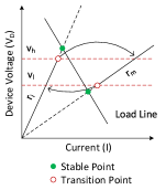
In D-R configuration, another set of conditions have to be metHu:1986aa which depend on the relative values of the device resistances in the two states ( and ) and the series resistance (). These conditions can be described using the phase diagram of the MIT device 4. Lines with slopes and are the regions of operation of the device in insulating and metallic states respectively. The intersection of these lines with the load line due to the series resistance gives the stable points of the system in the two states. For self-sustained oscillations, the stable points in each state should lie outside the region of operation, i.e. outside the region defined by horizontal lines passing through the transition points. This ensures that the system always tries to reach the stable point in the current state but is always preceded by a transition to the other state. This moves the system towards the stable point of the other state (away from the previous stable point) and hence the system never reaches any stable point and oscillates. This configuration is robust towards deviation of and from condition (18) and as only one device is involved, it does not require the difficult constraint of simultaneous switching of devices as was in the D-D case. This reduced requirement of symmetry is an attractive property of the D-R configuration as initial experiments have confirmed sustained oscillations in this configurationShukla:2014aa .
We define the region of operation of a device (and hence of an oscillator) as the region where the device voltage lies between and (or the output voltage lies between and ). For the D-D case, the oscillators are expected to remain within the region of operation all the time. However in the D-R case, the system can go outside the region of operation in a specific manner as described later.
IV.2 Coupled Oscillators
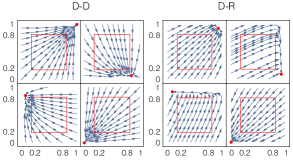
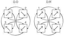
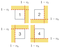
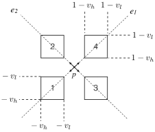
For analyzing the coupled circuits, the phase diagram of a coupled system can be drawn in the space as was done in 4. However, we note that in a given conductio state of the system, , can uniquely identify the system, and hence, space is sufficient for a phase diagram. Therefore, we can draw 4 different phase diagrams of the system for each conduction state (5) with transitions among themSaito:1988aa (6). The transitions occur at the edges when either or reach the higher or lower threshold for state change from metallic to insulating or vice versa. The flows in each of the 4 conduction states are linear flows and hence have a single fixed point (5). The conditions for oscillations can be described using 7. Analogous to the case of a single oscillator, these stable points should lie outside the region of operation (in the shaded region) in a way that the system always tries to move towards these stable points but should be preceded by a state transition which occurs when the system reaches the (red) dashed lines.
IV.2.1 Monotonic Flows and Periodic Orbits
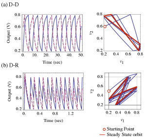
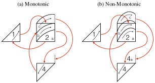
The conditions of 7 are general enough to hold for both D-D and D-R configurations and they ensure that the system does not settle down to a stable point and voltages across oscillators repeatedly increase and decrease. However, these conditions do not ensure the existence of a stable orbit which can give periodic oscillations. To ensure existence of a stable periodic orbit, we consider additional conditions for the systems. For D-D configuration, we consider systems where the flows in the states are monotonic, i.e. and are either constantly increasing or constantly decreasing in the region of operation of any conduction state. \FigrefTransitions show these monotonic directions with the state transitions for D-D coupled oscillator configurations. It is proved later that for two identical coupled D-D oscillators, this condition of monotonicity of the flows is sufficient for existence of a stable orbit and hence for periodic oscillations. For D-R coupled oscillators, we consider systems where either the direction of flows are strictly monotonic as shown in 6 or are non-monotonic in a very specific way as discussed in VII (see 23). In this case, periodic oscillations can be ensured for certain conditions as described in section VII. It should be noted here that in the D-R case, the system can also go outside the region of operation as seen in 8, but if the fixed points lie in the above mentioned shaded regions, the system will always oscillate. \FigrefSimulation-waveforms shows typical time-domain waveforms and corresponding phase-space trajectories for the coupled oscillators of the D-D and D-R types.
V Symmetric D-D coupled oscillator dynamics
Let us first investigate the case when the D-D oscillators are identical and their effective charging and discharging rates are equal, i.e. and . This corresponds to a well designed and ideal oscillator system where the pull-up and pull-down device resistances have been matched to create equal charging and discharging rates. In such a scenario the velocity matrices in the four conduction states become equal. As such, the state spaces in the four conduction states can be represented in a common state space with the system flow described by the common velocity matrix and a single fixed point. However, in this common state space, the regions of operation in the four conduction states will be four distinct regions. The position of these regions for a conduction state would depend on the position of its respective fixed points in the original state space. Such a combined phase space is shown in 9.

The symmetry of the system is apparent in the flow as well. The eigen values and eigen vectors of the velocity matrix of the symmetric system are
| (19) |
| (20) |
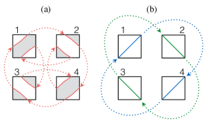
Real negative eigen values imply that the flow of the system is symmetric about both the eigen vector directions (i.e. a mirror image of itself about the eigen directions) as shown in 10. The stable fixed points in the conduction states 1(00), 2(01), 3(10) and 4(11) are , , and respectively. Hence, the line along the eigen vector is the diagonal for both conduction states 1 and 4. Under the assumption that the normalized thresholds and are symmetric i.e. , the line along also becomes the diagonal for states 2 and 3. This is because the fixed points of conduction states 2 and 3 - and lie on line in their original state spaces which is same as the eigen direction . It should now be noted that the transitions between the conduction states, the regions of operation and the flow, all have the same common discrete symmetry - mirroring about and . We can do a symmetry reduction at this point and the system can be completely described by just two states and two transitions (11a).
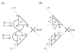
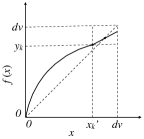
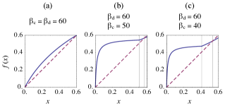
To study the steady state periodic orbits of this system, we calculate the return map on the left edge of state 1 in 11a which is . In this case, any periodic orbit in the symmetry reduced space will correspond to at least one periodic orbit in the complete space (see 13). Also, if no fixed point exist in the symmetry reduced space, then there is definitely no periodic orbit in the complete space. The coordinate measurements on the edges are defined as shown in 11b. is the mapping from the left edge of state 1 to its top edge and is the mapping from left edge of state 2 to its bottom edge. and are defined on their respective edges as shown in 11b. As both the eigen values and are real and negative, will lie above line and will lie below it. A representative plot of , and (i.e. the return map ) is shown in 12 where . The composition lies above if is more curved than and vice versa. As the return map is always increasing, only the first return map needs to be considered for finding fixed points and the higher return maps don’t add new fixed points. When the coupling is more capacitive, the composition function tends to be concave as shown in 12a. Proposition 1 gives a mathematical form to this notion.

If the system moves from any arbitrary point on the flow, say to another point, in time then the following implicit equation can be written:
| (21) |
In state 1, lies on the left edge and lies on the top edge. To define we substitute in (LABEL:flow-equation) and obtain an implicit equation for as:
| (22) |
Similarly, an implicit equation for can be written as:
| (23) |
where .
Proposition 1 : Sufficient condition for out-of-phase
locking: For , i.e.,
the coupled symmetric and identical system has only two steady state
locking orbits - in-phase and out-of-phase. Further, the in-phase
locking is unstable and the out-of-phase locking is stable.
Proof : The proof can be divided in two steps - (a) There are only two fixed points of - at 0 and at , and (b) and which implies that the in-phase locking is unstable and anti-phase locking is stable.
The first part is proved as follows.
As and are negative, and . And as , and . Also implies . This gives us the following inequalities:
| (24) | |||||
| (25) |
where the equality holds at the end points i.e. at and for (24) and at and for (25). At any fixed point for the return map , and and equations (24) and (25) should be consistent with these fixed point equations. Substituting and in (24) and (25) we get:
| (26) | |||||
| (27) |
These equations are consistent only when
| (28) |
which in turn can be true only at the end points, i.e. or , because . It can be confirmed that this is indeed the case by inspection of 11.
The second part of the proof is proved by calculating . and are calculated from (22) and (23) as:
| (29) | |||||
| (30) |
where and . Also implies . Hence
| (31) |
And as has no other fixed points between 0 and and
is continuous, . Hence, proved.
It should be noted that this condition is not a strict bound but rather provides key design insights when a particular form of coupling (anti-phase) is soughtDatta:2014aa .
V.1 Capacitive, Resistive Coupling and Bistable Orbits
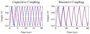
The two extreme cases of purely resistive and purely capacitive coupling are of interest. In case of coupling using only a capacitor, the symmetric and identical coupled system always has a stable anti-phase and an unstable in-phase locking. This is because in case of purely capacitive coupling, and so for all finite . Even in practical cases where some parasitic resistance is included in parallel with the coupling capacitor Shukla:2014aa , is typically much larger than . Such anti-phase locking matches well with recent experimental findings of capacitively MIT coupled oscillators as discussed in Datta:2014aa . In case of coupling using only a resistor, the symmetric and identical coupled system will have a stable in-phase and an unstable anti-phase orbit, as can be predicted from 15 for . Time domain simulations of the coupled systems with purely capacitive and purely resistive coupling are shown in 14. The parameter values for capacitive coupling are and and those for resistive coupling are and .
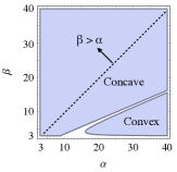
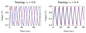
dd-sym-return-maps (b and c) show cases when . In the intermediate case when the return map transitions from concave to convex, the system goes through a state where both in-phase and anti-phase locking are stable with one unstable fixed point in between (12b). In 15 the two regions for concave and convex return map can be clearly seen. They are separated by a thin region which represents the case of bistability. \Figrefdd-sym-bistable-waveforms shows the time domain simulation waveforms of oscillator outputs for and . We note that the initial voltage of the first oscillator is 0.2V and depending on the initial voltage of the second oscillator, the system can either lock in phase or out of phase. These design parameters correspond to a bistable system of the kind shown in 12b, and hence the final steady state locking is in-phase or out-of-phase depending on the initial phase of the system. When the initial phase (or output voltage) of oscillators are close to each other (represented by gray region in 13a) the system locks in-phase, and when they are far the system locks out-of-phase for the same circuit parameters.
VI Asymmetric D-D coupled oscillator dynamics
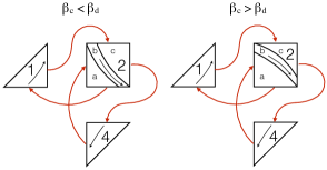
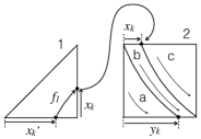
Let us now investigate the case of D-D oscillator dynamics where the two oscillators are identical but the pull-up and pull-down devices are non-identical thereby giving rise to asymmetric charging and discharging rates. As the the oscillators are identical, and where subscripts and stand for charging and discharging. The symmetry of the system (due to the identical oscillators) can be seen in the flows of the states. Flows of conduction states 1(00) and 4(11) are mirror images about the diagonal and the flow in conduction state 2(10) is equivalent to the flow in state 3(01) with axes x and y interchanged. This symmetry is also shown in the transitions between states. The system can be expressed after reducing the symmetry as in 17. For , two kinds of cycles are possible in the regions and . To find the fixed points of the system, we draw the return map with the bottom edge of state 1 as the Poincare section. Because it is a symmetry reduced space, we consider the first return map for trajectories of the type and the second return map for trajectories of the type . Let as shown in 18 where is the mapping from bottom edge of conduction state 1 to its right edge, and and are the mappings between edges in conduction state 2 as shown. Then the return map is given by:
| (32) |
Proposition 2 : Existence of stable periodic orbit
in asymmetric D-D coupled oscillator system: If is the return
map for the D-D asymmetric coupled oscillator on the bottom edge of
state 1 then the following are true:
-
(a)
is continuous
-
(b)
for and
-
(c)
has one fixed point at 0 and at least one in the interval at, say,
-
(d)
Either the fixed point at is stable, or there exists a stable fixed point at where
Proof : (a) The return map is separately continuous in intervals and as it is a composition of mappings of continuous flows. The continuity of at can be established by considering two points close to on either side. From (32) we can see that , and hence is continuous at .
(b) It can be proved by similar procedure as adopted before in Proposition 1 that for and .
(c) The fixed point at 0 can be seen clearly in the flow diagram. In interval , the fixed points of first return will also be the fixed points of second return (which is ), but not the other way around. Now and . As is continuous, and hence decreasing, in the interval , there exists a fixed point for , and hence for , in the interval .
(d) As is continuous and has fixed points at and ,
one of these two should be stable if there is no other fixed point
in between and . If they both are unstable, then a stable
fixed point exists in the interval . Hence proved.
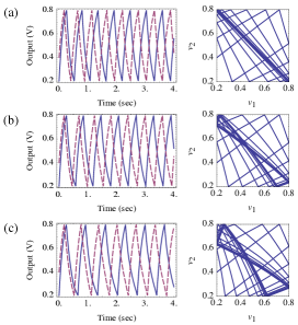
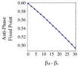
dd-asym-return-map shows a representative return map for the asymmetric D-D configuration. The poincare section chosen in the symmetric D-D case was the left edge of conduction state 1. Due to symmetry, the left edge of conduction state 1 is same as the bottom edge of conduction state 1. Hence the return maps in the symmetric D-D case can be compared with the return maps in the asymmetric D-D case as if they were drawn on the same edge. \Figrefdd-sym-asym-return-maps shows a comparison of the return maps of a symmetric case with that of two asymmetric cases . The corresponding time domain waveforms and phase plots are shown in 20. The figure clearly shows that the steady state periodic orbit changes from a diagonal (perfect anti-phase locking) to a butterfly shaped curve (imperfect anti-phase locking) as the asymmetry increases. However, the time domain waveforms for butterfly shaped periodic orbits would still be very similar in appearance to anti-phase locking. The fixed point close to in the return map shifts away from as the difference between and increases. This trend can be seen in 22 which shows the movement of the anti-phase fixed point with for fixed and . For , the cycles will be of the type and , and the return map will have to be drawn on an edge of state 4. The return map in this case will be analogous to the case with and interchanged.
VII D-R coupled oscillator dynamics
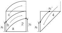
In this section we consider the dynamics of a D-R coupled system. This is of interest because of its ease of fabrication, relaxed conditions for oscillations and already published reports of such coupled oscillatory systems Shukla:2014aa . We consider coupling of identical oscillators and hence we define and . Unlike the D-D coupled oscillator case, the notion of symmetric charging and discharging does not apply in D-R coupled oscillator case because the circuit by construction is different for charging and discharging. During charging a part of the net charging current charges up the output capacitor whereas the rest of it flows through the pull-down resistance to ground. The process of discharging has no such leakage component. In terms of the conductance ratio , this can be explained by the fact that the net charging component in the matrix A is () and it is always greater than the discharging component . However, the flows can still be simplified for analysis as was described in section IV. The simplification assumes that the flows are monotonic in the regions of operation in all four conduction states, but the direction of monotonicity is different from the D-D coupled oscillator case as shown in 6. For our analysis, a particular type of non-monotonicity is allowed in state 2 (and state 3) as shown in 23. Here the fixed point for conduction state 2 satisfies the condition of oscillation shown in 7, but the flow in state 2 as shown in the symmetry reduced space (23) is non monotonic. We will consider the case of identical oscillators , and following the methodology of the asymmetric D-D case, we can reduce the symmetry of identical oscillators as shown in 23. In this case, two kinds of cycles are possible - and . To find the fixed points of the system, we draw the return map on the top edge of conduction state 4 as the Poincare section. Because it is a symmetry reduced space, we will have to consider the second return map for cycles of the type but only the first return map for type cycles. Let be the mapping from top edge of state 4 to its left edge, be the mapping from the extended right edge of state 4 to its top edge, , and be the mappings between edges of state 2, and as shown in 24. Then the return map is given by:
| (33) |
Proposition 3 : Conditions for existence of stable
periodic orbit in D-R coupled oscillator system: If is the return
map for the D-R coupled oscillator system on the top edge of state
4 in the symmetry reduced state space (23)
then
-
(a)
is piece-wise continuous with discontinuity at . Moreover, and .
-
(b)
has at least one fixed point in the interval at, say,
-
(c)
If , has at least one stable fixed point in the interval
Proof : (a) The argument is the same as in Proposition 2. The return map is separately continuous in intervals and as it is the composition of continuous flows. From (33) we can see that and .
(b) In the interval , the fixed points of the first return map will also be the fixed points for its second return map (which is ). Now and . As is continuous (and hence decreasing) in this interval, there exists a fixed point for , and hence , in the interval .
(c) As , is continuous in the interval
and has a fixed point at where , hence
either the fixed point at is stable or there exists another
fixed point in the interval which lies in .
Hence proved.
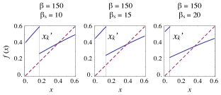
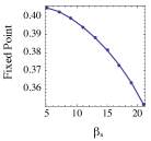
dr-return-maps shows the return map on the top edge of state 4 for the D-R coupled oscillator system for varying . The return maps in the figure have a single stable fixed point at in the interval . The movement of the fixed point with is shown in 26.
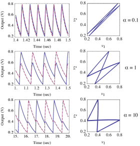
Another important design consideration for the coupled oscillator system, is the role of the coupling circuit on the overall system dynamics, as is seen in 27. We note that as the value of increases the phase diagram in the plane shows strong sensitivity. In particular, for low values of , the system shows in-phase locking. As increases (for intermediate value of ), the butterfly shaped phase plot widens and the system exhibits a non-monotonic decrease in the output voltages, and from to . This can also be seen in the time domain waveforms where the output voltages first decrease to an intermediate voltage, then increase and again decrease; clearly demonstrating four possible conduction states (MM, MI, IM and II) in both phase and time domain plots. Finally, for high values of the butterfly in the phase plot opens even further, thus making the decrease of output voltages from to more monotonic and the system tends to anti-phase locking, as exhibited in both phase and time (27).
VIII Experimental verification
An MIT device can be realized using (Vanadium dioxide) which exhibits unique electronic properties like metal-insulator phase transitions. has been shown to undergo abrupt first order metal-to-insulator and insulator-to-metal transitions with upto five orders of change in conductivityLadd:1969aa and ultra-fast switching times Kar:2013aa . Transitions have been shown to be electrically driven, thermally driven or a combination thereof. Recent work shows that for such a transition, a metallic filament structure is formed which acts as a conduction pathway in the low resistance state of Freeman:2013aa . Also, a series circuit of with a resistive pull down network has been shown to exhibit self-sustained electrical oscillationsShukla:2014aa when conditions of oscillations as described above are met. Moreover, two such relaxation oscillators can be electrically coupled to produce synchronized oscillations Shukla:2014aa .
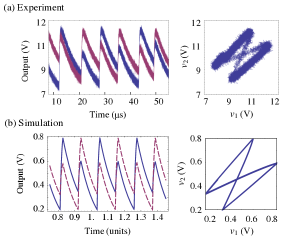
For experimental validation, we apply our models of coupled relaxation oscillators on a system of two coupled oscillators. \Figrefexp-circuit shows a schematic representation of the coupled circuit with a parallel resistance () and capacitance () as the coupling circuit. Frequency domain results of this system have been previously reported Shukla:2014aa showing a close match between experiments and theoretical results of a D-D model; and are not reproduced here. Using the D-R model developed in this paper, we obtain close match in the time-domain and phase plots of the oscillator system as well. With proper calibration of the system parameters, the D-R model described above shows very close qualitative match with experimental results. One such experimental result has been shown in 29 along with model prediction. This validation of the proposed models enables further design of experiments. It further models and explains both qualitative and quantitative the role of the system design parameters on the rich synchornization dynamics.
IX Conclusions
This paper presents a model study of the synchronization dynamics of a pair of identical and electrically coupled relaxation oscillators when physically realized using MIT devices. Experimental realization of such devicesDatta:2014aa ; Shukla:2014aa has motivated the study of their dynamics, with emphasis on phase synchronization, locking conditions and potential programmability of the phase relations using electrical means. We investigate the case of a purely MIT based oscillator (D-D) and that of a hybrid oscillator composed of an MIT device and a passive resistance (D-R configuration). We show through numerical and analytical techniques, validated against experimental results, the existence of out-of-phase locking (in purely capacitive coupling), in-phase locking (in purely resistive circuits) and the possibility of bistable circuits (for intermediate values of R and C). This opens new paradigms for realizing associative computing networks using coupled oscillators by enabling model studies of such physically realizable circuit elements.
Acknowledgements.
NS and SD acknowledge funding from the Office of Naval Research through award N00014-11-1-0665. SD would also like to acknowledge funding, in part, from the NSF Expeditions in Computing Award-1317560. AP and AR would like to acknowledge the generous gift of Intel Corporation which made this work possible.References
- [1] Suman Datta, Nikhil Shukla, Matthew Cotter, Abhinav Parihar, and Arijit Raychowdhury. Neuro inspired computing with coupled relaxation oscillators. In Proceedings of the The 51st Annual Design Automation Conference on Design Automation Conference, pages 1–6. ACM, 2014.
- [2] Nikhil Shukla, Abhinav Parihar, Eugene Freeman, Hanjong Paik, Greg Stone, Vijaykrishnan Narayanan, Haidan Wen, Zhonghou Cai, Venkatraman Gopalan, Roman Engel-Herbert, et al. Synchronized charge oscillations in correlated electron systems. Scientific reports, 4, 2014.
- [3] Florian Dörfler and Francesco Bullo. Exploring synchronization in complex oscillator networks. arXiv preprint arXiv:1209.1335, 2012.
- [4] Arthur T Winfree. Biological rhythms and the behavior of populations of coupled oscillators. Journal of theoretical biology, 16(1):15–42, 1967.
- [5] Yoshiki Kuramoto. Self-entrainment of a population of coupled non-linear oscillators. In International symposium on mathematical problems in theoretical physics, pages 420–422. Springer, 1975.
- [6] Yoshiki Kuramoto. Chemical oscillations, waves, and turbulence. Courier Dover Publications, 2003.
- [7] Dmitri E Nikonov, Gyorgy Csaba, Wolfgang Porod, Tadashi Shibata, Danny Voils, Dan Hammerstrom, Ian A Young, and George I Bourianoff. Coupled-oscillator associative memory array operation. arXiv preprint arXiv:1304.6125, 2013.
- [8] Eugene M Izhikevich. Computing with oscillators. 2000.
- [9] Enrique Mallada and Ao Tang. Synchronization of weakly coupled oscillators: coupling, delay and topology. Journal of Physics A: Mathematical and Theoretical, 46(50):505101, 2013.
- [10] Juan A Acebrón, Luis L Bonilla, Conrad J Pérez Vicente, Félix Ritort, and Renato Spigler. The kuramoto model: A simple paradigm for synchronization phenomena. Reviews of modern physics, 77(1):137, 2005.
- [11] RH Rand and PJ Holmes. Bifurcation of periodic motions in two weakly coupled van der pol oscillators. International Journal of Non-Linear Mechanics, 15(4):387–399, 1980.
- [12] DW Storti and RH Rand. Dynamics of two strongly coupled van der pol oscillators. International Journal of Non-Linear Mechanics, 17(3):143–152, 1982.
- [13] A Kouda and S Mori. Mode analysis of a system of mutually coupled van der pol oscillators with coupling delay. International Journal of Non-Linear Mechanics, 17(4):267–276, 1982.
- [14] Tapesh Chakraborty and Richard H Rand. The transition from phase locking to drift in a system of two weakly coupled van der pol oscillators. International Journal of Non-Linear Mechanics, 23(5):369–376, 1988.
- [15] T. Saito. On a coupled relaxation oscillator. Circuits and Systems, IEEE Transactions on, 35(9):1147–1155, Sep 1988.
- [16] Ayan Kar, Nikhil Shukla, Eugene Freeman, Hanjong Paik, Huichu Liu, Roman Engel-Herbert, S. S. N. Bharadwaja, Darrell G. Schlom, and Suman Datta. Intrinsic electronic switching time in ultrathin epitaxial vanadium dioxide thin film. Applied Physics Letters, 102(7):–, 2013.
- [17] Chia-Lun Hu. Self-sustained oscillation in an - C or - L circuit containing a hysteresis resistor . Circuits and Systems, IEEE Transactions on, 33(6):636–641, Jun 1986.
- [18] Larry A. Ladd and William Paul. Optical and transport properties of high quality crystals of {V2O4} near the metallic transition temperature. Solid State Communications, 7(4):425 – 428, 1969.
- [19] Eugene Freeman, Greg Stone, Nikhil Shukla, Hanjong Paik, Jarrett A Moyer, Zhonghou Cai, Haidan Wen, Roman Engel-Herbert, Darrell G Schlom, Venkatraman Gopalan, et al. Nanoscale structural evolution of electrically driven insulator to metal transition in vanadium dioxide. Applied Physics Letters, 103(26):263109, 2013.