Spin and valley polarization of plasmons in silicene due to external fields
Abstract
The electronic properties of the novel two dimensional (2D) material silicene are strongly influenced by the application of a perpendicular electric field and of an exchange field due to adatoms positioned on the surface or a ferromagnetic substrate. Within the random phase approximation, we investigate how electron-electron interactions are affected by these fields and present analytical and numerical results for the dispersion of plasmons, their lifetime, and their oscillator strength. We find that the combination of the fields and brings a spin and valley texture to the particle-hole excitation spectrum and allows the formation of spin- and valley-polarized plasmons. When the Fermi level lies in the gap of one spin in one valley, the intraband region of the corresponding spectrum disappears. For zero and finite the spin symmetry is broken and spin polarization is possible. The lifetime and oscillator strength of the plasmons are shown to depend strongly on the number of spin and valley type electrons that form the electron-hole pairs.
pacs:
73.20.Mf, 71.45.GM, 71.10.-wI Introduction
Since its realization as a truly two-dimensional (2D) material, graphene has attracted much interest, both due to fundamental science and technological importance in various fields 1 . However, the realization of a tunable band gap, suitable for device fabrications, is still challenging and spin-orbit-coupling (SOC) is very weak in graphene. To overcome these limitations researchers have been increasingly studying similar materials. One such material, called silicene, is a monolayer honeycomb structure of silicon and has been predicted to be stable xx . Already several attempts have been made to synthesize it Feng2012 ; Vogt2012 ; Fleurence2012 ; YanVoon2014 and its properties are reviewed in Ref. Kara2012, .
Despite controversy over whether silicene has been created or not zz , it is expected to be an excellent candidate material because it has a strong SOC and an electrically tunable band gap 4 ; 5 ; 9 . It’s a single layer of silicon atoms with a honeycomb lattice structure and compatible with silicon-based electronics that dominates the semiconductor industry. Silicene has Dirac cones similar to those of graphene and density functional calculations showed that the SOC induced gap in it is about 1.55 meV 4 ; 5 . Moreover, very recent theoretical studies predict the stability of silicene on non metallic surfaces such as graphene yon , boron nitride or SiC liu1 , and in graphene-silicene-graphene structures meh . Besides the strong SOC, another salient feature of silicene is its buckled lattice structure with the A and B sublattice planes separated by a vertical distance so that inversion symmetry can be broken by an external perpendicular electric field resulting in a staggered potential 9 . Accordingly, the energy gap in it can be controlled electrically. Due to this unusual band structure, silicene is expected to show exotic properties such as quantum spin/valley and anomalous Hall effects 9 ; 10 ; Tabert2013 , magneto-optical and electrical transport 13 , etc..
One interesting property of 2D materials is their use in developing fast plasmonic devices Grigorenko2012 . Plasmons are quantized collective oscillations of the electron liquid. In graphene they have been studied extensively both theoretically theor and experimentally exp . So far though in silicene the relevant studies are limited Tabert2014a ; Chang2014a and do not take into account the effect of an exchange field which can be induced by ferromagnetic adatomsQiao2010 or a ferromagentic substrateHaugen2008 ; Yokoyama2014 . This is important as this field leads to spin- and valley-polarized currentsYokoyama2013 and, as will be shown, brings a spin and valley texture to the particle-hole excitation spectrum (PHES).
The application of a perpendicular electric field enhances the SOC gap for one spin and valley type, while it shrinks it for the other 9 ; Drummond2012 . Together with the influence of the field M, which breaks the spin degeneracy, this leads to valley polarization and the occurrence of the anomalous Hall effect 9 . In this work we combine these two peculiar features and calculate the dynamical polarization function within the random phase approximation (RPA) and silicene’s plasmonic response to optical excitations. We investigate how the fields and influence such a response and calculate the decay rate and oscillator strength (not evaluated in Ref. Tabert2014a, ) of the plasmons.
In Sec. II we discuss the one-electron Hamiltonian, the energy spectrum, and the density of states as well as their dependence on the SOC. Then we present analytical results for the polarization in Sec. III and use them to calculate and discuss the plasmon dispersion and corresponding decay rate and oscillator strength in Sec. IV. In Sec. V we make concluding remarks.
II Basic formalism
Silicene consists of a hexagonal lattice of silicon atoms.Kara2012 ; 4 ; 5 Similar to graphene, the silicon atoms make up two trigonal sublattices which we call and sublattices. These sublattices are vertically displaced by9 Å, and form the buckled structure of silicene. Due to the large ionic radius, the interatomic distance of silicene is also larger than that of graphene, measuring Å, whereas for graphene this is Å. Because of the buckling, the conduction electrons move in a hybridisationxx of the orbitals with the orbitals and therefore the SOC is strong and cannot be neglected.Tahir2013
The behaviour of the electrons in silicene can be described using a four-band next-nearest-neighbour tight- binding model. Near the point, the corresponding Hamiltonian is given by 4 ; 9
| (1) | |||||
where . Here as the Fermi velocity of the electrons 4 , the 2D wave vector, distinguishes between the two valleys, and meV is the intrinsic SOC strength. Further, and represent the Rashba SOC due to the external electric field and the intrinsic Rashba SOC which is present due to the buckling of silicene5 ; Min2006 , respectively.
The exchange field can be induced by ferromagnetic adatoms or a ferromagnetic substrate. It’s value is predicted to be meV for graphene deposited on a EuO substrateHaugen2008 . The exchange effect is due to the proximity of the moments and is therefore tunable by varying the distance between the substrate and the silicene layer. In this paper we will use a slightly bigger value of to make its effect more clear. The Pauli matrices and correspond to the physical spin and the sublattice pseudospin, respectively.
One can write this Hamiltonian in the basis of atomic spin-orbital eigenfunctions of the sublattices and for both spin components, , near the point as ()
| (2) |
where and .
II.1 Spin-orbit interaction
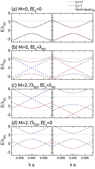
In Fig. 1 we show the energy spectrum for meV and several combinations of and values near both valleys. In the Hamiltonian three types of SOC are included. One is represented by the parameter and introduces a gap in the spectrum as shown in Fig. 1(a). It is diagonal in the spin basis, so both spin components are treated equally. The terms and do mix up the spin states. However, as shown below, the effect of these terms is very small and the spin remains an approximate good quantum number.
The term describes the Rashba SOC due to the field . Note, however, that for a wide range of values this term can be safely neglected since at fields of the order of the critical field , it’s value is approximately .9 ; 4 ; Min2006
A unitary transformation of Eq. allows more insight into the importance of . With the combinations
| (3) | |||||
| (4) |
where and , the new basis transforms Eq. (2) into the form
| (5) |
where and .
The effect of is thus threefold. To first order in it induces a change in the Fermi velocity, , and it couples the spin components by virtue of a finite electric or exchange field. Additionally, it affects the gap to second order in by a diagonal term that is linear in and . However, these effects are very small due to the smallness of . We shall therefore neglect .
II.2 Effective Hamiltonian
The approximations referred to above decouple the two spin states. Because the valleys are independent, we can describe electrons in silicene as particles that have a spin- and valley-dependent gap. In the basis the Hamiltonian becomes
| (6) |
where is the spin quantum number, denotes the valley and equals for and for .
The gap is independent of and given by
| (7) |
Equation (6) corresponds to a 2D Dirac Hamiltonian of particles with mass . Note that in graphene because of the low buckling, both the SOC and the effect of an electric field on the gap are negligible.Min2006 The energy spectrum obtained from Eq. (6) reads
| (8) |
where denotes the electron (hole) states. We show it for all spin and valley components in Fig. 1 for different values of and . In Fig. 1(b) attains its critical value , for which the spin component has a linear massless dispersion, while the one has a large gap near the point. In Fig. 1(c) the field is finite; it displaces both spin components in opposite directions and results in a spectrum that is different for each spin and valley type of electron. In Fig. 1(d) only the field is present and leads to spin polarization but the valleys remain equivalent.
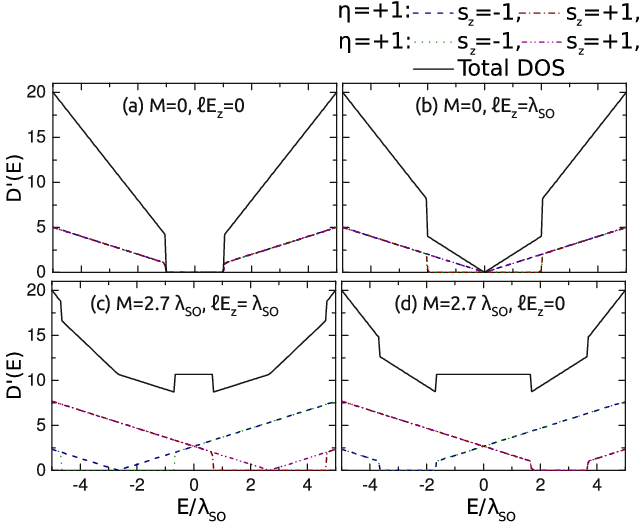
This energy spectrum gives rise to a density of states (DOS) with a structure that depends sensitively on the values of the electric and exchange fields. With the full expression for is Stille2012
| (9) |
We show in Fig. 2 for various values of and . Notice that the DOS depends heavily on the spin and valley index of the electrons. In Fig. 2(c) and (d) for example, the total DOS is constant near zero energy, but it nonetheless consists of different portions of spin-up and spin-down states for each energy.
III Polarization in silicene
To assess electron-electron interactions in the RPA, we first need to determine the polarization:Kotov2008 ; Kotov2008a ; Kotov2012 ; Pyatkovskiy2009
| (10) |
where the summation over corresponds to different valleys and is the Green’s function of the non-interacting particle near the valley. For a finite-mass Dirac Hamiltonian, such as the one shown in Eq. (6), the Green’s function is given byKotov2008 ; Kotov2008a
| (11) | |||||
where we have omitted the identity matrices for the sake of brevity and is the magnitude of . Notice that the dependence of the Green’s function on the spin quantum number is twofold: on the one hand it changes the Fermi level to and on the other it influences the gap given by defined in Eq (7).
We consider only the reduced Hamiltonian (6). For the complete Hamiltonian, we obtain both Green’s functions along the diagonal, so
| (12) |
We can readily calculate the trace in Eq. and write the total polarization as
| (13) |
with the spin- and valley-dependent polarization, obtained in the manner of Ref. Pyatkovskiy2009, , given by
| (14) | |||||
here is an infinitesimal positive quantity, is the Fermi-Dirac distribution with a spin-dependent Fermi level , , and the structure factor
| (15) |
Equation (15) expresses the pseudo spinorial character of electrons in silicene and will prevent two oppositely moving ones from interacting if the gap is zero. This factor is typical for graphene-like 2D systems such as silicene.
Since transitions between different spin and valley states can be neglected, as previously motivated, the resulting polarization is a sum of independent systems. These systems are analogous to gapped graphenePyatkovskiy2009 but in each of them one can change the size of the gap separately by varying the field and the Fermi level can be tuned by changing the field . The spin and valley components are influenced by these fields in different ways.
The contributions to the polarization from Eq. can be written as a sum of three partsWunsch2006 ; Hwang2007a
| (16) |
where stands for interband () or intraband () contributions with Fermi level . The last two terms contribute only for . Note that because the Fermi level is fixed, while the spectrum is displaced or deformed due to the field or , it is possible that this inequality is reversed for one valley spin state while it still holds for the others. In such a case only the vacuum polarization contributes to the polarization of the respective state. Different possible situations are depicted in Fig. 1 in which the Fermi level is shown as a black dotted line. In Figs. 1 (a) and (b) the Fermi level lies in the conduction band of all spin and valley type electrons such that intraband transitions are possible. In Fig. 1 (c), however, this is not the case for spin-up electrons near the valley. The combination of the and fields is such that the Fermi level lies in the band gap of this type of electrons and therefore intraband transitions are excluded in this case. In Fig. 1 (d) the two valleys are equivalent as discussed earlier, but the Fermi level lies in the gap of the spin-up electrons and excludes intraband transitions for them.
Analytical solutions have been found for both the vacuum polarizationKotov2008a ; Pyatkovskiy2009 ; Son2007 and the polarization in graphene with a partly filled conduction band Pyatkovskiy2009 . The polarization for can be written as
| (17) |
where , , , and . Further, is the density of states for one spin component near one Dirac point if and a dimensionless function that acquires different values in different parts of the plane as shown in appendix A.
On the other hand, the vacuum polarization reads
| (18) |
where , . is a dimensionless function defined in appendix A. Combining these results, the total polarization is given by
| (19) |
The complete expression of the dynamical polarization is given in appendix A. The static one can be written as
| (20) |
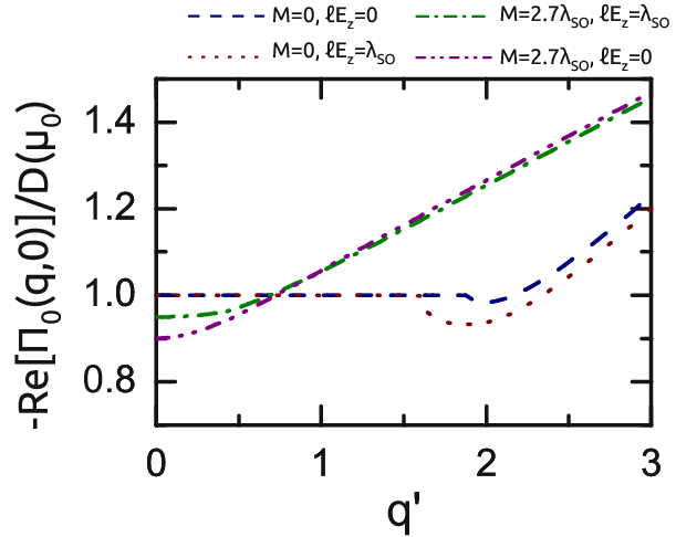
where and ; we used the definition of the Fermi wave vector . For Eq. (20) coincides with the result of Ref. Tabert2014a, and for and with that of Ref. Pyatkovskiy2009, . In Fig. 3 we show the static polarization for various values of the fields and . This figure shows that as long as all spin and valley type electrons contribute, for low , the static polarization equals the DOS at the Fermi level, ), which is the case for the blue dashed and red dotted curves. However, when this is not the case, as for the other two curves, the polarization decreases because in this case, for some spin and valley type electrons only interband contributions are allowed.
Furthermore, one can approximate the polarization at small energies and momenta, asPyatkovskiy2009
| (21) |
which is valid for all values of and .
III.1 Particle-hole excitation spectrum (PHES)
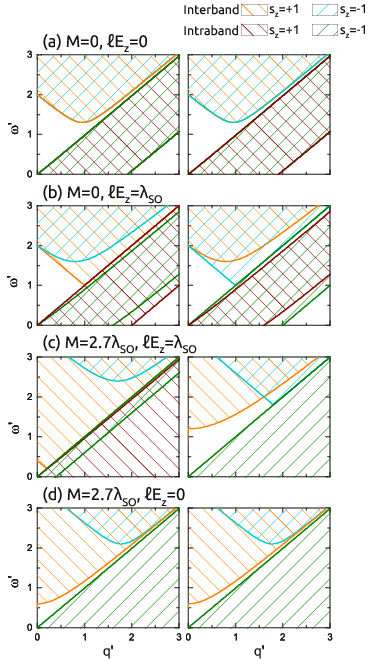
The PHES is the region in the -plane where it is possible for a photon with energy and momentum to excite an electron-hole pair. This ability for pair creation is embodied in the polarization, in the regions where it has a non-zero imaginary part. The PHES can be divided into two disjunct regions where inter- and intraband electron-hole pair formation is possible. These regions are located above and below the line, respectively. Because the fields and change the structure of the bands and the position of the Fermi level, the PHES is also subject to changes in their values. Since the valley and spin of the electrons determine how the fields affect their dispersion and Fermi level, the PHES can be different for electrons with different spin or valley index.
In Fig. 4 we show the PHES of silicene for different values of and for which the energy spectra are shown in Fig. 1. The left column corresponds to electrons in the valley and the right one to the valley.
Figure 4(a) shows that in the absence of the fields both valleys and spins are treated equally and the PHES is the same. When a finite electric field is applied, the gap is changed for each spin and the PHES of each spin near the same Dirac point is different. In the other valley, however, the effect of the electric field has the opposite effect such that the PHES is interchanged between both spin types. Figure 4(b) shows the PHES when the critical electric field is applied. Since for this field one of the two spin states has a gapless dispersion, we obtain the PHES of graphene for the spin-up state near the valley and the spin down-state near the valley. The situation is reversed if points in the opposite direction. For the effect of the electric field on the PHES was investigated in detail in Ref. Tabert2014a,
Changing the exchange field also affects the PHES because the Fermi level of the two spin components is not the same. If the Fermi level of one component is moved inside the bandgap of the corresponding spectrum, the intraband region completely disappears because there are no electrons left in the conduction band. This situation is depicted in Figs. 4(c) and (d) where a finite field is considered. As seen in Fig. 1(c), for which the same fields are considered as Fig. 4(c), the Fermi level of the spin-up electrons is displaced inside the gap near the valley and therefore the intraband PHES is absent in this case. The PHES of different spin and valley type electrons differs strongly, so spin and valley polarization is expected because there are regions in the plane where only one spin and valley type of electrons can create an electron-hole pair.
If the field is absent but the one is finite, the spin symmetry is broken but the valleys remain equivalent. Figure 4(d) shows that the corresponding PHES is strongly spin dependent and spin polarization is possible.
In the region between the intra- and interband PHES, it is not possible to excite a particle-hole pair. Therefore, in this region it is possible to excite stable plasmons. Inside the PHES, the plasmons do have a finite lifetime because they can decay into electron-hole pairs. Notice that the PHES has a spin and valley texture, that is, in some parts of the plane pair formation is allowed for only one spin and one valley component, denoted by , but that there are also regions shared with different components. When pair formation is allowed for only one spin and valley type, it is possible to excite plasmons that contain only one specific spin or valley type of electrons and refer to them as spin- and valley-polarized plasmons.
III.2 Plasmons in the RPA
Using the expression found in Eq. , we can find higher-order contributions, within the RPA, using Goerbig2011 ; GiulianiBook ; Ando1982
| (22) |
where the RPA dielectric function is given by
| (23) |
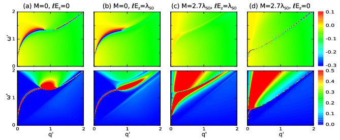
with the 2D Fourier transform of the Coulomb potential with an effective dielectric constant that takes into account the medium surrounding the silicene sample. In this study we consider free-standing silicene and we therefore take , the permittivity of vacuum. In Fig. 5 we plot the real part of the RPA polarization function on the top row.
Using the expressions in Eqs. (17) and (18), we can write the dielectric function as
| (24) |
where with and the fine-structure constant. The value of depends on the material by virtue of the Fermi velocity and on the dielectric constant . For instance, in free-standing silicene we have while for silicene on a substrate, with (e.g. ), decreases to . In this work we consider only free-standing silicene. A new procedure to fabricate it, by intercalating it between two graphene layers, was recently proposed,Berdiyorov2014 ; meh and opens the way for its experimental realization.
The dielectric function determines the amount of absorbed radiation through the relation
| (25) |
In Fig. 5 we show the absorption on the bottom row. The absorption is strong inside the interband PHES because here particle-hole pair formation is possible. There is, however, also a pronounced absorption curve outside the PHES. Here the radiation is not absorbed by pair formation but by plasmons.
Plasmons in the RPA can be found from the zeros of the dielectric function , where is the plasma frequency and the decay rate of the plasmon. Following the standard procedure Wunsch2006 ; Hwang2007a ; Pyatkovskiy2009 we first look for the zeros of the real part of the dielectric function . Later on, we will include the finite lifetime. Note that these plasmons are exact and not damped outside the PHES since the imaginary part of the polarization is zero.
The plasmon dispersion is found by solving the equation numerically. However, for small energies and momenta we can find a near analytical solution upon using Eq. (21). The approximate result is
| (26) |
Note that we obtain again a behaviour. This is typical for plasmons in 2D systems.Krstajic2013a
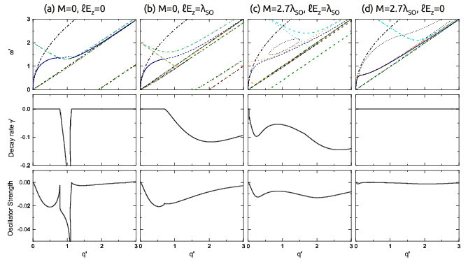
On the first row of Fig. 6 we show the plasmon branches for several configurations of the electric and exchange fields. The solid curves correspond to the plasmons with zero decay rate while the dashed curves are the zeroes of the real part of . The plasmon dispersion given by Eq. (26) is shown by dash-dotted curves.
A more detailed study of the effect of the electric field on plasmons in silicene can be found in Ref. Tabert2014a, ; our results reduce to those of this study for .
III.3 Oscillator strength and decay rate
In this part we calculate the oscillator strength and the decay rate which are related to the robustness of the plasmon. The decay rate determines how fast the plasmon decays after it has been excited. It is given byWunsch2006 ; FetterBook
| (27) |
where is the plasmon frequency for wave vector q. In Fig. 6 on the second row we show the decay rate as a function of the plasmon momentum.
The amount of absorbed radiation by the plasmon is determined by the oscillator strength. In the RPA the imaginary part of the dynamical polarization near the plasmon branch is given byGiulianiBook
| (28) |
and the oscillator strength by
| (29) |
In Fig. 6 we show the oscillator strength for various systems as a function of the wave vector on the third row.
IV Numerical results
The results shown in Figs. 5 and 6 correspond to four systems to which different electric and exchange fields are applied. These four different combinations of and correspond to the values used earlier in Figs. (1)-(4). This allows us to demonstrate the different types of plasmons that can be excited in silicene. In all cases we use meV.
In the first column we show results for a Fermi level but no external fields present. Here both spin types behave the same and we obtain a plasmon branch that is similar to that of gapped graphenePyatkovskiy2009 . Note, however, that because the fine structure constant is twice that of free-standing graphene, it is interrupted by the interband PHES which is accompanied by a strong absorption. Inside the PHES, the decay rate increases very quickly showing the instability of the plasmon at that point. The oscillator strength of the small plasmon branch is larger than that of the second part of the stable branch. The first part is therefore more pronounced than the second one.
In the second column is the critical field, , and the exchange field is zero. This particular example is especially interesting because the spectrum of the electrons is linear and gapless while that of the electrons has a large gap near the valley. The corresponding plasmons have a dispersion that is similar to that of graphene, but which is interrupted by the PHES of the spin-up electrons. The absorption shows that at this point the plasmon can decay into spin-up electron hole pairs near the valley. This is supported by the increase in the decay rate, but note that this rate is much smaller than that for the first case because only one spin type per valley can induce pair formation. The oscillator strength of the plasmon outside the PHES is similar to that of the field-free case, but diminishes inside the PHES. Although the PHES and the plasmons in the two valleys depend on the spin type, they are compensated in the other valley. Therefore, in this case the plasmons are not spin polarized.
In the third column the electric and exchange fields are finite. Because of the combined effect of both fields, the PHES acquires a spin and valley texture. For very small the plasmon branch is stable but it quickly encounters the border of the spin-up PHES where the decay rate increases. The branch continues under the border of the spin-up PHES but the strong absorption signals its presence. The crossing of the border of the spin-down PHES results in a shortening of the lifetime because the plasmons can decay into two different types of electrons, the spin-up type in the valley and the spin down one in the valley. Thus, in this case we obtain spin- and valley-polarized plasmons. Notice an additional feature, the oval dotted curve; this is the remnant of the plasmon branch of spin-down electrons.
The fourth column applies to the case where the electric field is absent but a very large exchange field is applied, . In this situation the dispersions of both spin types are shifted with respect to each other in such a way that the Fermi level lies in the gap of the spin-up electrons while it is situated in the conduction band of the spin-down electrons. For spin-up electrons the intraband PHES therefore vanishes and the interband PHES is shifted to lower energies. Here there is an undamped plasmon branch that follows the border of the interband PHES of the spin-up electrons. Despite its stability, the oscillator strength and absorption show that it is not very pronounced. There exists, however, also a strongly damped branch that lies inside the spin-up interband PHES, shown by the dotted curve, which is the prolonged version of the undamped plasmon and that showing the same dependence of the stable plasmon for low . This branch indicates a spin-down plasmon but one which can decay very quickly into spin-up electron-hole pairs leading to a strong absorption in this region as shown in Fig. 5(d). This plasmon lies outside the PHES and is therefore neither spin- nor valley-polarized. However, the plasmon-like branch inside the spin-up PHES does resemble a spin-polarized system but with a very short lifetime.
V Concluding remarks and outlook
We investigated how electric () and exchange () fields can be used to tune the plasmonic response of the electron gas in silicene. These fields affect the PHES of electrons with opposite spin and valley indices in different ways giving the PHES a spin and valley texture and thus leading to spin- and valley-polarized plasmons. Their lifetime is, however, finite because they can easily decay into electron-hole pairs with different spin or valley indices. Further, the field affects strongly the oscillator strength. The undamped plasmon that remains has a negligible strength and is therefore not expected to show up in experiments. If the Fermi level lies in the gap of a spin in one valley, the intraband region of the corresponding PHES disappears. For zero and finite the spin symmetry is broken and spin polarization is possible.
We found a low-momentum plasmon dispersion that has the typical 2D behaviour. At higher momentum, the plasmon dispersion differs from this dependence. However, a strong field can induce plasmons with finite lifetime of one spin type for which the dispersion follows closely the approximate plasmon branch.
The results reported in this work pertain to free-standing silicene since we used the permittivity of the vacuum. For silicene on a substrate the permittivity will be different and the results will be modified quantitatively. The plasmon branches will be curved downward and the PHES can be avoided yielding plasmons with larger oscillator strength.
We evaluated the plasmon dispersion within the framework of the RPA which is valid for high electron densities. For lower densities further work is necessary to obtain more accurate results for silicene’s plasmonic properties.
The predicted spin-and valley-polarization of plasmons is a consequence of a mechanism similar to that responsible for directional filtering of plasmons in a 2D electron gas.Badalyan2009 In this case the anisotropy of the electron dispersion renders the PHES anisotropic and damps the plasmons in one direction more than in the other.
Recently a lot of experimental progress has been made in the detection of plasmons in 2D materials.Luo2013c To overcome the mismatch of energy and momentum with light in free space, one uses a periodic diffractive grid, cuts the sheet into ribbons or other shapes, and uses an AFM tip to excite the electron liquid or uses a resonant metal antennaAntenna . The appropriate experimental probe though will strongly depend on the setup used to stabilize the silicene crystal. We believe that at the current pace of experimental progress, in the creation of silicene and the probing of plasmons in 2D materials, the results presented in this paper will soon be tested experimentally.
Acknowledgments
This work was supported by the European Science Foundation (ESF) under the EUROCORES Program Euro-GRAPHENE within the project CONGRAN, the Flemish Science Foundation (FWO-Vl) by an aspirant grant to BVD, the Methusalem Foundation of the Flemish Government, and by the Canadian NSERC Grant No. OGP0121756.
Appendix A Analytical formulae
The results for the polarization shown in Eqs. and each depend on a dimensionless function that determines the variation of the polarization in the plane. For the vacuum polarization this function is given in terms of the dimensionless variables , and defined earlier. In the following, we will suppress the prime notation for simplicity and set . ThenPyatkovskiy2009
| (30) |
With , , and , the total polarization for isPyatkovskiy2009
In these expressions
| (31) | |||||
| (32) | |||||
| (33) |
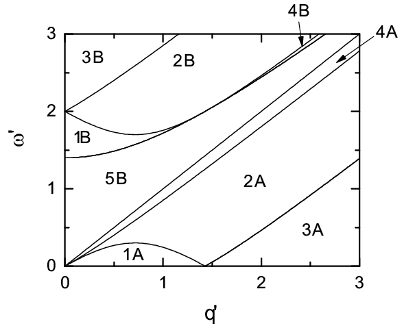
In this solution, we have subdivided the plane in several regions for which the solution is different. We show them in Fig. 7. Setting the borders determining these regions are determined as
Note that the PHES is defined as the region where the imaginary part of the polarization is non zero. This is the case in regions , for the intraband PHES and in regions , , and for the interband PHES of each valley spin state.
References
- (1) A. H. Castro Neto, F. Guinea, N. M. R. Peres, K. S. Novoselov, and A. K. Geim, Rev. Mod. Phys. 81, 109 (2009).
- (2) G. G. Guzmán-Verri and L. C. Lew Yan Voon, Phys. Rev. B 76, 075131 (2007); S. Lebègue and O. Eriksson, ibid. 79, 115409 (2009).
- (3) B. Feng, Z. Ding, S. Meng, Y. Yao, X. He, P. Cheng, L. Chen, and K. Wu, Nano Lett. 12, 3507 (2012).
- (4) P. Vogt, P. De Padova, C. Quaresima, J. Avila, E. Frantzeskakis, M. C. Asensio, A. Resta, B. Ealet, and G. Le Lay, Phys. Rev. Lett. 108, 155501 (2012) .
- (5) A. Fleurence, R. Friedlein, T. Ozaki, H. Kawai, Y. Wang, and Y. Yamada-Takamura, Phys. Rev. Lett. 108, 245501 (2012).
- (6) L.C.L. Yan Voon and G.G. Guzmán-Verri, MRS Bull. 39, 366 (2014).
- (7) A. Kara, H. Enriquez, A. P. Seitsonen, L.C. Lew Yan Voon, S. Vizzini, B. Aufray, and H. Oughaddoub, Surf. Sci. Rep. 67, 1 (2012).
- (8) C. L. Lin, R. Arafune, K. Kawahara, M. Kanno, N. Tsukahara, E. Minamitani, Y. Kim, M. Kawai, N. Takagi, Phys. Rev. Lett. 110, 076801 (2013); Z. X. Guo, S. Furuya, J. Iwata, A. Oshiyama, J. Phys. Soc. Jpn. 82, 063714 (2013); Y. P. Wang, H. P. Cheng, Phys. Rev. B 87, 245430 (2013).
- (9) C.-C Liu , W. Feng, and Y. Yao, Phys. Rev. Lett. 107, 076802 (2011).
- (10) C.-C. Liu, H. Jiang, and Y. Yao, Phys. Rev. B 84, 195430 (2011).
- (11) M. Ezawa, Phys. Rev. Lett. 109, 055502 (2012); New J. Phys. 14, 033003 (2012).
- (12) N. D. Drummond, V. Zólyomi, and V.I. Falko, Phys. Rev. B 85, 075423 (2012).
- (13) Y. Cai, C.-P. Chuu, C. M. Wei, and M. Y. Chou, Phys. Rev. B 88, 245408 (2013).
- (14) H. Liu, J. Gao, and J. Zhao, J. Phys. Chem. C, 117, 10353 (2013).
- (15) M. Neek-Amal, A. Sadeghi, G. R. Berdiyorov, and F. M. Peeters, Appl. Phys. Lett. 103, 261904 (2013).
- (16) M. Tahir, A. Manchon, K. Sabeeh, and U. Schwingenschlögl, Appl. Phys. Lett. 102, 162412 (2013).
- (17) C.J. Tabert and E.J. Nicol, Phys. Rev. B 87, 235426 (2013); I. Ahmed, M. Tahir, and K. Sabeeh, arXiv:1402.6113 (2014).
- (18) C. J. Tabert and E. J. Nicol, Phys. Rev. Lett. 110, 197402 (2013).
- (19) A.N. Grigorenko, M. Polini, and K.S. Novoselov, Nat. Photonics 6, 749 (2012).
- (20) X.-F. Wang and Tapash Chakraborty, Phys. Rev. B 75, 033408 (2007) M. Tahir and K. Sabeeh, J. Phys.: Condens. Matter 20, 425202 (2008); R. Roldan, M. O. Goerbig, and J. -N. Fuchs, Phys. Rev. B 83, 205406 (2011); J. Y. Wu, S. C. Chen, O. Roslyak, G. Gumbs, and M. F. Lin, ACS Nano 5, 1026 (2011); M. Tymchenko, A. Y. Nikitin, and L. M. Moreno, ACS Nano 7, 9780 (2013).
- (21) I. Crassee, M. Orlita, M. Potemski, A. L. Walter, M. Ostler, Th. Seyller, I. Gaponenko, J. Chen, and A. B. Kuzmenko, Nano Lett. 12, 2470 (2012); H. G. Yan, Z. Li, X. Li, W. Zhu, P. Avouris, and F. Xia, Nano Lett. 12, 3766 (2012); J. M. Poumirol, W. Yu, X. Chen, C. Berger, W. A. de Heer, M. L. Smith, T. Ohta, W. Pan, M. O. Goerbig, D. Smirnov, and Z. Jiang. Phys. Rev. Lett. 110, 246803 (2013).
- (22) C.J. Tabert and E.J. Nicol, Phys. Rev. B 89, 195410 (2014);
- (23) H. R. Chang, J. Zhou, H. Zhang, and Y. Yao, Phys. Rev. B 89, 201411 (2014).
- (24) Z. Qiao, S.A. Yang, W. Feng, W.-K. Tse, J. Ding, Y. Yao, J. Wang, and Q. Niu, Phys. Rev. B 82, 161414 (2010).
- (25) H. Haugen, D. Huertas-Hernando, and A. Brataas, Phys. Rev. B 77, 115406 (2008).
- (26) 1 T. Yokoyama, arXiv:1403.1962.
- (27) T. Yokoyama, Phys. Rev. B 87, 241409 (2013).
- (28) M. Tahir and U. Schwingenschlögl, App. Phys. Lett. 101, 132412 (2012).
- (29) H. Min, J.E. Hill, N. A. Sinitsyn, B. R. Sahu, L. Kleinman, and A. H. MacDonald, Phys. Rev. B 74, 165310 (2006).
- (30) L. Stille, C.J. Tabert, and E.J. Nicol, Phys. Rev. B 86, 195405 (2012).
- (31) V. N. Kotov, B. Uchoa, and A. H. Castro Neto, Phys. Rev. B 78, 035119 (2008).
- (32) V. N. Kotov, V. M. Pereira, and B. Uchoa, Phys. Rev. B 78, 075433 (2008).
- (33) V. N. Kotov, B. Uchoa, V. M. Pereira, F. Guinea, and A. H. Castro Neto, Rev. Mod. Phys. 84, 1067 (2012).
- (34) M.O. Goerbig, Rev. Mod. Phys. 83, 1193 (2011).
- (35) S. Das Sarma, S. Adam, E. Hwang, and E. Rossi, Rev. Mod. Phys. 83 407 (2011).
- (36) P. K. Pyatkovskiy, J. Phys.: Condens. Matter 21 025506 (2009).
- (37) B. Wunsch, T. Stauber, F. Sols, and F. Guinea, New J. Phys. 8, 318 (2006).
- (38) E.H. Hwang and S. Das Sarma, Phys. Rev. B 75, 205418 (2007).
- (39) D. T. Son, Phys. Rev. B 75, 235423 (2007).
- (40) P.M. Krstajić, B. Van Duppen, and F.M. Peeters, Phys. Rev. B 88, 195423 (2013).
- (41) G.F. Giuliani, and G. Vignale, 2005, Quantum Theory of the Electron Liquid (Cambridge University, Cambridge)
- (42) T. Ando, A.B. Fowler, and F. Stern, Rev. Mod. Phys. 54, 437 (1982).
- (43) G.R. Berdiyorov, M. Neek-Amal, F.M. Peeters, and A.C.T. van Duin, Phys. Rev. B 89, 024107 (2014).
- (44) A. L. Fetter, J. D. Walecka, 2003, Quantum Theory of Many-particle Systems (Corier Dover Publications)
- (45) S. M. Badalyan, A. Matos-Abiague, G. Vignale, and J. Fabian, Phys. Rev. B 79, 205305 (2009).
- (46) X. Luo, T. Qiu, W. Lu, and Z. Ni, Mater. Sci. Eng. R Reports 74, 351 (2013).
- (47) P. Alonso-Gonzalez, A.Y. Nikitin, F. Golmar, A. Centeno, A. Pesquera, S. Velez, J. Chen, G. Navickaite, F. Koppens, A. Zurutuza, F. Casanova, L.E. Hueso, and R. Hillenbrand, Science 344, 1369 (2014).