Intersubband optical absorption in InSb stepped quantum wells. Effect of spin sublevels crossing.
Abstract
We study linear and non- linear coefficients of the intersubband absorption in InSb-based stepped quantum wells subjected to an in-plane magnetic field. We consider also a transverse electric field to achieve near resonance conditions. Taking into account the two deepest conduction levels and their corresponding Zeeman spin splitting sublevels, we calculate dispersion relations by means of an improved version of Kane model. Besides the known anti-crossing between down and up spin split sublevels, we obtain an extra spin level crossing for some determined parameters. This crossing clearly modifies the absorption spectrum for transitions among the four sublevels considered. We study a low electron density case, when only the first deepest sublevel is occupied, and a high density case with only the highest sublevel empty. We find a similar behavior of the absorption spectrum in both cases.
Keywords: Spin intersubband transitions; Quantum well; Nonlinear optical absorption.
I Introduction
It is well-known that the key of spintronics is the breakdown of the degenerate electronic levels by the spin splitting 1 . This means that spin up and spin down electronic states of any material must necessarily be separated in energy. One way of achieving this splitting is to use two-dimensional electron gas (2DEG) in quantum wells (QWs) . In semiconductor QWs this effect is obtained spontaneously, without external magnetic fields, as long as the confining potential is not symmetrical. Spin splitting will increase due to the contribution of the Zeeman effect when an external in-plane magnetic field is applied 2 ; 3 .
Some semiconductors are particularly suitable materials for spintronics. One of them is the InSb with a large Landé factor (narrow gap), which causes a big magnetic energy and the consequent Zeeman splitting.
Non symmetric heterostructures under in-plane magnetic field show non parabolic dispersion relations. For each electronic level, non parabolic spin split subbands with opposite spin are shifted by the magnetic field in opposite directions of the momentum space. This behavior leads to the presence of anticrossings between subbands for certain momentum values, which are reflected in some peculiarities of the joint density of states and in the excitation photoluminescence spectrum 4 ; 5 ; 6 .
For particular structures with two close electronic levels, high enough magnetic fields can cause a Zeeman splitting of each level bigger than the interlevel energy distance. In this case, together with the momentum-space displacements for different spin sublevels, we have different curvature of quasi parabolas for different electronic levels leading to crossings between the two distinct electronic levels with opposite spins. We should note that, now, we are not talking about anticrossings but crossings, which has been less studied 7 ; 8 ; 9 .
To obtain close enough energy levels, with an intersubband energy distance of the order of the spin splitting, we propose an InSb-based stepped QW.
The standard way to study the optical properties of a material is through electronic transitions that occur after exposing the sample to a perturbation, usually photoexcitation. From a theoretical point of view this means a precise knowledge of the band structure and, hence, the dispersion relations. Several methods were used to calculate the dispersion relations in quantum structures. Among them, the Kane model together with the Transfer Matrix Approximation (TMA), and first order boundary conditions 10 , is particularly suitable for low-symmetry structures because of its versatility. Moreover, this method allows us to add a wide range of perturbations as transverse electric and in-plane magnetic fields. Another effect we can add is abrupt barrier contribution for narrow gap structures.
Optical absorption is one of the most used experimental techniques to study band structures. Absorption spectrum strongly depends on the electronic concentration when heterostructure is selectively doped. Essentially, electronic density is reflected in a variation of the frequency transition between subbands.
The purpose of this work is the study of peculiarities of intersubband optical absorption produced by the crossover of spin sublevels, including electronic concentration effects.
II Theoretical framework
II.1 Eigenstates
In the parabolic approximation, the one-electron Schrödinger equation for stepped QW can be written as 6 ; 11 :
| (1) |
for each 2D momentum , where and , are the eigenfunctions and eigenvalues, respectively. Superscript means barrier or wells (wide and narrow), respectively. The kinetic energy in the in-plane direction, , includes the effective mass . Band diagram for the stepped QW is shown in Fig. 1.

The potential energy is with in the barriers, in the wide well, and in the narrow well. Here is an uniform transverse electric field. and are the band offsets for conduction band between both wells, and between narrow well and barrier, respectively.
For not very strong magnetic fields, we describe the magnetic energy as , where is the Pauli matrix, and is the Zeeman splitting caused by the magnetic field. Here is the effective Landé factor, is the Bohr magneton, and is the in-plane magnetic field. The characteristic spin velocity for each layer is , with the gap energy.
After some heavy algebra 12 , we obtain the fundamental solutions of Eq (1) for spin :
| (2) |
where , with and . In the above equation and are the Airy functions with arguments
| (3) |
with the following auxiliary parameters: the length , and energies , , and . Lastly, , are unknown coefficients that we will obtain by means of the boundary conditions, including abrupt interface parameter 13 , where is the halfwidth of that interface 12 .
The following step is to generate Wronskian-like transfer matrices, which involve contour conditions at interface To obtain electronic levels for each 2D momentum we introduce a modification of the method used before 12 . The total transfer matrix can be written as:
| (4) |
We obtain the exact solution of the Hamiltonian from
| (5) |
The four roots of are the solutions of Eq. (1), , which correspond to the two deepest coupled levels of the stepped QW (), and their respective spin down and spin up sublevels (). For a wide range of values we obtain dispersion relations. We refer to them as quasi-paraboloids because pure paraboloid shape is broken at anticrossing points 4 .
After obtaining coefficients we proceed to calculate wave functions for each energy sublevel () and momentum (Eq. 2). If we denote by the wave function for a particular level , then
| (6) |
where is the Heaviside function. Finally, we normalize wave functions.
Next we will analyze the intersubband absorption coefficient. Because this coefficient is related to the transitions between occupied and empty sublevels, we have to include electron density effects, which determine occupied sublevels. Note that, till now, we have the one-electron solution. Actually, for doped systems hamiltonian should include Hartree and Fock potential terms, and Schrödinger equation has to be solved selfconsistently together with the Poisson equation.
To simplify calculations we assume that, for sheet electron densities of the order of cm-2, electron-electron interaction does not alter one-electron results substantially. Thus, we will neglect Fock term. For the Hartree potential, instead of using the momentum-dependent self-consistency (with the difficulties involved due to dependence), we solve the above one-electron Hamiltonian but taking in mind the noticeable shift in the frequency that Hartree potential produces in the intersubband electronic transitions. This shift is because the photoexcitation electric field produces the superposition of wave functions of the subbands involved in transitions. As a result, the charge density is no longer homogeneously distributed along the direction. The charge redistribution induces a space charge field that overlaps with the laser driving field and affects the interlevel distance. This process is known as depolarization 14 ; 15 ; 16 ; 17 ,. We define the depolarization for the transition as
| (7) |
where , is the permittivity, and is the electron density of the sublevel. Considering the depolarization shift, the renormalized interlevel energy can be expressed as
| (8) |
II.2 Intersubband infrared absorption
To analyze the absorption coefficient we have adapted Ahn and Chuang expressions 18 , obtained with matrix density formalism for parabolic dispersion relations. In our case we deal with non-parabolic dispersion relation and momentum-dependent integrals must be done numerically because the loss of symmetry in the -space. However, calculations are simplified because intersubband transitions between the fundamental and first excited subbands are induced only by light incident parallel to the growth plane 19 . To say, the polarization vector lies in the axis direction. In our case, the linear absorption coefficient for the optical transition between states and , as a function of the incident light frequency and for fixed transverse electric and in-plane magnetic fields, reads
| (9) |
where
| (10) |
are the dipole matrix elements, and
| (11) |
is the well known Fermi-Dirac function for a Fermi energy . The energy broadening of the absorption peaks is where is the intersubband relaxation time. For simplicity, we take an unique value for all transitions. In Eq. (12) is the permeability and is the permittivity of the wells (we take the same values for the two materials), is the light speed in the vacuum, and is the volume of the sample.
The third order nonlinear optical absorption is given by
| (12) |
where is the optical power per unit area. The total absorption coefficient is
| (13) |
Intersubband optical transitions between sublevels with the same spin are called spin conserving transitions, while those that occur between different spin sublevels are often called spin flip transitions.
III Results and discussion
The structure we use in the calculations consists of a stepped QW formed by a Å wide QW of () which includes a Å wide QW of InSb (). The structure is enclosed by barriers. Data for this structure are meV, meV (Fig. 1), , , and , where is the free electron rest mass 20 ; 21 .
For this stepped QW resonance between ground and first excited conduction levels, in absence of magnetic field, is achieved around an electric field meV. In addition to this transverse electric field we apply an in-plane magnetic field to get Zeeman splitting. We find the desired sublevels crossing for T. For higher magnetic fields crossings will occurs at bigger values where first sublevel is empty. For lower magnetic fields there are not spin crossing. Thus, we also use T to compare with the former case.
We consider the structure is selectively doped. To analyze concentration effects we use two density values, cm-2 and cm-2, corresponding to meV and meV, respectively.
III.1 Dispersion relations
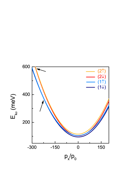
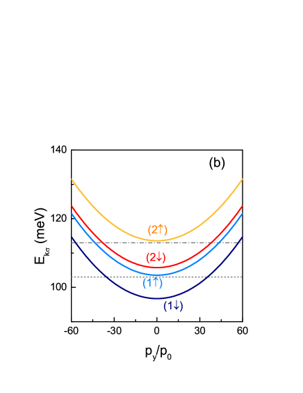
First we look for eigenenergy values by means of Eq. (5). Energy sublevels correspond to the roots of for each value. Looking for the roots over a wide range of momenta we obtain the dispersion relations. Because of the difficulty presented by the quasi-paraboloids to see clearly spin crossings, we draw 2D sections of them, without loss of generality. Fig 2 shows versus for T and . We take as a normalization factor to get dimensionless momentum. Arrows indicate position of anticrossings of the two spin orientations of each energy level. Due to the verticality of the curves in the region where they occur, deformation of the parabolas in the area can not be perceived. Since these anticrossings are not the aim of the present work we focus on the region where crossings occurs.
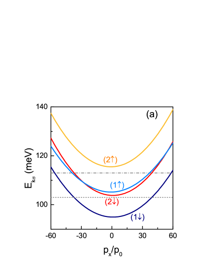
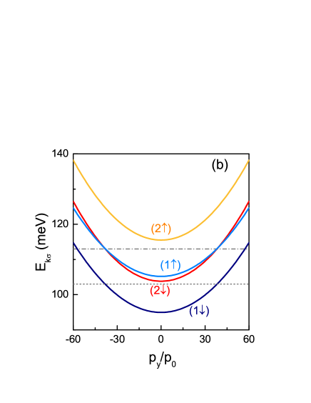
We present crossing region of the former figure in Fig 3(a). Looking at , we can see the parabola is above the one. Since the curvature of the parabolas is greater than that of the parabolas and they shift in opposite directions along axis for different spin values, the crossing of spin sublevels and is obvious for a pair of momentum values. These spin crossings happen around and Beyond these momenta the normal spin order is recovered. For an analogous region, Fig. 3(b) shows versus for . Now, spin crossings are symmetrically placed at .
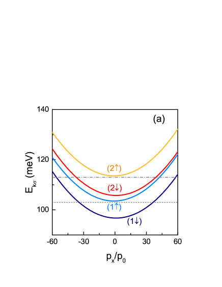
In order to compare with the case where no spin crossings exist, we represent in Fig. 4(a) and 4(b) relation dispersion for T. As can be seen, in this case the parabola is under the one, following the usual behavior. Although these parabolas approximate each other and it would seem that they are crossing, the different curvature of parabolas leads to no crossing at all.
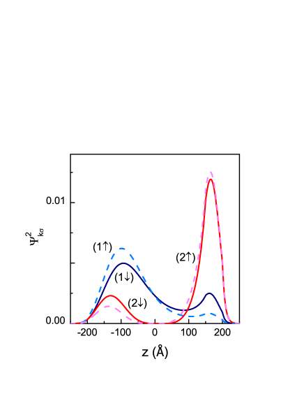
Once obtained dispersion relations we calculate and normalize wave functions As an example Fig. 5 shows the case for T and . Due to the applied electric field kV/cm, just after resonance, the first level is mainly located in the left side of the wide well, whereas the second level basically corresponds to the narrow well. In both cases sublevels are more confined in their corresponding wells, while sublevels are more distributed between the two wells. This behavior will affect the overlap of wave functions and thus, the depolarization shift of transitions frequency.
III.2 Spin intersubband absorption
Next, we calculate dipole matrix elements and, finally, the total absorption coefficient taking into account both linear and non-linear contributions. We take meV, K, and MW/cm2.
First, we consider cm-2 corresponding to meV. In this case only the deepest spin sublevel is occupied, as can be seen in Figs. 3(a-b) and 4(a-b), for T and T, respectively. In these figures, Fermi level is represented by the dotted line. Paraboloids corresponding to the three higher sublevels have energies greater than Fermi energy and are empty. However, the deepest sublevel is below Fermi energy in a certain momentum range. Electrons occupy this region of the bottom of the paraboloid.
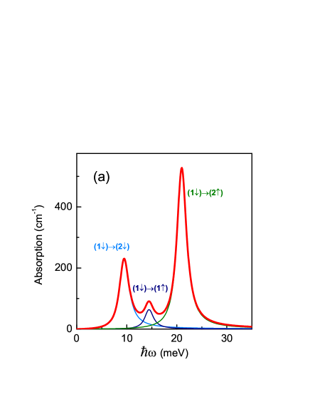
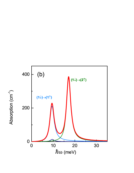
Figs. 6(a-b) show total absorption coefficient for meV and when only the sublevel is occupied. Fig. 6(a) presents the T case, where there is a spin crossing of sublevels. Absorption spectrum shows three peaks corresponding to transitions from this sublevel to the other three empty sublevels , and , respectively, in increasing order of energy. The first is a spin-conserving transition while the other two are spin flip transitions. Fig. 6(b) presents the other case, T, when there is not such a crossing. Now, absorption spectrum displays two dominant peaks, corresponding to transitions from to and . The third peak, for the transition to is too small compared with the others and can not be noticed in the total spectrum.
For cm-2, corresponding to meV, and due to levels proximity, we have three occupied sublevels. This situation is also represented in dispersion relation figures [Figs. 3(a-b) and 4(a-b)], where dash-dotted lines correspond to this Fermi energy value. Unlike the previous case, now only paraboloid corresponding to the highest sublevel has energy greater than Fermi energy and is the only one completely empty. Nevertheless, the other three sublevels cut the Fermi energy for some momentum values leading to the occupation of the bottom of paraboloids with .
Figs. 7(a-b) present absorption coefficient for meV. Now, only sublevel is empty and transitions go from the others sublevels to it. We have also considered the little regions on left and right (in 2D figures but, actually, it is a thin ring in 3D momentum space) of the dispersion relations where sublevels and lay over Fermi energy level, while sublevel is under it. Thus, there are two possible transitions between these sublevels in this -region, from the deepest one to the sublevels and . Nevertheless, results show that the peaks of these transitions are negligible compared with the others and are not visible in the total spectrum. Fig. 7(a) presents the ”spin crossing case”, for T. As in the former situation, we find three peaks corresponding to transitions from spin sublevels , and to sublevel , respectively, in the same increasing order of energy. Fig. 7(b) shows the T case, where there is not spin crossing. In a similar way as found before, we can appreciate only two peaks, because the corresponding to spin-flip transition from sublevel to one is smaller and, due to depolarization shift, almost coincides with the transition from sublevel, resulting in a single peak in the total spectrum. The other peak for the transition from to seems to be similar for the two cases, since spin crossing sublevels are not involved.
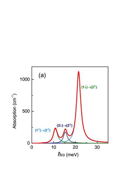
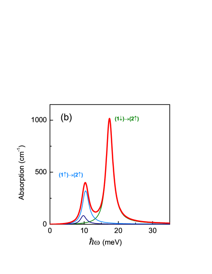
The behavior of the peaks, caused by the depolarization shift, can also be seen for meV in Fig. 6(b). The small peak corresponding to spin-conserving transition to , besides being hardly visible in the total spectrum, almost coincides with the spin-flip transition to .
Considering the four cases under study we can see a general behavior both for transitions from an unique occupied spin sublevel [ , , ], and for transitions up to an unique empty sublevel [, , ], as Figs. 6 and 7 show. The transition between the lower and higher sublevels [ ] gives rise to the dominant absorption peak in every case, specially for higher electronic density. Because of the involved sublevels are not susceptible of crossing, their behavior is similar for both magnetic fields used.
Sublevels and are close together in energy. This would lead to the nearness of the transitions involved: [ , ] and [ , ] (for meV and meV, respectively), and only one peak would be observable. However, when considering the depolarization shift of transitions, absorption peaks separate each other and become distinguishable in the spin crossing case. Depolarization shift depends on wave functions overlapping. It can be proved that overlap corresponding to spin sublevels of the same electronic level [ ] and [ ] is very much greater than that of sublevels of different electronic levels [ ] and [ ]. This fact is reflected in the different energy shifts of the corresponding absorption peaks.
When spin crossing exists and for meV [Fig. 6(a)], absorption peaks follow the order in energy [ ], [ ]. By considering shift caused by depolarization, displacement of second transition [ ] is much greater than that of the first one and both peaks separate each other and become clearly visible in the total spectrum. A similar situation occurs for meV [Fig. 7(a)], where the order of transitions is [ ], [ ]. Again, peak corresponding to second transition shifts more than that of the other and both are discernible.
When there is not spin crossing the position of the transitions is inverted [Figs. 6(b) and 7(b)]. In this case, the larger displacement of the first peak makes it almost coincident with the second one, showing an unique peak for both transitions. Results are in agreement with available experimental data for the case where there is not spin sublevel crossing 22 and other theoretical works for stepped quantum wells 23 .
IV Conclusions
In this work we calculate linear and non-linear intersubband optical absorption coefficients in InSb-based stepped quantum wells, including electron density effects through the displacements of transitions caused by depolarization. We use a modified version of the Kane model together with the TMA, which includes transverse electric field, in-plane magnetic field and abrupt interfaces contribution to obtain the dispersion relations. Considering Zeeman splitting of the electronic levels, we find spin sublevel crossing or intersection of quasi-paraboloids for certain values of the magnetic field. The existence of spin sublevel crossing essentially modifies absorption spectrum: it changes the energy order of the electron transitions which, together with the depolarization shift, provides an additional peak in the structure of the absorption spectrum when compared with the standard non crossing situation.
A similar theoretical analysis may be developed for the study of optical properties in other structures under magnetic field. We hope that present results will stimulate experimental efforts towards the study of spin crossing peculiarities in nanostructures.
References
- (1) J. M. Kikkawa and D. D. Awschalom, ”Resonant Spin Amplification in n-Type GaAs”, Phys. Rev. Lett. 80(19), 4313-4316 (1998).
- (2) J. Xia, W. Ge, and K. Chang, Semiconductor Spintronics (World Scientific, 2012).
- (3) R. Winkler, Spin-Orbit Coupling Effects in Two-Dimensional Electron and Hole Systems (Springer-Verlag, Berlin, 2003).
- (4) A. Hernández-Cabrera, P. Aceituno, and F. T. Vasko, ”Level anticrossing effect on electron properties of coupled quantum wells under an in-plane magnetic field”, Phys. Rev. B 60(8), 5698-5704 (1999).
- (5) D. Huang and S. K. Lyo, ”Photoluminescence spectra of n-doped double quantum wells in a parallel magnetic field”, Phys. Rev. B 59, 7600(1999). S. K. Lyo, ”Transport and level anticrossing in strongly coupled double quantum wells with in-plane magnetic fields”, Phys. Rev. B 50(7), 4965-4968 (1994)
- (6) A. Hernández-Cabrera, P. Aceituno, and F. T. Vasko, ”Electron energy spectrum and density of states for nonsymmetric semiconductor heterostructures in an in-plane magnetic field”, Phys. Rev. B 74(3), 035330 (2006).
- (7) A. C. Graham, K. J. Thomas, M. Pepper, N. R. Cooper, M. Y. Simmons, and D. A. Ritchie, ”Interaction Effects at Crossings of Spin-Polarized One-Dimensional Subbands”, Phys. Rev. Lett. 91(13), 136404 (2003).
- (8) K. F. Berggren, P. Jaksch, and I. Yakimenko, ”Effects of electron interactions at crossings of Zeeman-split subbands in quantum wires”, Phys. Rev. B 71(11), 115303 (2005).
- (9) Y. V. Pershin, J. A. Nesteroff, and V. Privman, ”Effect of spin-orbit interaction and in-plane magnetic field on the conductance of a quasi-one-dimensional system”, Phys. Rev. B 69(12), 121306(R) (2004).
- (10) F. T. Vasko, ”Spin splitting in the spectrum of two-dimensional electrons due to the surface potential”, JETP Lett. 30(9), 541-544 (1979).
- (11) A. Hernández-Cabrera, P. Aceituno, and F. T. Vasko, ”Quantum wells under an in-plane magnetic field: Effect of the composition parameters on excited electron energy splitting”, Journal of Luminescence 128(5-6), 862-864 (2008).
- (12) A. Hernández-Cabrera and P. Aceituno, ”Abrupt barrier contribution to electron spin splitting in asymmetric coupled double quantum wells”, Indian J. Phys. DOI 10.1007/s12648-014-0515-5 (2014).
- (13) F. T. Vasko and A. V. Kuznetsov, Electronic States and Optical Transitions in Semiconductor Heterostructures (Springer, New York,1999).
- (14) M. Zaluzny, ”Influence of the depolarization effect on the nonlinear intersubband absorption spectra of quantum wells”, Phys. Rev. B 47(7), 3995-3998 (1993).
- (15) R. J. Warburton, C. Gauer, A. Wixforth, J. P. Kotthaus, B. Brar, and H. Kroemer, ”Intersubband resonances in InAs/AlSb quantum wells: Selection rules, matrix elements, and the depolarization field”, Phys. Rev. B 53(12), 7903-7910 (1996)
- (16) A. A. Batista, P. I. Tamborenea, B. Birnir, M. S. Sherwin, and D. S. Citrin, ”Nonlinear dynamics in far-infrared driven quantum-well intersubband transitions” Phys. Rev. B 66(19), 195325 (2002).
- (17) A. Hernández-Cabrera and P. Aceituno, ”Calculation of intersubband absorption in doped graded quantum wells under intense terahertz irradiation”, Phys. Rev. B 78(3), 035302 (2008).
- (18) D. Ahn and S. L. Chuang, ”Calculation of linear and nonlinear intersubband optical absorptions in a quantum well model with an applied electric field”, IEEE J. Quantum Electron. 23(12), 2196-2204 (1987).
- (19) M. Virgilio and G. Grosso, ”Optical transitions between valley split subbands in biased Si quantum wells”, Phys. Rev. B 75(23), 235428 (2007).
- (20) D. W. Palmer, ”The Semiconductors Information”, http://www.semiconductors.co.uk/ propiiiv5653.htm. Ioffe Physico-Technical Institute, ”New Semiconductor Materials. Characteristics and Properties”, http://www.ioffe.rssi.ru/SVA/NSM/Semicond/InSb/.
- (21) M. Edirisooriya, T. D. Mishima, C. K. Gaspe, K. Bottoms, R. J. Hauenstein, M. B. Santos, ”InSb quantum-well structures for electronic device applications”, J Crystal Growth 311(7), 1972-1975 (2009).
- (22) M. B. Santos, S. D. Lowe, T. D. Mishima, R. E. Doezema, L. C. Tung, and Y.-J. Wang, ”Intersubband Absorption by Electrons in InSb Quantum Wells with an In-Plane Magnetic Field”, AIP Conf. Proc. 1399, 133 (2011).
- (23) F T Vasko and G Y Kis, ”The effect of a longitudinal magnetic field on electronic intersubband transitions in asymmetric heterostructures”, Semiconductors 31(9), 961-965 (1997).