Strongly anisotropic ballistic magnetoresistance in compact three-dimensional semiconducting nanoarchitectures
Abstract
We establish theoretically that in non-magnetic semiconducting bilayer or multilayer thin film systems rolled-up into compact quasi-one-dimensional nanoarchitectures, the ballistic magnetoresistance is very anisotropic: conductances depend strongly on the direction of an externally applied magnetic field. This phenomenon originates from the curved open geometry of rolled-up nanotubes, which leads to a tunability of the number of one-dimensional magnetic subbands crossing the Fermi energy. The experimental significance of this phenomenon is illustrated by a sizable anisotropy that scales with the inverse of the winding number, and persists up to a critical temperature that can be strongly enhanced by increasing the strength of the external magnetic field or the characteristic radius of curvature, and can reach room temperature.
pacs:
75.47.-m, 73.20.At, 75.75.-c, 85.75.-dIn 1857 Thomson discovered that the resistivity of bulk ferromagnetic metals depends on the relative angle between the electric current and the magnetization direction Thomson . The prediction of this anisotropic magnetoresistance (AMR), caused by an anisotropy in the electron scattering due to spin-orbit interaction, was experimentally verified more than a century later in iron, cobalt, and nickel alloys. Since then, the interest in this phenomenon has received a boost thanks to the development of AMR sensors for magnetic recording amr-fe ; amr-book .
It was recently proposed that this phenomenon might also occur in ferromagnetic Fe and Ni nanowires bal-ma . Contrary to macroscopic samples, in miniaturized objects with characteristic dimensions less than the electronic mean free path, electronic transport is ballistic rather than diffusive, and electron scattering does not contribute to the conductance. The ballistic conductance of a quasi one-dimensional (1D) magnetic nanostructure with a slowly varying constriction of width of the order of the Fermi wavelength is indeed simply given by where is the number of open conducting channels qnc-q . Due to the strong spin-orbit coupling in these nanostructures, the number of transverse modes at the Fermi energy changes with the magnetization direction and leads ultimately to a ballistic anisotropic magnetoresistance (BAMR).
In this Letter, we show that a strong BAMR occurs in the electronic quantum transport of compact quasi-1D tubular nanostructures obtained by the self-rolling of strained thin films firstn , when subject to an externally applied magnetic field. Contrary to the nanostructures of magnetic materials mentioned above, the BAMR in these nanoarchitectures is entirely due to the open curved geometry of the rolled-up tubes, which breaks the rotational symmetry of the three-dimensional (3D) embedding space. As a result, rolled-up tubes of conventional non-magnetic semiconducting materials display a sizable BAMR, which scales with the inverse of the number of windings of the tubes, and persists up to a temperature that can be tuned to be as large as room temperature by tailoring either the strength of the magnetic field or the radius of curvature.
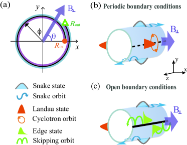
Our starting point is a curved two-dimensional electron gas (2DEG) in a GaAs heterojunction (effective mass ), as obtained by selective underetching of pseudomorphically strained bilayer [c.f. Fig. 1(a)] or multilayer semiconducting thin films Mendach-apl ; Mendach-chapter ; qhe1 ; gmr ; qhe2 . We consider the length of the tube along its axis to be smaller than the characteristic mean free path of the high-mobility curved 2DEG (m in (Al,Ga)As heterojunctions qhe1 ). We also assume the inner radius of curvature, , and the outer radius of curvature, where is the winding number and the total thickness of the layer stack in which the 2DEG is embedded, to be nm, and thus comparable to the large Fermi wavelength nm of the low-density electron gas. Such a compact 3D nanoarchitecture can also be viewed as a curved quantum point contact (QPC) qtransport ; qpcprl with circular cross section and width corresponding to the diameter of the nanotube. In this regime, quantum-size effects appear that lead to ballistic conductance quantization both at zero-field and in the presence of a magnetic field qpcprl . In the latter case the nature of the quantum states, and thus the ballistic conductance itself, strongly depends on whether one considers open or periodic boundary conditions.

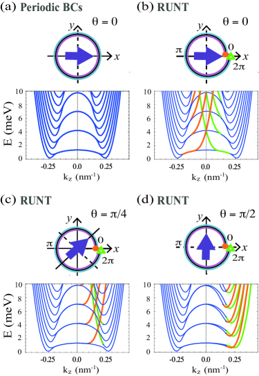
To show this, we first neglect the difference between the inner and the outer radius of the nanotube (), and thus consider a cylindrical 2DEG with periodic boundary conditions in an external magnetic field nt1 ; gaasnt1 , for which the radius of curvature is much larger than the Landau magnetic length . Since the radius of curvature is in the hundreds of nanometers scale, this regime can be reached already if magnetic fields on the scale of one Tesla are externally applied. This also implies that one can neglect the Zeeman splitting removing the spin degeneracy and take only into account the orbital effect of the magnetic field. The large separation between the Landau magnetic length and the radius of curvature allows for the formation of cyclotron orbits centered at the two positions where the tangential plane of the nanostructure is orthogonal to the magnetic field direction [see Fig. 1(b)]. The appearance of cyclotron orbits is reflected, in turn, in the formation of doubly-degenerate quasi-1D Landau-like states. This is demonstrated in Fig. 2(a), where we show the energy spectrum of a 2DEG confined to a cylindrical surface costa ; strain under the influence of a transversal magnetic field of strength T prlsch ; aq3 [see Supplemental Material supple ]. At large values of the momentum along the translationally invariant tube axis direction, the flat quasi-1D Landau-like subbands, however, start to acquire a characteristic parabolic dispersion [c.f. Fig. 2(a)]. One can identify these dispersive states as snake states mul92 centered, due to Lorentz force, at the two points where the tangential plane of the nanostructure is parallel to the magnetic field direction [c.f. Fig. 1(b)]. As we show in the Supplemental Material, the appearance of snake electron trajectories results from the fact that in the immediate vicinity of the orbit centers the spatially inhomogeneous normal component of the externally applied magnetic field switches sign.
Next, we explicitly take into account the difference between the inner and outer radius of curvature, and, following Ref. runt, , consider the 2DEG confined to a cylindrical surface whose cross section is approximated by an Archimedean spiral with polar equation . We assume periodic boundary conditions along the tube axis , and open boundary conditions with along the azimuthal direction. The qualitative change in the nature of the quantum states for the open geometry is shown in Fig. 1(b) where we sketch the different quantum states appearing in a single wound () rolled-up nanotube (RUNT), subject to a magnetic field whose direction with respect to the edge axis [c.f. Fig. 1(a)] is set to zero. We emphasize that generally the winding number will take a non-integer value due to the unavoidable presence of overlapping fringes as found in experiments firstn and computer simulations zan07 . This, however, does not qualitatively change the main features of the magnetic spectra, which are entirely set by the presence, and not the precise location, of the open boundaries.
The presence of the boundaries does not influence the formation of the snake states discussed above. However, due to the hard walls, one of the two cyclotron orbits encountered in the closed geometry fractionalizes into two skipping orbits for which a clear dispersion along is expected. Fig. 2(b) shows the ensuing energy spectrum with nm, nm and a magnetic field strength, as before, of 1.65 T [see Supplemental Material]. One can identify a single non-degenerate quasi-1D Landau-like state now coexisting for with two dispersive edge states localized at the inner and outer radius of the RUNT, which distinctly differentiate the magnetic spectra of rolled-up tubular nanostructures with respect to seamless tubes as carbon nanotubes.

Having established the qualitative difference between the magnetic spectra with periodic and open boundary conditions, we now discuss the interplay between the location of the hard-wall boundaries and the direction of the externally applied magnetic field. Since, as mentioned above, the open curved geometry of a spiral RUNT breaks the rotational symmetry of the embedding 3D space, the features of the magnetic spectra are drastically altered as the direction of the magnetic field changes. This is immediately manifested in Fig. 2 where we show the evolution of the magnetic spectrum of Fig. 2(b) by applying two consecutive 45∘ tilts of the magnetic field while keeping its strength constant. As shown in Fig. 2(c) the first 45∘ rotation of the magnetic field direction restores a quasi-1D Landau state doublet for due to the insensitiveness of the small radii cyclotron orbits centered at to the hard-walls. The same holds true for the snake states at large values of whose orbits are centered at . On top of this, we find the two edge states with skipping orbits at the inner and outer radius of the nanotube to appear for intermediate values of momentum [c.f. the green and orange lines in Fig. 2(c)]. Considering instead the magnetic field direction perpendicular to the edge axis leads to the magnetic spectrum shown in Fig. 2(d). It strongly resembles the spectrum for the periodic boundary conditions of Fig. 2(a) with the following caveat: due to the hard-walls the snake states at large momenta are substituted by edge states. This, however, does not change qualitatively the magnetic spectrum apart from an asymmetry in the dispersion around due to the different nature of the magnetic states, i.e. snake orbits for and skipping orbits for .

The aforementioned features of the magnetic spectra persist up to a critical energy scale given by the characteristic Landau level energy splitting , with the cyclotron frequency, renormalized by a geometrically tunable factor [see Fig. S2 in Supplemental Material]. This results from the following classical trajectories analysis: the existence of quasi-1D Landau levels is preserved as long as the radius of the cyclotron orbits – with the Fermi momentum – does not exceed the curvature radius. In the opposite regime, indeed, traversing trajectories qtransport appear, and, independent of the magnetic field direction, edge and snake states coexist with magnetoelectric subbands. For a 2DEG in GaAs heterojunctions, we find the threshold between the two regimes for our chosen parameter set to be meV – an energy larger than at room temperature.
With the magnetic spectra for different magnetic field directions in our hands, we have then determined the ballistic conductance of our single-wound nanotube neglecting intersubband scattering processes qpc-book ; buttprl ; static-C ; Imry-book ; ibm-qpc . Within this approximation, the Landauer formula for the two-terminal conductance including the thermal smearing of the Fermi-Dirac distribution becomes japan-qc ; bag-lg
| (1) |
where indicates the Fermi-Dirac distribution, is the Fermi energy while is the conductance at zero temperature proportional to the number of occupied magnetoelectric subbands. Fig. 3(a) shows the behavior of the low-temperature magnetoconductance as a function of the inverse of the Fermi wavelength of the 2DEG . Here is the electron density given by
| (2) |
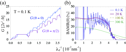
where the index runs over the occupied one-dimensional subbands, is the total arclength of the nanotube section and the factor of accounts for spin degeneracy. Independent of the direction of the externally applied magnetic field, the low-temperature magnetoconductance shows as a step-like increase, which is a direct consequence of the effective one-dimensionality of the curved nanoarchitecture. However, the different features of the magnetic spectra reported in Fig. 2 lead to a substantial BAMR whose magnitude we define bal-ma as
measured from the reference direction perpendicular to the edge axis where the ballistic conductance takes its minimum value. In Fig. 3(b) we illustrate the relevance of the BAMR effect by showing that the magnitude at extends over a wide range of , and persists down to the critical Fermi wavelength ( nm for our set of parameters) where the cyclotron orbit’s radius balances the radius of curvature.

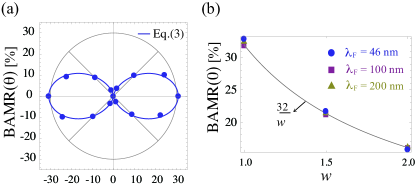
The conductance steps disappear at temperatures , i.e. when the width of the thermal smearing is larger than the subband splitting at the Fermi level. Remarkably, this thermal broadening does not endanger the occurrence of the BAMR. The onset of the anisotropy in the magnetoconductance is indeed regulated by the appearance of quasi-1D Landau states with cyclotron orbits, one of which, by tilting the magnetic field, fractionalizes into skipping orbits contributing to the conductance. As mentioned above, this occurs at the energy scale , which is much larger than the subband splitting meV. In Fig. 3(b) we prove indeed that a sizable BAMR survives at room temperature. Even more, as the effect of the thermal broadening increases, we find that the angular dependence of the BAMR [see Fig. 4(a)] can be accurately described by assuming the functional form of the resistivity for the classical anisotropic magnetoresistance effect bal-ma
| (3) |
On top of this, we find the BAMR effect to be robust and independent of geometric details. We have indeed generalized our calculations to RUNTs with winding numbers [see Supplemental Material] and found that the BAMR magnitude [c.f. Fig. 4(b)], as it can be intuitively understood by considering that the number of snake and Landau states scales as while the number of edge states is independent of it.
To sum up, we have predicted the existence of a ballistic anisotropic magnetoresistance – a change in the ballistic conductance with the direction of an externally applied magnetic field – in compact rolled-up tubular nanostructures of conventional non-magnetic semiconducting materials first ; runt-c ; review-exp ; si ; si-sio . The occurrence of this phenomenon is entirely due to the open curved geometry of these nanoarchitectures and is thus independent of geometric details of the nanostructures. A classical electron trajectories analysis shows that a sizable BAMR occurs whenever the Fermi wavelength of the 2DEG and persists even in the classical regime up to a critical temperature . As a result, a strong anisotropy in the magnetoconductance can be expected at room temperature and weak external magnetic fields in present day curved nanostructures manufactured with the rolled-up nanotechnology firstn ; fet where radii of curvatures in the hundreds of nanometer range can be achieved.
Acknowledgements – We acknowledge the financial support of the Future and Emerging Technologies (FET) programme within the Seventh Framework Programme for Research of the European Commission, under FET-Open grant number: 618083 (CNTQC). C.H.C. acknowledge support from the Ministry of Science and Technology of Taiwan (No: 102-2917-I-564-054).
References
- (1) W. Thomson, Proc. Royal Soc. London 8, 546 (1857).
- (2) T. R. McGuire and R. I. Potter, IEEE Trans. Magn. 11, 1018 (1975).
- (3) R. C. O’Handley, Modern Magnetic Materials: Principles and Applications (Wiley, New York, 2000), p. 573.
- (4) J. Velev, R. F. Sabirianov, S. S. Jaswal, and E. Y. Tsymbal, Phys. Rev. Lett. 94, 127203 (2005).
- (5) R. Landauer, IBM J. Res. Dev. 32, 306 (1988).
- (6) O. G. Schmidt and K. Eberl, Nature (London) 410, 168 (2001).
- (7) S. Mendach, O. Schumacher, H. Welsch, C. Heyn, W. Hansen, and M. Holz, Applied Physics Letters 88, 212113 (2006).
- (8) K. Peters, S. Mendach, and W. Hansen, in Quantum Materials, Lateral Semiconductor Nanostructures, Hybrid Systems and Nanocrystals, NanoScience and Technology, edited by D. Heitmann (Springer Berlin Heidelberg, 2010), pp. 25–49.
- (9) K.-J. Friedland, R. Hey, H. Kostial, A. Riedel, and K. H. Ploog, Phys. Rev. B 75, 045347 (2007).
- (10) A. B. Vorob’ev, K.-J. Friedland, H. Kostial, R. Hey, U. Jahn, E. Wiebicke, J. S. Yukecheva, and V. Y. Prinz, Phys. Rev. B 75, 205309 (2007).
- (11) K.-J. Friedland, A. Siddiki, R. Hey, H. Kostial, A. Riedel, and D. K. Maude, Phys. Rev. B 79, 125320 (2009).
- (12) C. W. J. Beenakker and H. van Houten, Solid State Physics 44, 1 (1991).
- (13) B. J. van Wees, H. van Houten, C. W. J. Beenakker, J. G. Williamson, L. P. Kouwenhoven, D. van der Marel, and C. T. Foxon, Phys. Rev. Lett. 60, 848 (1988).
- (14) G. Ferrari, A. Bertoni, G. Goldoni, and E. Molinari, Phys. Rev. B 78, 115326 (2008).
- (15) G. Ferrari, G. Goldoni, A. Bertoni, G. Cuoghi, and E. Molinari, Nano Lett. 9, 1631 (2009).
- (16) R. C. T. da Costa, Phys. Rev. A 23, 1982 (1981).
- (17) C. Ortix, S. Kiravittaya, O. G. Schmidt, and J. van den Brink, Phys. Rev. B 84, 045438 (2011).
- (18) G. Ferrari and G. Cuoghi, Phys. Rev. Lett. 100, 230403 (2008).
- (19) C. Ortix and J. van den Brink, Phys. Rev. B 83, 113406 (2011).
- (20) See Supplemental Material [url], which includes Refs. [21-22].
- (21) B. Lassagne, J.-P. Cleuziou, S. Nanot, W. Escoffier, R. Avriller, S. Roche, L. Forró, B. Raquet, and J.-M. Broto, Phys. Rev. Lett. 98, 176802 (2007).
- (22) U. C. Coskun, T.-C. Wei, S. Vishveshwara, P. M. Goldbart, and A. Bezryadin, Science 304, 1132 (2004).
- (23) J. E. Müller, Phys. Rev. Lett. 68, 385 (1992).
- (24) C. Ortix and J. van den Brink, Phys. Rev. B 81, 165419 (2010).
- (25) J. Zang, M. Huang, and F. Liu, Phys. Rev. Lett. 98, 146102 (2007).
- (26) H. van Houten, C. W. J. Beenakker, and B. J. van Wees, in Semiconductors and Semimetals, edited by M. A. Reed (Academic Press, New York, 1992), Vol. 35.
- (27) M. Büttiker, Phys. Rev. Lett. 57, 1761 (1986).
- (28) E. N. Economou and C. M. Soukoulis, Phys. Rev. Lett. 46, 618 (1981).
- (29) Y. Imry, in Directions in Condensed Matter Physics, edited by G. Grinstein and G. Mazenko (World Scientific, Singapore, 1986), Vol. 1.
- (30) A. D. Stone and A. Szafer, IBM J. Res. Dev. 32, 384 (1988).
- (31) Y. Isawa, J. Phys. Soc. Japan 57, 3457 (1988).
- (32) P. F. Bagwell and T. P. Orlando, Phys. Rev. B 40, 1456 (1989).
- (33) V. Prinz, V. Seleznev, A. Gutakovsky, A. Chehovskiy, V. Preobrazhenskii, M. Putyato, and T. Gavrilova, Physica E 6, 828 (2000).
- (34) S. Mendach, O. Schumacher, C. Heyn, S. Schnüll, H. Welsch, and W. Hansen, Physica E 23, 274 (2004).
- (35) X. Li, J. Phys. D: Appl. Phys. 41, 193001 (2008).
- (36) R. Songmuang, C. Deneke, and O. G. Schmidt, Appl. Phys. Lett. 89, 223109 (2006).
- (37) R. Songmuang, A. Rastelli, S. Mendach, and O. G. Schmidt, Appl. Phys. Lett. 90, 091905 (2007).
- (38) D. Grimm, C. C. Bof Bufon, C. Deneke, P. Atkinson, D. J. Thurmer, F. Sch ffel, S. Gorantla, A. Bachmatiuk, and O. G. Schmidt, Nano Lett. 13, 213 (2013).