Conductance footprints of impurity scattering in graphene nanoribbons
Abstract
We report a detailed analytic investigation of the interplay between size quantization and local scattering centers in armchair graphene nanoribbons, as seen in the conductance. The scattering property of a local scattering center is dependent on if it is located on one sublattice (A-site impurity) or both (impurity situated at neighboring carbon atoms, A-B-site impurity). The A-site impurity scatters in a similar fashion as a localized impurity in a one-dimensional channel made from a two-dimensional electron gas. On the other hand, the A-B-site impurity includes multiple scattering involving A- to B-sublattice scattering, which knows about the chirality of the Dirac electrons and heavily influence the conductance. For A-site impurities, an intricate interplay between evanescent waves at the impurity and the propagating modes contributing to the conductance, leads to scattering resonances that generate either dips in the conductance or render the impurity completely transparent. The latter occurs at subband bottom energies , where the wave vector of mode turns to zero. The conductance ( the conductance quantum) of defect free graphene therefore remains at these energies after adding one A-site impurity. This is analagous to the case of a scattering center in a quantum channel made from a two-dimensional electron gas. The conductance dips occur at energies from the conductance steps and their location depend directly on the impurity strength . In particular, for repulsive impurities () the dips occur for hole-doping, while for attractive impurities () for electron doping. For an A-B-site impurity, the A- to B-sublattice scattering interferes with the transmission resonance at the energies of the subband bottoms and the impurity is never transparent and the conductance steps of defect free graphene ribbons are always lost. We derive a generalized Fisher-Lee formula for graphene leads that holds for arbitrary scattering region and arbitrary number of leads.
pacs:
73.23.-b, 73.22.PrI Introduction
A great challenge in graphene technology is the fabrication of nanostructures free from disorder and impuritiesCastroNetoReview ; PeresReview ; NovoselovRoadmap (such as defects, adatoms, vacancies and edge disturbances). With a lot of research put into the field, the graphene community has gotten closer to the goal of producing such atomically clean structures. Fabrication methods include both top-down approaches (such as scanning probe methodsConnollyReview ; DeshpandeReview , nano-litography,HanPRL2007 directional etching using nanoparticlesCamposNanoLett2009 or rearranging atoms using TEMGiritScience2009 ) and bottom-up approches (such as chemical synthesisCaiNature2010 or the unzipping of carbon nanotubesLiScience2008 ). These have all proven to be useful, but so far not perfect.BanhartReview
Experiments on one type of such nanostructures, graphene nanoribbons (GNRs), reveal that they are not ideal, and much work, theoretical and experimental, has been aimed at explaining how the transport properties of GNRs are effected by the disorder and impurities normally present in the ribbons. Typical attributes of non-ideal ribbons, such as absence of conductance quantization and the development of a conductance gap, has thus been given much attention, see the reviews in Ref. RazaCollection, ; KatsnelsonBook, ; RocheBook, .
In this paper, we make an analytical study of graphene nanoribbons with perfect armchair edges (ANGRs). In particular, we examine in detail how the interplay between size-quantization and localized scattering centers changes the transmission properties of the ribbons. We base our analytical work on a Fisher-Lee type relationFisherLee between the single-electron propagators and the current-transmission amplitudes. As seen in many numerical studies,RazaCollection ; KatsnelsonBook ; RocheBook we find that the presence of a localized scattering center causes characteristic dips in the conductance through the system when the Fermi energy approaches the bottom of a higher energy subband. The origin of this behavior is the build-up of evanescent waves and quasi-bound states around the scatterer that causes resonant backscattering of the propagating waves. We also show that, for A-site impurities (see below), the backscattering vanishes completely and the transmission recovers its original value when the Fermi energy exactly touches the higher energy subband. This is analagous to what has been found in previous works on one-dimensional channels made from two-dimensional electron gases.Bagwell1 ; Bagwell2 For A-B-site impurities, the resonances are heavily influenced by the A- to B-site scattering events. This is unique to graphene and we will highlight its consequences.
II Impurity scattering including quantum confinement
The problem of scattering against a localized defect in an otherwize perfect 2D sheet of graphene has been studied in several works, see for instance the review in Ref. WehlingReview, In particular, it has been shown that impurity resonances (quasibound) states can be formed. If the potential strength of the localized impurity is very large, the resonance can approach the Dirac point according to the approximate formula , where is a high-energy cut-off beyond which the Dirac approximation is invalid ( in graphene, where the nearest neighbor hopping amplitude). In the presence of a random distribution of such impurities, an impurity band may form which at low temperatures and energies can dominate transport properties.GusyninPRL2005 ; PeresPRB2006 ; LofwanderPRB2007
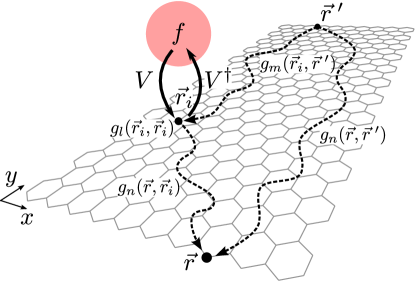
For the case of quantum confinement, impurity scattering will be very different.BergvallPRB2013 Consider an AGNR as illustrated in Fig. 1 with a scattering region, here simply a localized impurity at , attached to perfect leads near and . The leads extend far to reservoirs in the spirit of Landauer and Büttiker.LandauerButtiker The zero temperature Landauer formula reads
| (1) |
where is the conductance quantum and the transmission from mode in the source electrode to in the drain. The sum is here taken over all propagating modes, i.e., all modes where the momenta are real valued. Note, however, that evanescent modes are included as intermediate scattering channels in the calculation of the transmission function, i.e. evanescent modes in the scattering region are taken into account. In general, evanescent modes extending from contacts can also be taken into account in the formulation and the conductance will then depend on the ratio between the distance between contact and the width of the device.TworzydloPRL2006 Here, we consider the case when those can be neglected (system width much smaller than system length). In a clean ribbon, free from impurities and with perfect edges, there is no mechanism for the electron to back scatter, and the double sum reduces to a sum over the number of open modes. As function of energy, the conductance simply increases in integer units of the conductance quantum whenever a mode is opened. This holds both for positive energies (electron doping) and negative energies (hole doping), where the energy is measured relative to the Dirac point.
In an unclean ribbon, the presence of impurities leads to back scattering and mode mixing. The whole matrix becomes relevant. In particular, interference between propagating waves and evanescent waves originating from elastic scattering at the impurities lead to intricate interference phenomena that dominate the deviation of the conductance from the perfect step function form.
Calculations with a single localized impurity in a 1D quantum channel made from a two-dimension electron gas (2DEG) have been done earlier Bagwell1 ; Bagwell2 , with the result that attractive (negative ) impurity centers can support quasibound states slightly below the band bottoms of transverse modes, which leads to closing of one mode and a conductance dip of depth . This is a resonance phenomena between the propagating mode, say number with wave vector , and the nearest higher evenscent mode excited by the scattering at the defect. These reflection resonances are absent for repulsive impurities (). At the same time, the conductance recovers exactly at the energies corresponding to the band bottoms. This holds for both attractive and repulsive impurities. Technically, at the band bottom and the -matrix describing multiple scattering vanishes.
For graphene, many numerical works on the problem of impurities in nanoribbons can be found in the literature, see the reviews in Refs. RazaCollection, ; KatsnelsonBook, ; RocheBook, . These include scaling analyses of the conductance for nanoribbons with many random impurities. In other numerical works, conductance fluctuations due to specific types of edge disorder or scattering centers (oxygen, nitrogen, etc.) have been presented, including different dip structures in the conductance for few scattering centers, and loss of quantization as function of impurity density. The underlying mechanisms responsible for the resonances are however little discussed, probably because of the heavy reliance on numerics.
The goal of this paper is to provide an analytic description for a single scattering center in a graphene ribbon that highlight what is different in graphene with its bipartite lattice, as compared with 2DEGs, and also highlight what is different as compared with scattering against a single scattering center in a 2D graphene sheet. The paper can also be considered as a follow-up paper of Ref. BergvallPRB2013, , where the local density of states and its Fourier transform (the spectral footprint) around a scattering center in an AGNR was considered in detail. Here we extend the theory to include the signatures in electron transport (the conductance footprint).
II.1 Scattering theory
Let us make the above discussion a little more formal. The probability amplitude for an electron with energy to propagate from to , while switching from mode to , is given by the electron propagator (or Green’s function) . Due to the bipartite lattice of graphene, the propagators are matrices, e.g.,
| (2) |
Even though the same symbol, , is used also for the conductance, it should be clear to the reader which is which. The same applies to the symbol , which is both used for the transmission and (below) the -matrix. To avoid cluttered notation, the energy will sometimes be left out as an argument. Starting with the probability amplitude for an electron travelling in mode from to in a clean ribbon, we introduce a generic localized impurity described by a matrix potential and use the Dyson equation to obtain the full electron propagator (see Appendix A),
| (3) |
where we call the scattering part. The -matrix is defined as
| (4) |
In the sum over , the propagator is evaluated at the site of the impurity, . The evanescent modes, which decay exponentially away from , are also included in this sum.
To calculate the conductance of a ribbon with impurities, we first note that the transmission between modes and is given by the scattering -matrix according to . The part of the -matrix relates outgoing electrons in lead 2 (drain) to incoming electrons in lead 1 (source). It can in turn be connected to the electron propagator . Such a relation, known as a Fisher-Lee relation, is derived for graphene in Appendix B, see Eq. (33).
III Conductance calculations

For the conductance calculations, we focus on the two impurity configurations shown in Fig. 2, namely single and double -function impurities. The single impurities are only directly connected to the A-atom in the lattice unit cell located at , while the double site impurities affects both the A- and B-atoms. Mathematically, the impurity potential matrix is for the A-site impurity:
| (5) |
while for the A-B-site impurity we have
| (6) |
In our earlier work,BergvallPRB2013 the free propagator and the propagator including a localized A-site impurity were given explicitly. For the results below, we have also computed for the A-B-site impurity, but it is a quite long expression and not worth reprinting here. The calculation of it is straight forward starting with the formula in Appendix A and the procedure outlined in Ref. BergvallPRB2013, .
III.1 A-site impurity
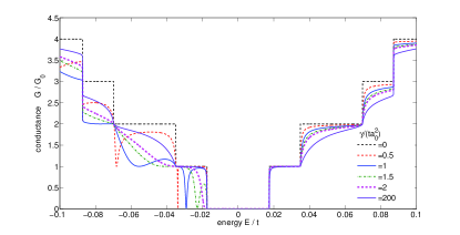
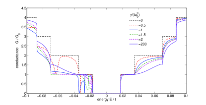
For the single -function impurity, as is shown in Fig. 2(a), we display the conductance in Fig. 3. Two main features are apparent in the figure. First, there are characteristic dips in the conductance for negative energies, where exactly one conductance quantum is lost. Secondly, the plateaux conductances exactly at the energies where new modes open appear to remain largely intact, especially on the positive energy side. The origin of all these features can be studied analytically.
We can write the -matrix asBergvallPRB2013
| (7) |
where the subscript and denotes evanescent and propagating modes, respectively, and
| (8) |
These functions depend on energy , the transverse eigenmodes at the location of the impurity ( is the ribbon width), and the magnitudes of the longitudinal momenta, defined as , where is the (quantized) transverse momentum in mode . That the evanescent modes actually have imaginary longitudinal wavevectors has been taken into account above.
From Eq. (7) it is clear that at the bottom of a subband , where the wave vector of the evanescent mode goes to zero, diverges and the T-matrix vanishes, since remains finite. Therefore, all conductance plateaux values at energies corresponding to the bottom of subbands remains intact for this type of impurity. Also, if the equation can be fulfilled, there is a posibility of a transmission resonance. Both results are analagous to the situation in the 1D quantum channel made from a 2DEG,Bagwell1 ; Bagwell2 where it was shown that the conductance steps are always present at the bottom of subbands and dips can occur when the impurity potential is attractive. In the case of graphene, the repulsive impurity corresponds to an attractive one on the hole-side of the spectrum (negative energies) and dips are found on that side. We note that if we change sign of , the whole picture in Fig. 3 is flipped .
To quantify the resonance behavior further, we keep one propagating mode denoted and one evanescent mode denoted and compute the position of the dip relative to the bottom of the evanescent subband . We obtain
| (9) |
It can be shown that at this energy, the scattering part of the propagator and the full propagator between source and drain vanishes and the contribution to the conductance from this channel is lost. For small the resonance is close to the conductance step, while for intermediate it can be located anywhere along the plateau. For very large , the dip merges with the step, but the effect discussed above for vanishing wins and the step structure remains intact. The conductance becomes symmetric as and there are no dips. The above formula is exact for the lowest open mode but should be corrected for higher modes. Depending on the value of some resonances are not perfect back-reflection resonances on higher plateaux, which is also clear from Fig. 3.
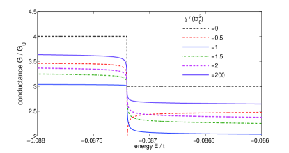
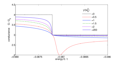
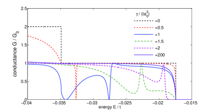
If we inspect Fig. 3 more carefully, we start to suspect that some steps are lost, for instance the one on the where the fourth mode opens. But if we zoom in and look carefully, as in Fig. 4, we see that the conductance at the point when the next higher lying subband (the fourth) is opened remains intact, although the recovery is very steep. Actually, this is accidental, in that the impurity position was chosen as . If we choose another impurity position, the transparency of the impurity and the conductance recovery is more clearly visible, see Fig. 5
III.2 A-B-site impurity
Next we consider the case of a scalar impurity in the sublattice space (diagonal potential), a situation corresponding to an impurity potential on two neighboring sites, as illustrated in Fig. 2(b). We display the conductance for varying impurity strengths in Fig. 6. As is clear from the figure, the situation is more complicated as compared with the A-site impurity. We zoom in on the structures around the first step in Fig. 7 and concentrate the discussion around this figure.
This case is unique to graphene and has no direct correspondence for a 1D channel made from a 2DEG. The off-diagonal components of the A-B sublattice matrix propagator ;E) enters directly in the -matrix equation. These components contain factors encoding the Dirac electron chirality, see Eqs. (B5)-(B10) in Ref. BergvallPRB2013, . The full analytic expression for the -matrix is rather lengthy and not so informative. Therefore, we write it in a short-hand notation to display its structure,
| (10) |
For instance, the function reduces to for the A-site impurity in Eq. (7) above. The function corresponds to interference between the A-site and B-site scattering events through the opportunity of changing sublattice. The -element of this -matrix can be rewritten as
| (11) |
It can be shown that
| (12) |
and the first fraction in will stay finite when a , while the second one will approach zero. Thus, the -matrix stays finite and we will not regain a perfect channel as as we did in the A-site impurity case. This is due to the extra freedom of changing sublattice during multiple scattering events at the A and the B site impurities. In addition to this, there are more degrees of freedom to aquire resonances in the -matrix which is apparent from the rich resonance structure in Fig. 7. In this case, both transmission dips (including a complete loss of a channel) and transmission resonance in the middle of the plateau (green dash-dotted line in the figure) can occur depending on the value of .
IV Summary
In summary, we have presented analytical results for electron transport in graphene nanoribbons with perfect armchair edges. We have shown how the interplay between evanescent waves around localized scattering centers and propagating waves connecting source and drain generates back-scattering resonances that result in dips in the transmission function. At the same time back-scattering is completely suppressed for the A-site impurity at energies corresponding to the bottom of subbands, where the conductance completely recovers. This is analagous to the case of 1D channels made from 2DEGs. However, for an A-B site impurity, multiple scattering at the double impurity includes intermediate A to B sublattice scattering that interfere with the transmission resonance and it is lost. We have derived a Fisher-Lee type expression relating the transmission to the electron propagator that can be used for further studies of more complicated scattering regions.
V Acknowledgements
This work has been supported by the Swedish Foundation for Strategic Research (SSF), Knut and Alice Wallenberg foundation (KAW), and the EU through the FP7 project ConceptGraphene.
Appendix A T-matrix equation
By looking at Fig. 1, we see that the propagator from to may be written as
| (13) |
where we have introduced the shorthand notation , and where corresponds to the process of the electron hopping from the impurity site , interacting with the impurity and then hopping back. In the process, the electron is scattered from mode to . If we assume that the potential does not depend on mode index or position, we have that . Still, the A-B sub lattice degree of freedom remains and is a matrix.
By observation, the expression for the propagator may be rewritten as
| (14) |
where the -matrix is
| (15) |
or,
| (16) |
Since there is no mode-dependence in the right-hand side, we can drop the mode-indices from the -matrix, and we arrive at the final expression,
| (17) |
Appendix B Derivation of a Fisher-Lee transport formula for graphene
In this appendix, we derive an expression relating the transmission function between graphene leads to the electron propagator (Green’s function) of the graphene scattering region connecting the leads together, as displayed in Fig. 8(a). When we need to be specific, we use the AGNR waveguide lead eigenfunctions which are known analytically, but the formalism can be generalized to other leads as long as one at least numerically can compute the lead eigenfunctions. Following Büttiker,ButtikerPRB1992 we denote by the probability of an electron wave incoming in lead in transverse mode , to exit through lead in transverse mode . We study only elastic scattering processes, and is thus the energy of both the incoming and outgoing waves.
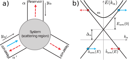
Using a local coordinate system in each lead, where is the transverse coordinate and the longitudinal one, increasing in the direction towards the scattering region, we write down the wavefunction of an electron in lead and transverse mode as
| (18) |
where the transverse wave functions for AGNRs are given by
| (19) |
where is the width of lead . The pseudo spinor is given by
| (20) |
Above, denotes an incoming or outgoing wave, as indicated in Fig. 8(b). The transverse momenta are defined as , while the longitudinal momenta are given by
| (21) |
where the Fermi velocity of pristine two-dimensional graphene, is the band bottom of mode , and is a possible shift of the Dirac point away from zero in lead by application of a back gate voltage, as also indicated in Fig. 8(b).
We introduce the operators and , that annihilates an incoming and outgoing states, respectively, in lead and mode (see Fig. 8b). The general scattering state in lead can then be written as
| (22) |
where is added to make sure that we only incorporate propagating transverse eigenmodes in the leads. The first and second step functions correspond to the electron bands (above the Dirac point) and hole bands (below the Dirac point), respectively
By definition, the retarded Green’s function, propagating an electron from lead to lead , is
| (23) |
Using Eq. (22), we find that
| (24) |
Next we need the commutation relations for the operators. First, we have
| (25) |
The outgoing waves are related to the incoming waves through the scattering matrix as
| (26) |
which leads to
| (27) |
and
| (28) |
By using these commutation relations, the expression for the propagator turns into
| (29) |
We multiply (29) by the transverse wavefunctions and from the left and right, respectively, and integrate the transverse coordinates and over the ribbon widths. We then kill the double sum over transverse modes leaving us with a propagator , for scattering from mode to .
For this stationary problem, we only have a dependence on time-difference. It is then natural to introduce and integrate over to obtain the Fourier-transform of the propagator, . Moving out factors not depending on in front of the integral, we get (leaving out the prefactor for now) the standard integral,
| (30) |
where is a small positive number.
At this point it is time to perform the integral over energy . Since the integrand has a single pole at in the upper complex half-plane, it is natural to move into the complex plane (), and integrate slightly above or below the -axis and close the contour either in the upper or lower half of the complex plane, depending on the convergence criterium on the closing arc at large distance , which is controlled by the signs of in the different terms. It turns out that only the last two terms in Eq. (29) will allow us to close the contour in the upper plane where the pole exists and only those two terms contribute. We obtain
| (31) |
We now have an expression relating the propagator to the -matrix, but we want the inverse relation. To obtain the -matrix we need to project with the ribbon pseudo-spinors, and divide down the prefactors. In that last step one can get rid of the spurious coordinate dependence in Eq. (31) by a subtle trick.FisherLee One needs to observe that the coordinate dependence of the propagator also is in the form of exponential functions, that exactly cancel the ones we divide down.111For our case of an AGNR with a defect being our system, this can be explicitly checked in our previous paperBergvallPRB2013 in Eqs. (B8)-(B9). This allows us to let and approach in their respective lead, with the added constraint that . This step properly identifies the -matrix as connecting ideal reservoirs in the far distance contacted to the scattering region through the ideal leads, in the spirit of the Landauer-Büttiker formalism. If the coordinate systems are aligned as shown in Fig. 9, we have to evaluate when and . Bringing it all together we introduce
| (32) |
We now get the final expression for the -matrix as
| (33) |
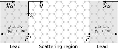
In summary, the general strategy is to compute the propagator for the scattering part between leads, then project as in Eq. (32) and use Eq. (33) to get the -matrix. In the main text of this paper we use the analytic form for the propagator for an AGNR with and without an impurity scattering center at , obtained in Ref. BergvallPRB2013, , together with the above results to obtain analytic formulas for the conductance.
References
- (1) A. G. Castro Neto, F. Guinea, N. M. R. Peres. K. S. Novoselov, and A.K. Geim, Rev. Mod. Phys. 81, 109 (2009)
- (2) N. Peres, Rev. Mod. Phys. 82, 2673 (2010)
- (3) K S Novoselov, V I Fal ko, L Colombo, P R Gellert, M G Schwab, and K Kim Nature 490, 192 (2012).
- (4) M. R. Connolly and C. G. Smith, Phols. Trans. R. Soc., A 368, 5379 (2010)
- (5) A. Deshpande and B. J. LeRoy, Phys. E (Amsterdam, Neth.) 44, 743 (2010)
- (6) M. Y. Han, B. Özyilmax, Y. Zhang, and P. Kim, Phys. Rev. Lett. 98, 206805 (2007).
- (7) L. C. Campos, V. R. Manfrinato, J. D. Sanchez-Yamagishi, J. Kong, and P. Jarillo-Herrero, Nano Lett. 9, 2600 (2009).
- (8) C. Ö. Girit, J. C. Meyer, R. Erni, M. D. Rossell, C. Kisielowski, L. Yang, C. H. Park, M. F. Crommie, M. L. Cohen, S. G. Louie, Science 323 1705 (2009).
- (9) J. Cai, P. Ruffieux, R. Jaafar, M. Bieri, T. Braun, S. Blankenburg, M. Muoth, A. P. Seitsonen, M. Saleh, X. Feng, K. Müllen, and R. Fasel, Nature 466, 470 (2010)
- (10) X. Li, X. Wang, L. Zhang, S. Lee, and H. Dai, Science 319, 1229 (2008)
- (11) F. Banhart, J. Kotakoski, and A. V. Krasheninnikov, ACS Nano, 5, 26 (2011).
- (12) H. Raza (editor), Graphene Nanoelectronics: Metrology, Synthesis, Properites and Applications (Springer-Verlag, Berlin, Heidelberg, 2012)
- (13) M.I. Katsnelson, Graphene: Carbon in Two Dimensions (Cambridge University Press, 2012)
- (14) L. E. F. Foa Torres, S. Roche and J.-C. Charlier Introduction to Graphene-Based Nanomaterials (Cambridge University Press, Cambridge, 2014).
- (15) D. S. Fisher and P. A. Lee, Phys. Rev. B 23, 6851 (1981).
- (16) P. F. Bagwell, Phys. Rev. B, 41, 10354 (1990).
- (17) P. F. Bagwell, J. of Phys.-Cond. Mat. 2, 6179 (1990).
- (18) T. O. Wehling, A. M. Black-Schaffer, and A. V. Balatsky, arXiv:1405.5774 [cond-mat.mtrl-sci] (2014).
- (19) V. P. Gusynin and S. G. Sharapov, Phys. Rev. Lett. 95, 146801 (2005)
- (20) N. M. R. Peres, F. Guinea, and A. H. Castro Neto, Phys. Rev. B 73, 125411 (2006).
- (21) T. Löfwander and M. Fogelstrom, Phys. Rev. B, 76, 193401 (2007).
- (22) A. Bergvall and T. Löfwander, Phys. Rev .B 87 205431 (2013).
- (23) For a review see S. Datta, Electronic Transport in Mesoscopic Systems (Cambridge University Press, Cambridge, UK, 1997).
- (24) J. Tworzydlo, B. Trauzettel, M. Titov, A. Rycerz, and C. W. J. Beenakker, Phys. Rev. Lett. 96, 246802 (2006)
- (25) M. Büttiker, Phys. Rev. B 46, 12485 (1992).