Undoped accumulation-mode Si/SiGe quantum dots
Abstract
We report on a quantum dot device design that combines the low disorder properties of undoped SiGe heterostructure materials with an overlapping gate stack in which each electrostatic gate has a dominant and unique function — control of individual quantum dot occupancies and of lateral tunneling into and between dots. Control of the tunneling rate between a dot and an electron bath is demonstrated over more than nine orders of magnitude and independently confirmed by direct measurement within the bandwidth of our amplifiers. The inter-dot tunnel coupling at the charge configuration anti-crossing is directly measured to quantify the control of a single inter-dot tunnel barrier gate. A simple exponential dependence is sufficient to describe each of these tunneling processes as a function of the controlling gate voltage.
Silicon-based quantum devices hold great promise for realizing spin qubits.Zwanenburg et al. (2013) The ability to isotopically purify silicon has resulted in the demonstration of extremely long spin-coherence times in donor-based silicon devicesZwanenburg et al. (2013); Muhonen et al. (2014) and in recent years a series of results have demonstrated many fundamental properties of electrostatically-defined silicon-based quantum devices. Measurements of ,Hayes et al. (2009); *Xiao2010PRL; *Simmons2011 valley splitting,Shi et al. (2011); Prance et al. (2012) and Pauli blockadeShaji et al. (2008); Prance et al. (2012) were made using doped depletion-mode SiGe devices. Improved device performance was achieved by eliminating the intentional dopants in the SiGe heterostructure, a major source of noise and instability, making necessary the use of a global field gate to accumulate electrons. This allowed for demonstrations of high mobility two-dimensional electron gases (2DEGs),Lu et al. (2009) Coulomb blockade,Lu et al. (2011) valley splitting,Xiao, House, and Jiang (2010b) Pauli blockade,Borselli et al. (2011a)and and Rabi measurements.Maune et al. (2012)
The ideal realization of electrostatically-defined quantum dot devices would have independent control of the charge occupancy of each dot and its associated exchange couplings. A promising approach is to utilize an accumulation-based design in which independent localized gates are used to create electron baths, create and control quantum dot occupancy, and modulate tunnel barriers between them. A Si metal-oxide-semiconductor based design has shown great promise along these lines, demonstrating in quick succession charge sensing,Yang et al. (2011, 2012) valley splitting,Lim et al. (2011) and well-controlled double-dot behavior including spin blockade.Lai et al. (2011) However better isolation from residual disorder due to gate oxide charges can potentially be achieved using a SiGe heterostructure.
In this Letter we report on a double quantum dot device with an integrated dot charge sensor based on a synthesis of the improved gated control of the accumulation-mode designsLai et al. (2011) with the lower disorder of field-gated SiGe heterostructure designs.Borselli et al. (2011a) This approach builds on our previous experience with quantum devices made using single gates in accumulation modeCroke et al. (2010); Borselli et al. (2011b) and achieves the goal of complete gated control over a set of quantum dots and inter-dot couplings, dominating over the effects of disorder.
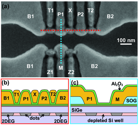
A nominally undoped epitaxial heterostructure similar to that previously reported by our groupBorselli et al. (2011a) produces a tensily-strained Si quantum well on a strain-relaxed buffer. Alternating depositions of dielectric and metal are patterned via electron-beam lithography to create an overlapping set of highly localized gates along the edge of, and adjacent to, a low- dielectric spin-on glass (SOG).Wolf and Tauber (1986) Shown schematically in Fig. 1, these gates can be operated in forward bias to locally control the creation of 2DEG baths (B1 and B2) and quantum dots (P1, P2, and M), and the intervening tunnel barriers (T1, X, T2, Z1, and Z2). Each of the non-bath gates have leads that enter the central device area on top of the SOG. The lower capacitance of these leads results in a higher threshold voltage, preventing charge accumulation in the quantum well except under the tips of the gates that touch down closer to the epitaxial layers.
An integrated quantum dot charge sensor is formed by biasing the lower set of gates (B1, Z1, M, Z2, B2) such that a few-electron dot is created under gate M that is strongly tunnel coupled to 2DEGs formed under bath gates B1 and B2, with nominal electron densities . The voltage on M is first set to the few-electron regime (based on the threshold voltage of a large-area Hall bar) and the tunnel barrier gates, Z1 and Z2, are adjusted to create symmetric tunneling rates between the sensing dot (M-dot) and the 2DEGs. The voltage on M is then set to the edge of a Coulomb blockade peak where is at a maximum.Barthel et al. (2010); Nordberg et al. (2009) The charge sensitivity is determined by the ratio of the P- to M-dot mutual capacitance, , to the product of their total capacitances as .Nordberg et al. (2009) These devices have a typical maximum sensitivity of .
In order to probe the device electrostatics over a large range of bias space with constant sensitivity, the chemical potential of the M-dot is held approximately fixed. For small changes in the voltage on M, the gain is constant allowing measurement of the capacitive ratios of the P, T, and X gates to the chemical potential of the M-dot. These provide linear voltage corrections to which are used in a software-controlled open-loop feedback to straightforwardly hold fixed the chemical potential of the sensing dot as the other gate voltages are varied.
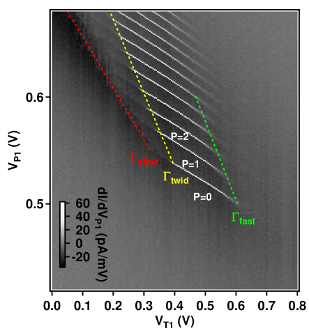
Charge stability diagrams of quantum dots formed under the plunger gates, P1(2), are generated by sweeping the DC biases, , versus a respective neighboring tunnel barrier gate voltage, . Figure 2 shows an example (from a device loaded in a – dilution refrigerator with a base temperature of ) generated by applying a small-amplitude, , square wave at to the P1 gate and recording the differential transconductance with standard lock-in techniques. In the region between the red and yellow lines, the tunneling rate into the dot is slower than the gate pulse twiddle frequency,Elzerman et al. (2004) , but faster than the sweep rate of per column of data. Between the yellow and green lines, the tunneling rate into the P1-dot becomes faster than the gate pulse twiddle frequency, , resulting in stable charge transition boundaries. For values of to the right of the green line, the tunneling rate into the dot exceeds that associated with the peak-to-peak amplitude of the square pulse applied to P1, , resulting in lifetime broadening of the transition lines. The ratio of the rates is , and furthermore, the observation of single shot events down to the scan rate, , means that the T1 gate is controlling the dot-to-bath tunnel rate by well over nine orders of magnitude.
The relative capacitances of the P1 and T1 gates to the quantum dot are not changing, i.e., the iso-occupancy lines are straight, indicating that the position of the centroid of the dot wavefunction in the 2DEG remains approximately fixed. The absence of other transitions or inflections indicates a system with low disorder, and this stability allows the simple open-loop feedback control to maintain constant sensitivity for hours. An advantage of this accumulation-mode design over previous workBorselli et al. (2011a) is the marked decrease in cross-capacitance between adjacent gates. In depletion-mode designs it is not uncommon for several gates to have comparable capacitances to the dot chemical potential of interest.Hanson et al. (2007) By accumulating charge under a single gate, as is done here, the capacitive ratios of the adjacent gates are significantly reduced. The largest cross-capacitance term for any quantum dot in this device is from its adjacent tunnel barrier gate and is of order twenty percent (slope of charge transition boundaries in Fig. 2).
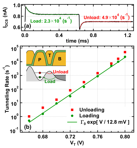
A quantitative analysis of the dot-to-bath tunneling rates was obtained from a second similar device loaded in a 3He refrigerator with a base temperature of and tuned to a comparable configuration. The loading and unloading rates of the first electron as a function of the tunnel barrier gate bias, , were measured by applying a fixed amplitude square pulse to the plunger gate. 111Independent excited-state-spectroscopy measurementsElzerman et al. (2004) and magneto-spectroscopyBorselli et al. (2011b); Yang et al. (2012); Shi et al. (2011) confirmed that this pulse amplitude was large enough to indiscriminately load into both ground and excited valley states. The pulse durations were varied to be approximately one order of magnitude longer than the measured rates. For each value of , both and were linearly compensated to hold the chemical potentials of the P- and M-dots approximately fixed with respect to the 2DEG. The charge sensor currents were recorded (averaged over 7,800 time traces in Fig. 3(a)) and fit to exponential time decays to extract the average loading and unloading rates. The resulting tunneling rates, plotted in Fig. 3(b) as a function of T gate voltage, have a simple exponential dependence over nearly five orders of magnitude. Simulations of these device designs confirm that, under the conditions of these experiments, the dominant influence of the T gate is to modulate the strength of the potential barrier between the dot and 2DEG, resulting in the observed exponential dependence on gate voltage. The unloading rate is always faster than the loading rate over the entire range, as is expected due to the smaller tunnel barrier in the unloading configuration.Thalakulam et al. (2011)
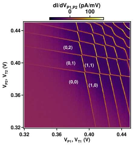
Figure 4 shows a charge stability diagram as a function of the voltages on gates P1 and P2, demonstrating the formation of a well-behaved double quantum dot. The dot-to-bath tunneling rates have been held approximately fixed by linearly compensating with voltages and . The inter-dot tunnel coupling is being allowed to change as we are holding the X-gate voltage fixed. The observed increase in tunnel coupling towards the upper right of the figure is due to the small cross-capacitance of the P1(2) gates to the inter-dot potential barrier; therefore increasing positive bias on the P gates lowers the tunnel barrier with respect to the Fermi level. We are confident in the attributed charge configurations as no evidence of further transitions is seen along the respective first electron loading lines while maintaining barrier transparency.
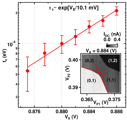
Finally we demonstrate control of the inter-dot tunnel coupling at the charge transition. Larger values of tunnel coupling can be measured directly from the curvature of charge state boundaries at the triple points of a charge stability diagram.Hanson et al. (2007) In Fig. 5 we plot the tunnel coupling extracted from versus charge stability diagrams like that shown in the inset. For each fixed X-gate voltage we map the charge sensor current while sweeping the P1 and P2 gates. The charge sensor voltage, , is compensated to maximize sensitivity to changes in total charge resulting in no observable differential charge sensitivity between the and charge configurations. This technique maximizes the contrast of the net-charge boundaries allowing measurement of down to . The tunnel coupling is highly controllable and follows a similar simple exponential dependence on the controlling gate voltage as was found for the dot-to-bath tunnel coupling. A similar exponential dependence of the inter-dot tunnel coupling on a controlling gate voltage has been reported previously in a SiGe depletion-mode double quantum dot.Simmons et al. (2009)
We have demonstrated the basic operation of SiGe quantum dot devices that use overlapping gates to individually control electron occupancy and lateral tunneling. The electron tunneling rates between quantum dots and adjacent electron baths, and between pairs of quantum dots exhibit a simple exponential dependence on a single controlling gate voltage. The variation of the dot-to-bath tunneling rate has been shown to be controllable over at least nine orders of magnitude. This device design, utilizing an undoped SiGe heterostructure and operated in an all-accumulation-mode, achieves robust gated electrostatic control of few-electron systems in an inherently low-disorder environment.
Sponsored by United States Department of Defense. The views and conclusions contained in this document are those of the authors and should not be interpreted as representing the official policies, either expressly or implied, of the United States Department of Defense or the U.S. Government. Approved for public release, distribution unlimited.
References
- Zwanenburg et al. (2013) F. A. Zwanenburg, A. S. Dzurak, A. Morello, M. Y. Simmons, L. C. L. Hollenberg, G. Klimeck, S. Rogge, S. N. Coppersmith, and M. A. Eriksson, Rev. Mod. Phys. 85, 961 (2013).
- Muhonen et al. (2014) J. T. Muhonen et al., (2014), arXiv:1402.7140v1 [cond-mat] .
- Hayes et al. (2009) R. Hayes et al., (2009), arXiv:0908.0173v1 [cond-mat] .
- Xiao, House, and Jiang (2010a) M. Xiao, M. G. House, and H. W. Jiang, Phys. Rev. Lett. 104, 096801 (2010a).
- Simmons et al. (2011) C. B. Simmons, J. R. Prance, B. J. V. Bael, T. S. Koh, Z. Shi, D. E. Savage, M. G. Lagally, R. Joynt, M. Friesen, S. N. Coppersmith, and M. A. Eriksson, Phys. Rev. Lett. 106, 156804 (2011).
- Shi et al. (2011) Z. Shi, C. B. Simmons, J. R. Prance, J. K. Gamble, M. Friesen, D. E. Savage, M. G. Lagally, S. N. Coppersmith, and M. A. Eriksson, Appl. Phys. Lett. 99, 233108 (2011).
- Prance et al. (2012) J. R. Prance, Z. Shi, C. B. Simmons, D. E. Savage, M. G. Lagally, L. R. Schreiber, L. M. K. Vandersypen, M. Friesen, R. Joynt, S. N. Coppersmith, and M. A. Eriksson, Phys. Rev. Lett. 108, 046808 (2012).
- Shaji et al. (2008) N. Shaji, C. B. Simmons, M. Thalakulam, L. J. Klein, H. Qin, H. Luo, D. E. Savage, M. G. Lagally, A. J. Rimberg, R. Joynt, M. Friesen, R. H. Blick, S. N. Coppersmith, and M. A. Eriksson, Nature Physics 4, 540 (2008).
- Lu et al. (2009) T. M. Lu, D. C. Tsui, C.-H. Lee, and C. W. Liu, Appl. Phys. Lett. 94, 182102 (2009).
- Lu et al. (2011) T. M. Lu, N. C. Bishop, T. Pluym, J. Means, P. G. Kotula, J. Cederberg, L. A. Tracy, J. Dominguez, M. P. Lilly, and M. S. Carroll, Appl. Phys. Lett. 99, 043101 (2011).
- Xiao, House, and Jiang (2010b) M. Xiao, M. G. House, and H. W. Jiang, Appl. Phys. Lett. 97, 032103 (2010b).
- Borselli et al. (2011a) M. G. Borselli, K. Eng, E. T. Croke, B. M. Maune, B. Huang, R. S. Ross, A. A. Kiselev, P. W. Deelman, I. Alvarado-Rodriguez, A. E. Schmitz, M. Sokolich, K. S. Holabird, T. M. Hazard, M. F. Gyure, and A. T. Hunter, Appl. Phys. Lett. 99, 063109 (2011a).
- Maune et al. (2012) B. M. Maune, M. G. Borselli, B. Huang, T. D. Ladd, P. W. Deelman, K. S. Holabird, A. A. Kiselev, I. Alvarado-Rodriguez, R. S. Ross, A. E. Schmitz, M. Sokolich, C. A. Watson, M. F. Gyure, and A. T. Hunter, Nature 481, 344 (2012).
- Yang et al. (2011) C. H. Yang, W. H. Lim, F. A. Zwanenburg, and A. S. Dzurak, AIP Adv. 1, 042111 (2011).
- Yang et al. (2012) C. H. Yang, W. H. Lim, N. S. Lai, A. Rossi, A. Morello, and A. S. Dzurak, Phys. Rev. B 86, 115319 (2012).
- Lim et al. (2011) W. H. Lim, C. H. Yang, F. A. Zwanenburg, and A. S. Dzurak, Nanotechnology 22, 335704 (2011).
- Lai et al. (2011) N. S. Lai, W. H. Lim, C. H. Yang, F. A. Zwanenburg, W. A. Coish, F. Qassemi, A. Morello, and A. S. Dzurak, Sci. Rep. 1, 110 (2011).
- Croke et al. (2010) E. T. Croke, M. G. Borselli, M. F. Gyure, S. S. Bui, I. I. Milosavljevic, R. S. Ross, A. E. Schmitz, and A. T. Hunter, Appl. Phys. Lett. 96, 042101 (2010).
- Borselli et al. (2011b) M. G. Borselli, R. S. Ross, A. A. Kiselev, E. T. Croke, K. S. Holabird, P. W. Deelman, L. D. Warren, I. Alvarado-Rodriguez, I. Milosavljevic, F. C. Ku, W. S. Wong, A. E. Schmitz, M. Sokolich, M. F. Gyure, and A. T. Hunter, Appl. Phys. Lett. 98, 123118 (2011b).
- Wolf and Tauber (1986) S. Wolf and R. N. Tauber, Silicon Processing for the VLSI Era, Vol. 1: Process Technology (Lattice Press, Sunset Beach, CA, 1986).
- Barthel et al. (2010) C. Barthel, M. Kjærgaard, J. Medford, M. Stopa, C. M. Marcus, M. P. Hanson, and A. C. Gossard, Phys. Rev. B 81, 161308 (2010).
- Nordberg et al. (2009) E. P. Nordberg, H. L. Stalford, R. Young, G. A. T. Eyck, K. Eng, L. A. Tracy, K. D. Childs, J. R. Wendt, R. K. Grubbs, J. Stevens, M. P. Lilly, M. A. Eriksson, and M. S. Carroll, Appl. Phys. Lett. 95, 202102 (2009).
- Elzerman et al. (2004) J. M. Elzerman, R. Hanson, L. H. W. van Beveren, L. M. K. Vandersypen, and L. P. Kouwenhoven, Appl. Phys. Lett. 84, 4617 (2004).
- Hanson et al. (2007) R. Hanson, L. P. Kouwenhoven, J. R. Petta, S. Tarucha, and L. M. K. Vandersypen, Rev. Mod. Phys. 79, 1217 (2007).
- Note (1) Independent excited-state-spectroscopy measurementsElzerman et al. (2004) and magneto-spectroscopyBorselli et al. (2011b); Yang et al. (2012); Shi et al. (2011) confirmed that this pulse amplitude was large enough to indiscriminately load into both ground and excited valley states.
- Thalakulam et al. (2011) M. Thalakulam, C. B. Simmons, B. J. V. Bael, B. M. Rosemeyer, D. E. Savage, M. G. Lagally, M. Friesen, S. N. Coppersmith, and M. A. Eriksson, Phys. Rev. B 84, 045307 (2011).
- Simmons et al. (2009) C. B. Simmons, M. Thalakulam, B. M. Rosemeyer, B. J. V. Bael, E. K. Sackmann, D. E. Savage, M. G. Lagally, R. Joynt, M. Friesen, S. N. Coppersmith, and M. A. Eriksson, Nano Lett. 9, 3234 (2009).