Polariton-based optical switch
Abstract
Based on the studies of propagation of an exciton-polariton condensate in a patterned optical microcavity with an embedded graphene layer, we propose a design of a Y-shaped electrically-controlled optical switch. The polaritons are driven by a time-independent force due to the microcavity wedge shape and by a time-dependent drag force owing to the interaction of excitons in graphene and the electric current running in a neighboring quantum well. It is demonstrated that one can control the polariton flow direction by changing the direction of the electric current. The simulations also show that an external electric field normal to the microcavity plane can be utilized as an additional parameter that controls the propagation of the signals in the switch. By considering the transient dynamics of the polariton condensate, we estimate the response speed of the switch. Finally, we propose a design of the polariton switch in a flat microcavity based on the geometrically identical Y-shaped quantum well and graphene pattern where the polariton flow is only induced by the drag force.
I Introduction
In the past decades, substantial experimental and theoretical efforts were devoted to find the optimal ways to tune the optical properties of semiconductors and graphene by application of external electric and magnetic fields. The motivation of this research lies in the potential applications for integrated circuits in optical and quantum computers, for secure information transfer, and in new light sources.Gibbs et al. (2011) One of the promising approaches is in the use of polaritons, which are a quantum superposition of cavity photons and excitons in a nanometer-wide semiconductor layer (a quantum well) or graphene.Zamfirescu et al. (2002); Deng et al. (2002); Liew et al. (2010); Menon et al. (2010); Deng:10 ; Berman et al. (2012a) Since polaritons are interacting Bose particles, a polariton gas can transit to a superfluid state that, under certain conditions, propagates in a microcavity almost without dissipation.Carusotto and Ciuti (2004); Amo et al. (2009a); Wouters and Savona (2010); Berman et al. (2012a) Due to a small effective mass, of the free electron mass, the superfluid transition occurs at relatively high temperatures that are comparable with the room temperature. Polaritons can propagate in the sample with a speed up to a few percent of the speed of light that is, much faster than that of electric-field driven electrons and holes in semiconductors.Wouters and Carusotto (2010) However, one of the main problems to be solved in actual design of polariton-based optical devices is in weak response of polaritons to an external electric field owing to their net zero electric charge.

In this paper, we propose a design of polariton-based, electrically controlled switch, in which the polariton propagation is controlled by means of a drag force. Recently, it was shown that the drag caused by an electric current results in entrainment of polaritons and in formation of a persistent, directed polariton current in the microcavity.Berman et al. (2010a, b) In this case, this is a drag force that is exerted on the exciton component of polaritons that results in generation of the polariton flux proportional to the driving electric field ,
| (1) |
where is the temperature-dependent drag coefficient. In addition to the electrically controlled drag force, the polaritons can also be accelerated by a constant, time independent force, which is caused by the wedge-like shape of the microcavity.Sermage et al. (2001); Nelsen et al. (2013) In the latter case, the effect of the constant force is similar to application of a dc voltage in electric circuits. By changing the magnitude and direction of the electric current one can vary the net force exerted on the polaritons and thus, to control the polariton propagation.
In this paper, we propose the polariton switches of two types. In the first design, the polariton flow in the switch is produced by a constant force due to the wedge-like shape of the microcavity whereas the drag force is utilized to switch the direction of the flow. In the second design, the polariton flow in the required direction is only produced by the drag force. The photons propagate in the planar microcavity, and the excitons are located in a quantum well embedded in the microcavity. Below we describe the both types of the switches in details.
In the first design, we take advantage of a patterned microcavity to create a potential-energy landscape for polaritons in the form of one-dimensional channels, or “polariton wires”, which are somewhat similar to the ordinary wires that conduct electrical current. However, in our case, the wires conduct polaritons and help one to deliver photons to a desired location in the semiconductor structure. Recently developed experimental techniques, which enable one to produce such guiding potentials for polaritons, include deposition of a metal pattern on the Bragg reflectorsUtsunomiya et al. (2008) and modulation of the cavity layer thickness in a mesa structure.Daïf et al. (2006); Kaitouni et al. (2006) The polariton channels of complex shape and topology can also be engineered directly in an air-filled microcavity by creating quasi-one-dimensional waveguides, or micropillars.Wertz et al. (2010); Van Vugt et al. (2011); Nguyen et al. (2013); Das et al. (2013); Boulier et al. (2014)
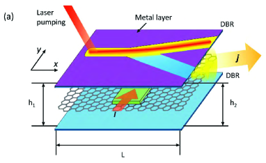
To design a polariton switch, we utilize a Y-shaped channel shown in Fig. 1. We assume that polaritons are created at a constant rate by the external laser pumping at the stem of the channel and then, propagate towards the junction under the action of a constant force due to the microcavity wedge-like shape. After reaching the junction, the polariton flow splits between the two branches. If no drag force is applied to the polaritons, the flux is distributed equally between the branches. However, if the drag force is exerted on the polaritons in the region of the junction in the direction normal to the stem, the polaritons are “pushed” towards one branch and hence, the flux in that branch increases. Simultaneously, the flux through another branch decreases due to approximate conservation of the total number of polaritons and in effect, the polariton flux is redistributed between the branches. The drag force in the junction region is produced by the electric current running in a neighboring quantum well, which has a form of a stripe placed in a microcavity perpendicular to the stem of the channel. Thus, the heterostructure encompasses two parallel quantum wells, separated by a nanometer-wide semiconductor of dielectric barrier, placed in an optical microcavity. Heterostructures embedded in a microcavity are widely used in the studies of exciton dynamicsBalili et al. (2009); Butov (2003) and in experiments with polaritons.Lai et al. (2007); Aßmann et al. (2011); Das et al. (2013) We demonstrate below that more than 70% of the total polariton flux can be dynamically redistributed between the branches for realistically achievable drag forces.
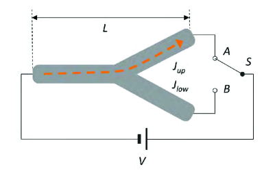
The second type of the polariton switch is based on a flat microcavity where the mirrors are parallel to each other. In this design, the excitons are located in a Y-shaped semiconductor quantum well, and the neighboring current-carrying quantum well geometrically repeats the shape of the structure, see Fig. 2. In contrast to the first type of the switch described above, here we do not use the patterned microcavity. Instead, the polaritons are guided by the Y-shaped semiconductor structure. The electric current in the quantum well is generated by the external voltage. The drag force exerted on the cavity polaritons by the electric current is directed parallel to the channel and induces the polariton flow along one of the branches. The polariton flow is redistributed between the branches in response to switching of the electric voltage applied to the current-carrying quantum well.
In both designs, the quantum wells containing the excitons can be fabricated by using a number of materials, including GaAs,Balili et al. (2009); Butov (2003) CdTe,Kasprzak et al. (2006) WSe2,Wu et al. (2014) and gapped graphene.Furchi et al. (2012); Youngblood et al. (2014) While the polariton condensate was experimentally observed when the polaritons are formed by excitons in a semiconductor quantum well Deng:10 , in this paper we focus on microcavity polaritons formed by excitons in graphene. One of the advantages to use graphene is related to the properties of polaritons in gapped graphene that can be tuned by application of a static electric field normal to the microcavity plane. Specifically, the energy gap between the valence and conduction bands can be created and changed by the electric field in a wide range.Kuzmenko et al. (2009); Mak et al. (2009); Zhang et al. (2009) This enables one to tune the polariton effective mass and the sound velocity in the spectrum of the quasiparticles Berman et al. (2010c) and through that to optimize the performance of the system, as detailed below. Another advantage of considering excitons in a graphene layer compared to a semiconductor quantum well is the absence of the fluctuations of the width due to the fact that graphene is a 2D one atom-thick material. Such fluctuations cause the disorder which results to the decrease of the drag coefficients due to the scattering of the excitons on the random field. Thus, in both designs of the polariton switch described above we consider graphene embedded in microcavity. Our consideration of the switch with polaritons formation in a quantum well currently is in progress.
II The dynamics of a polariton condensate
The dynamics of the polariton condensate was captured via the non-equilibrium Gross-Pitaevskii equation for the condensate wave function Carusotto and Ciuti (2013)
| (2) | |||||
where is the polariton mass, is a two-dimensional vector in the plane of the microcavity, and time , is the polariton-polariton interaction strength, is the polariton lifetime, and the source terms describes incoherent laser pumping of the polariton reservoir. In our simulations, we set ps as a representative value.Amo et al. (2009b); Nelsen et al. (2013)
The effective potential for the polaritons
| (3) |
is the sum of the confining potential owing to microcavity patterning , a linear potential corresponding to a constant accelerating force in a wedge-shaped microcavity , and a time-dependent drag caused by the driving electric current. The confining potential that forms the Y-shaped channel is shown in Fig. 1b. The potential depth compared to zero value outside the waveguide is taken equal 1 eV that is a representative value for waveguides in the microcavities.Utsunomiya et al. (2008); Daïf et al. (2006); Kaitouni et al. (2006) The average force acting upon a polariton wave packet in a wedge-shaped microcavity is , where is the energy of the polariton band taken at the in-plane wavevector of the polariton . For the wedge-like microcavity considered in this paper, the energy is a linear function of the spatial coordinateSermage et al. (2001); Nelsen et al. (2013) thus, the force is coordinate-independent. The corresponding potential is
| (4) |
where , and we suppose that the force is applied in -direction, along the stem of the Y-shaped channel.
The potential that described the drag force in -direction is taken equal
| (5) |
in a stripe 400 m m and otherwise. The drag force exerted on polaritons by charges moving in a neighboring quantum well is estimated in the -approximation as , where is the average gain of the linear momentum of polaritons owing to the drag, is the polariton momentum relaxation time, is a time-dependent electric field applied in the plane of the quantum well with free electrons, is the density of the normal component in a polariton superfluid,Berman et al. (2012b) is the Riemann zeta function, is the spin degeneracy factor, is the Boltzmann constant, is temperature, and is the sound velocity in the polaritonic system. By taking the polariton condensate density m-2, the separation between the graphene layer with the excitons and the quantum well with the electrons , (Vs)-1 and the relaxation time s as representative parameters for temperature K,Zinov’ev et al. (1983); Takagahara (2003); Basu and Ray (1991); Berman et al. (2010b) one obtains the maximum drag force meV/mm for the working range of electric fields mV/mm. In the simulations, we varied the maximum drag force from 1 to 4 meV/mm.
Formation of the excitons in graphene requires a gap in the electron and hole excitation spectra, which can be created and dynamically tuned by applying an external electric field in the direction normal to the graphene layer.Kuzmenko et al. (2009); Mak et al. (2009); Zhang et al. (2009) The gap can also be opened by chemical doping of graphene.Haberer et al. (2010) The polariton mass and the interaction strength in gapped graphene depend on the gap energy . The polariton effective mass in gapped graphene isBerman et al. (2012a)
| (6) |
where is the exciton effective mass in graphene, is the length of the microcavity, is the dielectric constant of the microcavity, and is the speed of light in vacuum. In the simulations, we set for a GaAs-based microcavity.Berman et al. (2010b) We consider the case of zero detuning where the cavity photons and the excitons in graphene are in resonance at . In this case the length of the microcavity isBerman et al. (2012a)
| (7) |
where , , is the permittivity of free space, and m/s is the Fermi-velocity of the electrons in graphene. The parameter is found from the equation
| (8) |
where . For dipolar excitons in GaAs/AlGaAs coupled quantum wells, the energy of the recombination peak is eV Negoita et al. (1999). We expect similar photon energies in graphene. However, its exact value depends on the graphene dielectric environment and substrate properties. The exciton effective mass in Eq. (6) isBerman et al. (2012a)
| (9) |
The polariton-polariton interaction strength is Berman et al. (2012a); Ciuti et al. (2003)
| (10) |
where is the two-dimensional Bohr radius of the exciton, is the exciton reduced mass.
III Results and discussion
III.1 Electrically controlled optical switch in a wedge-shaped microcavity
We study propagation of the polariton condensate in a patterned microcavity by numerically integrating the non-equilibrium Gross-Pitaevskii equation (2) for the wave function of the polariton condensate in the microcavity. In the model that is described in details in Sec. II we we determine the conditions that enable one to control the polariton spreading in a potential landscape.
The layered semiconductor structure considered in this section is shown in Fig. 1a. The excitons are positioned in the graphene layer whereas the free electrons are located in the neighboring, parallel quantum well. The heterostructure is placed between two high-quality multilayer mirrors (distributed Bragg reflectors, or DBR). In what follows, we consider a microcavity decorated with a Y-shaped pattern. Fig. 1b demonstrates the potential-energy landscape for the polaritons due to patterning of the microcavity. Additionally, the reflectors form a wedge opened towards the positive direction of the -axis (that is, to the right in Fig. 1) that results in a constant force exerted on the polaritons in a microcavity, as explained in Sec. II. In the simulation, we set the constant force equal meV/mm that corresponds to a representative experimental value.Sermage et al. (2001); Nelsen et al. (2013) The polaritons are created by an external laser radiation in the region of the stem. In what follows, an excitation spot has a Gaussian profile with a full width at half maximum (FWHM) of 65 m, centered in the stem part of the channel at m.
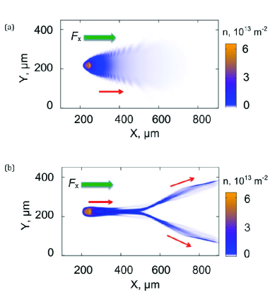
The effect of patterning on the polariton condensate propagation is shown in Fig. 3. It is seen that without the pattern (that is, without the confining potential in the plane), a polariton condensate driven by the constant force forms a wide trail in the direction of the force with the length of m. At larger distances from the excitation spot the condensate density rapidly decreases due to finite lifetime of polaritons. Propagation of the condensate under the same conditions in the presence of a Y-shaped pattern is shown in Fig. 3b. As is seen in this Figure, the polariton flow propagating in the patterned microcavity is localized in the channel formed by the pattern. In the region of the junction m, the polariton condensate flow splits between the “upper” and “lower” branches of the Y-channel. The polariton density in the channel at large distances m from the source is significantly higher than that in the microcavity without the channel (cf. Fig. 3a and b). The increase of the polariton density is caused by the confining potential that prevents the polariton flow from spreading in the plane.
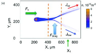
To probe the effect of the drag force on the polariton flow redistribution between the branches, in addition to the constant force we applied the force directed in -direction in a stripe 400 m m in the region of the junction. In Fig. 4a the area, in which the drag force is exerted, is bounded by the dashed lines. We found in the simulations that, due to the drag, the polaritons tend to propagate in the channel in the direction of the drag force and therefore, they mostly move in the upper branch of the channel in Fig 4a. To characterize the redistribution of the polaritons between the upper and lower branches we calculated the total polariton flux propagating in the branch,
| (11) |
where is the component of the polariton flux density parallel to the channel, is a unit vector along the branch, and
| (12) |
is the flux density.Messiah (1961) We integrate in Eq. (11) over the cross section of the branch. The flux was calculated at m that is, at a distance from the junction much larger than the width of the channel m.
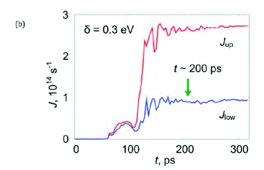
Fig. 4b shows the dependencies of the total polariton flux trough the upper (red curve) and lower (blue curve) branches as functions of time . In these simulations, the energy gap in the graphene quasiparticle excitation spectrum is set eV, the drag force is meV/mm, and the polariton source is turned on at the moment . According to the results shown in Fig. 4b, the polaritons propagate to the point at ps after the source is turned on. During the time interval 70 ps ps the polariton flux exhibits transient oscillations and then, tends to a constant value at ps. As it follows from Fig. 4b, the flux through the upper branch of the channel in the steady state is s-1, that is larger than that through the lower branch. Therefore, the polariton flow is redistributed among the branches in response to the drag force owing to the external, driving electric current. To quantify the redistribution of the polariton flux in the channel, we studied the dependence of the flux on the drag force . In the simulations, we varied from 1 meV/mm to 4 meV/mm, as explained in Sec. II. It is shown in Fig. 5a that the flux in the upper branch gradually increases with the rise of the drag force . In its turn, the flux through the lower channel, decreases thus, the total flux remains approximately constant. To more fully characterize the polariton flow in the channel, we determined the performance of the system,
| (13) |
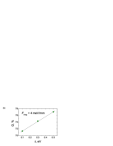
as a function of the energy gap in the graphene layer. We varied the gap from 0.1 to 0.5 eV that corresponds to the experimentally accessible range.Kuzmenko et al. (2009); Mak et al. (2009); Zhang et al. (2009); Haberer et al. (2010) The results for the constant drag force meV/mm are summarized in Fig. 5b. It is seen that the performance can be approximated by a linear function of the gap and it reaches % for the maximum gap eV. In other words, more than of the total polariton flux propagates through the upper channel for meV/mm, and less than of the flux only propagates through the lower channel.
Summarizing, we demonstrated that one can govern the propagation of a polariton condensate in the Y-shaped channel by means of the external electric current running in a neighboring quantum well. This make it possible to construct an optical, polariton-based switch controlled by an external voltage.
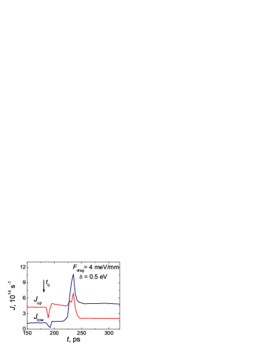
Finally, to estimate the response speed of the system, we studied the transient dynamics of a polariton condensate in the channel when the direction of the driving current is inverted. In these simulations, we turned on the pumping and waited ps until the system reached an equilibrium in the presence of a drag force. In this steady state, the polaritons mostly propagated in the upper channel, in accordance with our previous consideration. At ps, we changed the direction of the drag force to opposite. Since the drag force now pushes the polaritons down in the junction area, the polaritons tend to propagate via the lower channel, whereas the flux through the upper channel now decreases. After the transient oscillations were damped, the system came to a new equilibrium state where most of the polaritons propagated through the lower channel. The dependencies of the polariton fluxes and on time are shown in Fig. 6. According to this Figure, the characteristic switching time of the system between the states where the polaritons propagate via the upper and lower branches is ps. This means that the maximum switch frequency for this junction can reach GHz at given linear dimensions of the system. This frequency, however, should rise with decreasing channel length. In this paper we only consider the switch of length m and defer the size-dependent effects to the future studies.

III.2 Polariton switch in a flat microcavity
We now consider another design of the polariton switch based on the drag effect. In this case, the reflectors are parallel to each other. In such “flat” microcavity the only force acting on the polaritons is the drag force due to the interactions with the current. Such flat microcavities are widely used in the studies of exciton polaritons in semiconductor heterostructures.Balili et al. (2009); Butov (2003); Lai et al. (2007); Aßmann et al. (2011); Kasprzak et al. (2006); Wu et al. (2014); Furchi et al. (2012); Youngblood et al. (2014)
In this design, the microcavity has no decoration. The Y-shaped channel is formed by graphene stripes.Berger et al. (2006) While the design of nanojunction of the graphene stripes is technologically challenging, the possibility of fabrication of a junction of graphene stripes with help of the covalent functionalization has recently been proposed.Cocchi et al. (2011) We note that the utility of electric splitters based on graphene structures has recently been discussed in the literature.Zhu et al. (2013) The current-carrying quantum well is now Y-shaped that is, it repeats the shape of the channel. Similarly to the design above, the excitons in graphene are excited due to the laser pumping at the stem of the channel. The main concept is schematically illustrated in Fig. 2.
The voltage is applied across the electron QW between the stem and one of the branches. The polaritons formed by excitons in graphene and cavity photons are dragged by the electron current in the electron QW along one of the branches. The direction of the electric current and, hence, of the polariton flux is defined by the electric switch (see Fig. 2). If the switch is closed in position A then, the electric current in the electron QW runs in the upper branch. Due to the drag effect caused by the interactions between the excitons in graphene and the electrons in QW,Berman et al. (2010a, b) the electron current induces the flow of polariton quasiparticles in the cavity along the upper branch. Then, if the switch is closed in position , the flow of polariton quasiparticles propagates along the lower branch. Thus, the path of the polaritons in the Y-shaped channel can be dynamically changed by changing the position of the switch .
The flux density of the polariton superfluid in the channel is given by Eq. (1). For the polaritons velocities smaller than the speed of sound in the polariton superfluid, the polariton flux density can be found as followsBerman et al. (2010b)
| (14) |
where is the density of the normal component in the polariton subsystem formed by the quasiparticles, and is the average velocity of the dragged polariton quasiparticles. Estimating the magnitude of the electric field as , where is the voltage across the channel and is the length of the channel, one obtains for the magnitude of the averaged polariton velocity
| (15) |
The time , required for a quasiparticle to propagate across the channel, is estimated as
| (16) |
In the relevant parameter range discussed in Sec. II, Eq. (16) gives the estimate ps for the channel of length m, the voltage mV, and energy gap eV. The average velocity of the polaritons calculated from Eq. (15) is m/s that is smaller than the sound velocity m/s in the polariton superfluid. Therefore, the breakdown of superfluidity in the system does not occur.Berman et al. (2010b); Wouters and Savona (2010) For polaritons with lifetime ps,Amo et al. (2009b); Nelsen et al. (2013) the time required for the quasiparticles to propagate across the channel is smaller than that validates the proposed design.
IV Conclusions
In the above studies we considered two designs of an electrically-controlled optical switch. In both cases, we focused on propagation of polaritons in a microcavity, which are a quantum superposition of cavity photons and excitons. A significant challenge is designing a system where the direction of the polariton flow is controlled by means of the electrical current since both photons and excitons are electrically neutral. In our studies, to control the polariton propagation we utilize the drag effect that is, the entrainment of polaritons by an electric current running in the neighboring quantum well. The drag effect for excitons in a planar geometry is well studied. Recently, the drag of polaritons by the electric current in an unrestricted planar microcavity has been considered theoretically. In the above studies, we utilize this approach to design nanostructures, in which the polaritons are localized in a circuit made by quasi-one dimensional polariton wires.
In the first setup, the polaritons propagate in the Y-shaped channel owing to a constant force created in a wedge-shaped microcavity. In this case, the controlling drag force is directed perpendicularly to the direction of the stem of the channel and it pushes the polariton in one of the two branches. Changes in the direction of the electric current results in switching of the path in which the polaritons propagate.
In the second setup, the polaritons in a flat microcavity are considered. In this case, the constant force is absent and the polaritons are only dragged by an electric current running in a Y-shaped quantum well. The channel containing the excitons is formed by graphene stripes embedded in the microcavity. Despite the latter setup is more technologically challenging, mostly due to the requirement of a high-quality junction between the stripes, this scheme provides additional advantages for the polariton flow control. Specifically, the magnitude of the polariton flow can be tuned by setting the voltage across the channel to a given value.
In both cases, we focused on microcavities with embedded gapped graphene. The advantage of graphene, compared to standard semiconductor quantum wells, is in the possibility to dynamically tune the effective mass of the polaritons by application of an electric field normal to the microcavity plane. This provides an additional opportunity to control the polariton propagation in the device.
Acknowledgements.
The authors are gratefully acknowledge support from Army Research Office, grant #64775-PH-REP. G.V.K. is also grateful for support to Professional Staff Congress – City University of New York, award #66140-0044. The authors are grateful to the Center for Theoretical Physics of New York City College of Technology of the City University of New York for providing computational resources.References
- Gibbs et al. (2011) H. Gibbs, G. Khitrova, and N. Peyghambarian, eds., Nonlinear Photonics (Springer, London, 2011).
- Zamfirescu et al. (2002) M. Zamfirescu, A. Kavokin, B. Gil, G. Malpuech, and M. Kaliteevski, Phys. Rev. B 65, 161205(R) (2002).
- Deng et al. (2002) H. Deng, G. Weihs, D. Snoke, J. Bloch, and Y. Yamamoto, Proc. Natl. Acad. Sci. U.S.A. 100, 15318 (2002).
- Liew et al. (2010) T. C. H. Liew, A. V. Kavokin, T. Ostatnicky, M. Kaliteevski, I. A. Shelykh, and R. A. Abram, Phys. Rev. B 82, 033302 (2010).
- Menon et al. (2010) V. M. Menon, L. I. Deych, and A. A. Lisyansky, Nature Photonics 4, 345 (2010).
- (6) H. Deng, H. Haug, and Y. Yamamoto, Rev. Mod. Phys. 82, 1489 (2010).
- Berman et al. (2012a) O. L. Berman, R. Y. Kezerashvili, and K. Ziegler, Phys. Rev. B 86, 235404 (2012a).
- Carusotto and Ciuti (2004) I. Carusotto and C. Ciuti, Phys. Rev. Lett. 93, 166401 (2004).
- Amo et al. (2009a) A. Amo, J. Lefrere, S. Pigeon, C. Adrados, C. Ciuti, I. Carusotto, R. Houdre, E. Giacobino, and A. Bramati, Nature Physics 5, 805 (2009a).
- Wouters and Savona (2010) M. Wouters and V. Savona, Phys. Rev. B 81, 054508 (2010), URL http://link.aps.org/doi/10.1103/PhysRevB.81.054508.
- Wouters and Carusotto (2010) M. Wouters and I. Carusotto, Phys. Rev. Lett. 105, 020602 (2010).
- Berman et al. (2010a) O. L. Berman, R. Y. Kezerashvili, and Y. E. Lozovik, Phys. Lett. A 374, 3681 (2010a).
- Berman et al. (2010b) O. L. Berman, R. Y. Kezerashvili, and Y. E. Lozovik, Phys. Rev. B 82, 125307 (2010b).
- Sermage et al. (2001) B. Sermage, G. Malpuech, A. V. Kavokin, and V. Thierry-Mieg, Phys. Rev. B 64, 081303(R) (2001).
- Nelsen et al. (2013) B. Nelsen, G. Liu, M. Steger, D. W. Snoke, R. Balili, K. West, and L. Pfeiffer, Phys. Rev. X 3, 041015 (2013).
- Utsunomiya et al. (2008) S. Utsunomiya, L. Tian, G. Roumpos, C. W. Lai, N. Kumada, T. Fujisawa, M. Kuwata-Gonokami, A. Löffler, S. Höfling, A. Forchel, et al., Nature Physics 4, 700 (2008).
- Daïf et al. (2006) O. E. Daïf, A. Baas, T. Guillet, J.-P. Brantut, R. I. Kaitouni, J. L. Staehli, F. Morier-Genoud, and B. Deveaud, Appl. Phys. Lett. 88, 061105 (2006).
- Kaitouni et al. (2006) R. I. Kaitouni, O. E. Daïf, A. Baas, M. Richard, T. Paraiso, P. Lugan, T. Guillet, F. Morier-Genoud, J. D. Ganière, J. L. Staehli, et al., Phys. Rev. B 74, 155311 (2006).
- Wertz et al. (2010) E. Wertz, L. Ferrier, D. D. Solnyshkov, R. Johne, D. Sanvitto, A. Lemaitre, I. Sagnes, R. Grousson, A. V. Kavokin, P. Senellart, et al., Nat. Physics 6, 860 (2010).
- Van Vugt et al. (2011) L. K. Van Vugt, B. Piccione, C.-H. Cho, P. Nukala, and R. Agarwal, Proc. Natl. Acad. Sci. U.S.A. 108, 10050 (2011).
- Nguyen et al. (2013) H. S. Nguyen, D. Vishnevsky, C. Sturm, D. Tanese, D. Solnyshkov, E. Galopin, A. Lemaître, I. Sagnes, A. Amo, G. Malpuech, et al., Phys. Rev. Lett. 110, 236601 (2013).
- Das et al. (2013) A. Das, P. Bhattacharya, J. Heo, A. Banerjee, and W. Guo, Proc. Natl. Acad. Sci. U.S.A. 110, 2735 (2013).
- Boulier et al. (2014) T. Boulier, M. Bamba, A. Amo, C. Adrados, A. Lemaitre, E. Galopin, I. Sagnes, J. Bloch, C. Ciuti, E. Giacobino, et al., Nat. Commun. 5, 3260 (2014).
- Balili et al. (2009) R. Balili, B. Nelsen, D. W. Snoke, L. Pfeiffer, and K. West, Phys. Rev. B 79, 075319 (2009).
- Butov (2003) L. Butov, Solid State Communications 127, 89 (2003).
- Lai et al. (2007) C. W. Lai, N. Y. Kim, S. Utsunomiya, G. Roumpos, H. Deng, M. D. Fraser, T. Byrnes, P. Recher, N. Kumada, T. Fujisawa, et al., Nature 450, 529 (2007).
- Aßmann et al. (2011) M. Aßmann, J.-S. Tempel, F. Veit, M. Bayer, A. Rahimi-Iman, A. Löffler, S. Höfling, S. Reitzenstein, L. Worschech, and A. Forchel, Proc. Natl. Acad. Sci. U.S.A. 108, 1804 (2011).
- Kasprzak et al. (2006) J. Kasprzak, M. Richard, S. Kundermann, A. Baas, P. Jeambrun, J. M. J. Keeling, F. M. Marchetti, M. H. Szymanska, R. Andre, J. L. Staehli, et al., Nature 443, 409 (2006).
- Wu et al. (2014) S. Wu, S. Buckley, A. M. Jones, J. S. Ross, N. J. Ghimire, J. Yan, D. G. Mandrus, W. Yao, F. Hatami, J. Vuckovic, et al., 2D Materials 1, 011001 (2014).
- Furchi et al. (2012) M. Furchi, A. Urich, A. Pospischil, G. Lilley, K. Unterrainer, H. Detz, P. Klang, A. M. Andrews, W. Schrenk, G. Strasser, et al., Nano Letters 12, 2773 (2012).
- Youngblood et al. (2014) N. Youngblood, Y. Anugrah, R. Ma, S. J. Koester, and M. Li, Nano Letters 14, 2741 (2014).
- Kuzmenko et al. (2009) A. B. Kuzmenko, I. Crassee, D. van der Marel, P. Blake, and K. S. Novoselov, Phys. Rev. B 80, 165406 (2009).
- Mak et al. (2009) K. F. Mak, C. H. Lui, J. Shan, and T. F. Heinz, Phys. Rev. Lett. 102, 256405 (2009).
- Zhang et al. (2009) Y. Zhang, T.-T. Tang, C. Girit, Z. Hao, M. C. Martin, A. Zettl, M. F. Crommie, Y. R. Shen, and F. Wang, Nature 459, 820 (2009).
- Berman et al. (2010c) O. L. Berman, R. Y. Kezerashvili, Y. E. Lozovik, and D. W. Snoke, Phil. Trans. R. Soc. A 368, 5459 (2010c).
- Carusotto and Ciuti (2013) I. Carusotto and C. Ciuti, Rev. Mod. Phys. 85, 299 (2013).
- Amo et al. (2009b) A. Amo, D. Sanvitto, F. P. Laussy, D. Ballarini, E. del Valle, M. D. Martin, A. Lemaitre, J. Bloch, D. N. Krizhanovskii, M. S. Skolnick, et al., Nature 457, 291 (2009b).
- Berman et al. (2012b) O. L. Berman, R. Y. Kezerashvili, and K. Ziegler, Phys. Rev. B 85, 035418 (2012b).
- Zinov’ev et al. (1983) N. N. Zinov’ev, L. P. Ivanov, I. G. Leng, S. T. Pavlov, A. V. Prokaznikov, and I. D. Yaroshetskii, Sov. Phys. JETP 57, 1254 (1983).
- Takagahara (2003) T. Takagahara, Quantum Coherence, Correlation and Decoherence in Semiconductor Nanostructures (Academic Press, London, 2003).
- Basu and Ray (1991) P. K. Basu and P. Ray, Phys. Rev. B 44, 1844 (1991).
- Haberer et al. (2010) D. Haberer, D. V. Vyalikh, S. Taioli, B. Dora, M. Farjam, J. Fink, D. Marchenko, T. Pichler, K. Ziegler, S. Simonucci, et al., Nano Lett. 10, 3360 (2010).
- Negoita et al. (1999) V. Negoita, D. W. Snoke, and K. Eberl, Phys. Rev. B 60, 2661 (1999).
- Ciuti et al. (2003) C. Ciuti, P. Schwendimann, and A. Quattropani, Semicond. Sci. Technol. 18, S279 (2003).
- Messiah (1961) A. Messiah, Quantum Mechanics, Series in physics (Interscience, New York, 1961).
- Berger et al. (2006) C. Berger, Z. Song, X. Li, X. Wu, N. Brown, C. Naud, D. Mayou, T. Li, J. Hass, A. N. Marchenkov, et al., Science 312, 1191 (2006).
- Cocchi et al. (2011) C. Cocchi, A. Ruini, D. Prezzi, M. J. Caldas, and E. Molinari, J. Phys. Chem. C 115, 2969 (2011).
- Zhu et al. (2013) X. Zhu, W. Yan, N. A. Mortensen, and S. Xiao, Opt. Express 21, 3486 (2013).