Lingjun Zhou
Department of Physics and State Key Laboratory of Surface Physics, Fudan University, Shanghai 200433, China
Vahram L. Grigoryan
Department of Physics and State Key Laboratory of Surface Physics, Fudan University, Shanghai 200433, China
Sadamichi Maekawa
Advanced Science Research Center, Japan Atomic Energy Agency, Tokai 319-1195, Japan
CREST, Japan Science and Technology Agency, Tokyo 102-0075, Japan
Xuhui Wang
xuhui.wang@kaust.edu.saKing Abdullah University of Science and Technology (KAUST), Physical Science and Engineering Division, Thuwal 23955-6900, Saudi Arabia
Jiang Xiao
xiaojiang@fudan.edu.cnDepartment of Physics and State Key Laboratory of Surface Physics, Fudan University, Shanghai 200433, China
Abstract
The spin Hall effect and its inverse effect, caused by the spin orbit interaction, provide the interconversion between spin current and charge current. Since the effects make it possible to generate and manipulate spin current electrically, how to realize the large effects is an important issue in both physics and applications. To do so, materials with heavy elements, which have strong spin orbit interaction, have been examined so far. Here, we propose a new mechanism to enhance the spin Hall effect without heavy elements, i.e. surface roughness in metallic thin films. We examine Cu and Al thin films with surface roughness and find that they give the spin Hall effect comparable to that in bulk Au. We demonstrate that the spin Hall effect induced by surface roughness has the side jump contribution but not skew scattering.
The spin Hall effect, caused by the spin orbit interaction, converts a charge current into a pure spin current Karplus and Luttinger (1954); Dyakonov and
Perel (1971a, b); Hirsch (1999); Sinova et al. (2004); Kato et al. (2004); Wunderlich et al. (2005); Valenzuela and Tinkham (2006); Kimura et al. (2007); Seki et al. (2008); Takahashi and Maekawa (2008). Its inverse effect Saitoh et al. (2006), the inverse spin Hall effect converts a spin current into a charge current. These two effects make it possible to generate and detect spin current electrically. There are many applications of spin Hall effect and inverse spin Hall effect in magnetization switching, domain wall motion, spin current detection etc . All such applications requires high efficiency of spin and charge conversion, therefore how to realize large spin Hall effect is an important research topic.
There are different mechanisms for the spin Hall effect: intrinsic mechanism Karplus and Luttinger (1954); Murakami et al. (2003); Sinova et al. (2004); Inoue et al. (2004); Wunderlich et al. (2005); Zhang and Yang (2005); Tse and Das Sarma (2006); Krotkov and Das Sarma (2006) from band structure properties and extrinsic mechanism from impurity scattering. Two processes contribute to the extrinsic mechanism: side jump and skew scattering Mott and Massey (1949); Smit (1958); Berger (1970); Dyakonov and
Perel (1971a); Nozières and Lewiner (1973); Zhang (2000); Tse and Das Sarma (2006); Takahashi and Maekawa (2008), where the former comes from lateral displacement of the wave function during the scattering event and the latter comes from the spin dependence of scattering cross section. Both extrinsic and intrinsic spin Hall effect requires large spin orbit interaction, which usually exists only in heavy atoms. So spin Hall effect is typically linked with materials consist of heavy elements, for example noble metals: Au, Pt, Ta. There has been a lot of attempts to use different elements or different compositions to realizing large spin Hall effect. In order to achieve large spin Hall effect, it is helpful to explore other possibilities of creating spin Hall effect beyond simply trying heavy elements. A recent attempt in this front was to use normal metal thin films (such as Cu, Al), and the inversion symmetry breaking at the film surfaces induces interfacial Rasbha spin orbit interaction and gives rise to intrinsic spin Hall effect Wang et al. (2013).
In this Letter, we propose a new strategy in realizing extrinsic spin Hall effect by using the scattering from rough surface in metallic thin films. The rough surface can be regarded as impurities. The finite thickness of the thin film causes the discrete energy in the thickness direction due to the confinement. The discrete energy levels depend on the film thickness, and at locations where the thickness is thinner (thicker) than the average thickness the confinement can be regarded as repulsive (attractive) potential hill (valley). Thus electrons transporting within the film are being scattered constantly in this random potential landscape. The associated spin orbit interaction of the random potential gives rise to the spin Hall effect with side jump mechanism, but no skew scattering.
Figure 1: (Color online) A metallic thin film with rough surfaces, the film thickness at is with .
We consider a normal metallic thin film with rough surfaces as shown in Fig. 1, where the film is confined in direction and extends in direction. The film thickness is position dependent with being the average thickness, denotes the ensemble average. Let and be the momentum operator in the and directions, then the Hamiltonian is
(1)
where describes the confined quantum well states in direction, is the electron effective mass, and is the confining potential with the variable length scale . The most convenient way of handling surface roughness is to use the dilation operator. When only slightly deviates from its average value , the dilation operator Tesanovic et al. (1986); Trivedi and Ashcroft (1988)
with dilates for a quantum well with constant thickness into for a well with variable thickness:
with
is an effective surface scattering potential that takes the full responsibility of the surface roughness. For simplicity, we consider the ’white noise’ surface profile, i.e. the surface roughness is uncorrelated and characterized by the dimensionless variance parameter with the thickness deviation variance , so the correlation with the lattice constant .
Now, we introduce two new terms: i) the potential due to the bulk impurities: , where is the position of impurity- and is the magnitude of the -like impurity potential, ii) the spin orbit interaction due to the surface scattering potential : with the Pauli matrices vector and the spin orbit coupling parameter for the surface scattering. The spin orbit coupling due to the impurity potential is neglected because we concentrate on the films using metals that have very weak bulk spin orbit coupling, such as Cu or Al. The full Hamiltonian now becomes
(2)
where describes a film of constant thickness and is treated perturbatively.
For simplicity, we assume the confining potential takes the particle-in-box potential, and the eigenstates of for a thin film of thickness is and ,
where with the index for the transverse mode, is the in-plane wave-vector, and is the area in the lateral direction. Due to the scattering potential from the bulk impurities and surface roughness , the state is mixed with other states. By Born approximation, the scattered state
(3)
The electron relaxation time, or the inverse of scattering rate, can be calculated from the transition probability with , where the double denotes the expectation value average over the scattered state and the ensemble average over roughness profiles (and/or impurity distributions). Assuming that the surface roughness and the impurity distribution are uncorrelated, to the leading order in and , the scattering rate is the sum of the rate from surface scattering and impurity scattering: Tesanovic et al. (1986); Trivedi and Ashcroft (1988)
. Here is the channel dependent surface scattering rate and is the impurity scattering rate:
where the total number of transverse channels and .
The in-plane velocity operator is calcualted from the Hamiltonian Eq. (2) as Wang et al. (2013)
(4)
where the second term is the anomalous velocity due to surface scattering, is the gradient in the in-plane direction. We only retain component because the gradient in direction vanishes after ensemble and state average: .
Taking into the spin part of the wave function, the scattered state becomes and is the eigen spin state with . The charge current carried by is
(5)
where is the channel dependent dimensionless coupling parameter of side jump. The first term in Eq. (5) is the normal charge current, and the second term is due to the anomalous velocity and gives rise to the spin Hall current. depends only on but not because we only consider the spin orbit interaction from the surface scattering, but not from the impurity scattering.
Besides the side jump contribution to the spin Hall current, there is usually also the skew scattering contribution due to the asymmetric distribution function, which is originated from the asymmetric transition probability between and . We found that the asymmetric transition probability vanishes, because it involves the average value of according to the assumed white noise profile of surface roughness, and when the initial and final states are different. Therefore, there is no skew scattering contribution and the coupling parameter for skew scattering vanishes: . Physically, the vanishing of skew scattering parameter is caused by the random sign of the surface roughness potential , which is attractive when (or ) and repulsive when (or ). Therefore, the ensemble average over the surface roughness of vanishes due to the random sign. This situation is different from the impurity scattering case, in which the sign of the impurity scattering potential is fixed, i.e. the impurities are all either attrative or repulsive.
Figure 2: (Color online) Longitudinal conductivity for Cu film, /m, Å, and S/m ( fs). Left: as function of film thickness for three cases of roughness ; Right: as function of the surface roughness for three cases of film thickness . In the shaded area, the surface is too rough () and the perturbation assumption fails.
When an in-plane electric field is applied, the Fermi circle shifts for channel , and the corresponding non-equilibrium distribution function is
(6)
where is the Fermi-Dirac distribution function with the Heaviside function. The normal velocity term in Eq. (5) contributes to the in-plane longitudinal charge current
with the longitudinal conductivity
(7)
where is the bulk conductivity. The upper (lower) approximation in Eq. (7) corresponds to the surface (impurity) scattering dominating case with (). The charge conductivity Eq. (7) agrees with Ref. Trivedi and Ashcroft, 1988.
Fig. 2 shows the film thickness and surface roughness dependence of in Eq. (7).
Because we treat the surface roughness as perturbation, Eq. (7) is valid only for when the roughness is small comparing to the film thickness: . Therefore, Eq. (7) is not a good approximation in the shaded area in Fig. 2.
Figure 3: (Color online) Spin Hall conductivity for Cu film with the same parameter as in Fig. 2 and . Left: as function of surface roughness ; Right: spin Hall resistivity as function of resistivity (by varying surface roughness ) for . The linear fit in the surface roughness dominating region (blue squares) has , suggesting a side jump mechanism.
The second anomalous term in Eq. (5) does not lead to any charge current because of its opposite spin dependence, but gives rise to an in-plane pure spin current in the transverse direction or a spin Hall current
. In the unit of charge current, the spin Hall conductivity
(8)
with being the dimensionless spin orbit coupling parameter.
The upper (lower) approximation in Eq. (8) corresponds to the surface (impurity) scattering dominating case with (). The spin Hall conductivity in Eq. (8) for surface roughness dominating case is independent of the surface roughness due to the following reason: is proportional to both the side jump coupling parameter and the Fermi circle shift , thus no dependence on the relaxation time or the surface roughness. This behavior is the same as the side jump contribution to the spin Hall conductivity in bulk materials. Takahashi and Maekawa (2008) The left panel of Fig. 3 plots as the function of , showing that is larger for more rough surface and thinner film. In conventional bulk spin Hall effect, the relation between the spin Hall resistivity can be expressed in terms of the longitudinal resistivity : , where the linear and quadratic terms are due to the skew scattering and side jump mechanisms, respectively. We show in the right panel of Fig. 3 the log-log plot of as function of , which includes the bulk resistivity and the surface scattering induced resistivity . In the surface scattering dominating region (blue squares), the slope of a linear fit is 2.1, i.e. , suggesting that the surface roughness induced spin Hall effect is due to the side jump mechanism. The slight deviation from slope 2 is due to the mixing of bulk relaxations, as well as the different relaxation time for different transverse channels.
With both the longitudinal conductivity Eq. (7) and the spin Hall conductivity Eq. (8), the spin Hall angle is calculated as,
(9)
The upper (lower) approximation in Eq. (9) corresponds to the surface (impurity) scattering dominating case with ().
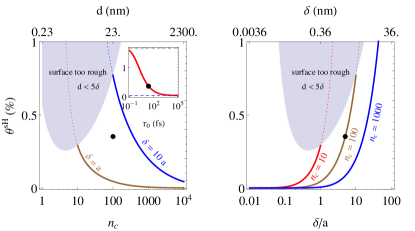
As shown in Fig. 4, the spin Hall angle can be enhanced by i) decreasing film thickness , ii) increasing surface roughness , iii) decreasing bulk relaxation time () or increasing bulk resistivity (). For and , the spin Hall angle for thin films made of Cu, Al, and Ag are listed in Table 1. For Cu, nm and nm, the spin Hall angle for Cu film can reach a fraction of a percent (), which is comparable to that for bulk Au.
Figure 4: (Color online) The spin Hall angle (in percent) for Cu film with the same parameter as in Fig. 2 and . Left: as function of film thickness ; Inset figure shows the dependence on the bulk relaxation time for and with the dashed lines given by the limitting values in Eq. (9); Right: as function of the surface roughness . The black dot in all plots corresponds to the same point with ( nm), nm, fs for Cu with conductivity S/m, and has spin Hall angel .
For comparison, we also carry out the same calculation for a thin film where the spin orbit interaction comes from the impurity scattering instead of the surface scattering, i.e. the in Eq. (2) is replaced by with the spin-orbit interaction parameter for impurity scattering potential .
Following Takahashi et al, Takahashi and Maekawa (2008) we find the coupling parameter of side jump and skew scattering as
(10)
where and is the same conductivity as Eq. (7).
The spin Hall conductivity .
Therefore the spin Hall angle for the bulk impurity induced spin Hall effect in metallic thin film is . Since side jump contribution is a constant, independent of film thickness and/or surface roughness, and skew scattering contribution has the same parameter dependence as the longitudinal conductivity , therefore the spin Hall angle by impurity scattering in metallic thin films decreases with decreasing film thickness and/or increasing surface roughness (following the same trend as in Fig. 2). This behavior is opposite to that for the spin Hall angle by surface scattering (see Fig. 4). Therefore, it is possible to distinguish the origin of the spin Hall effect from the thickness and/or surface roughness dependence of the spin Hall angle.
Material
(S/m)
(1/Å)
Cu
Ag
Au
Al
Table 1: Surface roughness induced spin Hall angle for thin films of several normal metals that has no bulk spin Hall effect. In all cases, , , , and electron effective mass equals to the free electron mass . Data for from Ashcroft and Mermin (1985); Kittel (2005)
To realize the surface roughness induced spin Hall effect experimentally, it is necessary to have two crucial ingredients simultaneously: i) the surface roughness, which acts as surface impurities, ii) the strong interfacial (not bulk) spin-orbit interaction. The former can be controlled by thin film growing process or the surface polishing technique. The latter is possible by coating the metallic thin film surface with materials with large spin orbit interaction, such as Pt or oxides with heavy elements. In such a way, one may utilize the strong scattering due to roughness and the strong spin-orbit interaction from the heavy elements.
In conclusion, we predict that, in metallic thin films without bulk spin-orbit interaction, the spin Hall effect can be realized by surface roughness. For Cu film with sizable interfacial spin-orbit interaction, the spin Hall angle can be as large as a fraction of a percent (), comparable to that in Au.
This work was supported by the special funds for the Major State Basic Research Project of China (2014CB921600, 2011CB925601) and the National Natural Science Foundation of China (91121002).
References
Karplus and Luttinger (1954)
R. Karplus and
J. M. Luttinger,
Phys. Rev. 95,
1154 (1954).
Dyakonov and
Perel (1971a)
M. Dyakonov and
V. Perel,
Physics Letters A 35,
459 (1971a), ISSN
0375-9601.
Dyakonov and
Perel (1971b)
M. I. Dyakonov and
V. I. Perel,
ZhETF Pisma Redaktsiiu 13,
657 (1971b).
Hirsch (1999)
J. E. Hirsch,
Phys. Rev. Lett. 83,
1834 (1999).
Sinova et al. (2004)
J. Sinova,
D. Culcer,
Q. Niu,
N. A. Sinitsyn,
T. Jungwirth,
and A. H.
MacDonald, Phys. Rev. Lett.
92, 126603
(2004).
Kato et al. (2004)
Y. K. Kato,
R. C. Myers,
A. C. Gossard,
and D. D.
Awschalom, Science
306, 1910 (2004),
ISSN 0036-8075, 1095-9203.
Wunderlich et al. (2005)
J. Wunderlich,
B. Kaestner,
J. Sinova, and
T. Jungwirth,
Phys. Rev. Lett. 94,
047204 (2005).
Valenzuela and Tinkham (2006)
S. O. Valenzuela
and M. Tinkham,
Nature 442,
176 (2006), ISSN 0028-0836.
Kimura et al. (2007)
T. Kimura,
Y. Otani,
T. Sato,
S. Takahashi,
and S. Maekawa,
Phys. Rev. Lett. 98,
156601 (2007).
Seki et al. (2008)
T. Seki,
Y. Hasegawa,
S. Mitani,
S. Takahashi,
H. Imamura,
S. Maekawa,
J. Nitta, and
K. Takanashi,
Nat Mater 7,
125 (2008), ISSN 1476-1122.
Takahashi and Maekawa (2008)
S. Takahashi and
S. Maekawa,
Science and Technology of Advanced Materials
9, 014105 (2008),
ISSN 1878-5514.
Saitoh et al. (2006)
E. Saitoh,
M. Ueda,
H. Miyajima, and
G. Tatara,
Appl. Phys. Lett. 88,
182509 (2006).
Murakami et al. (2003)
S. Murakami,
N. Nagaosa, and
S.-C. Zhang,
Science 301,
1348 (2003), ISSN 0036-8075,
1095-9203.
Inoue et al. (2004)
J.-i. Inoue,
G. E. W. Bauer,
and L. W.
Molenkamp, Phys. Rev. B
70, 041303
(2004).
Zhang and Yang (2005)
S. Zhang and
Z. Yang,
Phys. Rev. Lett. 94,
066602 (2005).
Tse and Das Sarma (2006)
W.-K. Tse and
S. Das Sarma,
Phys. Rev. Lett. 96,
056601 (2006).
Krotkov and Das Sarma (2006)
P. L. Krotkov and
S. Das Sarma,
Phys. Rev. B 73,
195307 (2006).
Mott and Massey (1949)
N. F. Mott and
H. S. W. Massey,
The Theory of Atomic Collisions
(Clarendon Press (printed by C. Batey),
1949).
Smit (1958)
J. Smit,
Physica 24, 39
(1958), ISSN 0031-8914.
Berger (1970)
L. Berger,
Phys. Rev. B 2,
4559 (1970).
Nozières and Lewiner (1973)
P. Nozières and
C. Lewiner,
Journal de Physique 34,
901 (1973), ISSN 0302-0738.
Zhang (2000)
S. Zhang,
Phys. Rev. Lett. 85,
393 (2000).
Wang et al. (2013)
X. Wang,
J. Xiao,
A. Manchon, and
S. Maekawa,
Phys. Rev. B 87,
081407 (2013).
Tesanovic et al. (1986)
Z. Tesanovic,
M. V. Jaric, and
S. Maekawa,
Phys. Rev. Lett. 57,
2760 (1986).
Trivedi and Ashcroft (1988)
N. Trivedi and
N. W. Ashcroft,
Phys. Rev. B 38,
12298 (1988).
Ashcroft and Mermin (1985)
N. W. Ashcroft and
N. D. Mermin,
Solid State Physics
(Brooks/Cole, Office,
1985), ISBN 0030839939, 9780030839931.
Kittel (2005)
C. Kittel,
Introduction to solid state physics
(Wiley, 2005), ISBN
047141526X, 9780471415268.