Quantum transport through 3D Dirac materials
Abstract
Bismuth and its alloys provide a paradigm to realize three dimensional materials whose low-energy effective theory is given by Dirac equation in 3+1 dimensions. We study the quantum transport properties of three dimensional Dirac materials within the framework of Landauer-Büttiker formalism. Charge carriers in normal metal satisfying the Schrödinger equation, can be split into four-component with appropriate matching conditions at the boundary with the three dimensional Dirac material (3DDM). We calculate the conductance and the Fano factor of an interface separating 3DDM from a normal metal, as well as the conductance through a slab of 3DDM. Under certain circumstances the 3DDM appears transparent to electrons hitting the 3DDM. We find that electrons hitting the metal-3DDM interface from metallic side can enter 3DDM in a reversed spin state as soon as their angle of incidence deviates from the the direction perpendicular to interface. However the presence of a second interface completely cancels this effect.
keywords:
Three dimensional Dirac material, Bismuth , Landauer-Büttiker formalism , Boundary condition1 Introduction
After discovery of graphene [1], the concept of Dirac fermions became a live and daily-life concept to condensed matter physicists. In the regime of low-energy excitations, the single-particle excitations in graphene obey an effective Hamiltonian that is identical to two dimensional Dirac equation [2]. Some of the intriguing properties inherited from the relativistic-like form of the underlying Dirac equation are, Klein tunneling [3], unconventional Hall effect [4, 5], bipolar super-current [6] and so on. Parallel to the developments in graphene physics, inspired by original proposal of Haldane [7] based on the honeycomb lattice structure of graphene, Kane and Mele constructed a model for two-dimensional topological insulator (TI) [8]. Later on other models of TIs carrying edge modes due to their non-trivial topology were theoretically constructed [9] and experimentally verified [10]. Three dimensional counterparts of the TIs displaying gap in the bulk, and massless Dirac fermions on their surface [11] were all based on the Bismuth element.
The elemental Bismuth was studied since a long time ago and the low-energy effective theory around the L point of Brillouin zone was proposed by Wolf [12] based on two-band approximation of Cohen [13]. It was found that effective theory describing the spin-orbit coupled bands of Bismuth is indeed a three dimensional (3D) massive Dirac theory. Later experiments corroborated the picture of 3D Dirac fermions in this material [14]. More recently, massless 3D Dirac fermions were observed at the point of Brillouin zone of the Na3Bi compound [15]. This provides us with condensed matter realization of both massive and massless Dirac fermions in three spatial dimensions. Therefore it is timely to study the transport properties of 3D Dirac electrons in various settings.
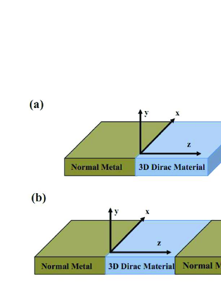
In this paper, we investigate the ballistic transport of 3D Dirac fermions across a boundary separating the 3D Dirac material (3DDM) from the normal metal, as well as the quantum transport through a segment of 3DDM sandwiched between two metallic leads as depicted in Fig. 1. The dynamics of charge carriers inside the 3DDM is described by the 3D Dirac equation, while the electronic states inside the normal metallic leads are governed by the scalar Schrödinger equation. Due to such a difference in the governing equations in the two sides of the interface, the boundary condition matching the electronic states will be tricky and one has to choose the wave-functions so as to give identical current density in both sides of the interfaces separating 3DDM and the normal metals. In the following sections we will formulate this problem and will calculate the transport properties in the ballistic regime within the Landauer-Büttiker formalism.
2 Formulation of the problem
The structure of junctions that we consider in this work is depicted in Fig. 1. In metallic region the carriers obey the Schrödinger equation that means the wave functions is a one-component function; whereas in 3DDM the wave-function describing the charge carrier is an four component spinor satisfying the 3D Dirac equation. An important question is how to construct a boundary condition for matching these two different types of wave-functions across the boundary?
The explicit form of the effective Hamiltonian for the 3DDM is given by [16]:
| (5) |
where is energy gap, is velocity of carriers and denotes the Cartesian components of the wave-vector . The above explicit form corresponds to the following choice of Dirac matrices:
| (10) |
where are Pauli matrices and is unit matrix. The and other matrices are defined as
| (11) |
With the above choice, Hamiltonian can be compactly written as
| (12) |
The ’th component of the current density in 3DDM region is given by
| (13) |
where and the matrices are given by Eq. (11).
The wave-function in the metallic region ( in Fig. 1) satisfies the Schrödinger equation,
| (14) |
with being effective mass of metallic carriers, and is the chemical potential in the normal metallic region with respect to which energy is measured. The current density resulting from the above wave-function is
| (15) |
2.1 The basis in the 3DDM and normal metallic regions
We are going to use the Landauer-Büttiker formulation in order to obtain the transport properties of 3DDM. For this we need to fix a basis with respect to which all the amplitudes will be built.
Let us first discuss the normal metallic region. In this region the one-particle wave-equation is with , where has been introduced to allow for possible difference in the origin of energies in the metallic and 3DMM sides. The wave-function in normal metal is,
| (16) |
where is the wavenumber in normal metal region. and are the amplitudes of right-going and left-going waves, respectively. For this wave function, the current density, Eq. (15) will be given by
| (17) |
To equate this current density to the one arising from solutions of 3D Dirac equation, we need to obtain the expression for the current density in the 3DDM region. With the Hamiltonian in Eq. (5) the wave equation eigen-energies are,
| (18) |
where refers to conduction (valence) band hosting electron (hole) excitations. In Fig.(2), the dispersion relation of Bi is plotted. Each band has a two-fold spin degeneracy. For we have two wave function that corresponds to spin up and down, and are given by,
| (19) |

For case, the wave functions of spin up and spin down hole states are:
| (20) |
When the electrons moving to the right in the normal region reach the interface between the 3DDM and the normal region, the current density of right movers will be given by contributions coming from and spin states. This allows us to write , where () is the contribution of spin () electrons that travel in positive direction inside the normal metal. Corresponding to amplitude of the left-movers in the normal metal, there are amplitudes and of the spin- and spin- left-movers in metallic region satisfying . With this, Eq. (16) in the normal region can be resolved in terms of its and components in the form of
| (21) |
where up to this point the spinorial notation merely indicates that the wave function satisfies two copies of Schödinger equation. At this point following Sepkhanov and coworkers [17], we construct a virtual four-component wave function for metal region as:
| (22) |
The above form has chosen in such a way that when inserted in Eq. (13) that comes from Dirac equation, gives rise to the current given by Eq. (17) that is based on the Schrödinger equation. Therefore we now have a four components wave function which can be used in matching the wave functions at interface. In case of junctions where the velocity in the metallic side and in the 3DDM side are different a pre-factor with must be multiplied to in Eq. (22). Similarly a pre-factor must be multiplied to Eq. (19) to preserve the unitarity of the S-matrix of quantum transport [18]. These pre-factor will cancel the in definition of matrices for 3DDM side and the in the expression for the current density of the normal metallic side. The current density in the normal metal side must be equal to the one in the 3DDM side. With the above point in mind it takes the following form:
| (23) |
This condition will be satisfied when the matching condition at the interface is imposed. This matching condition determines transmission and reflectance coefficients out of which the transport properties can be calculated in standard way. It is important to note that the choice in Eq. (22) for the form of the virtual four-component wave function in the metallic side is not unique. However as long as measurable quantities such as transmission or reflectance are concerned, this choice does not matter and any arbitrary choice will give the same result. Therefore we work with the form given in Eq. (22).
3 Results and Discussion
3.1 Metal-3DDM junction
In this section we consider the transport of positive energy () states corresponding to electron-like particles. The transport of hole-like excitations will be similar. In Fig. 1 (a) we consider an interface separating a metallic region from the 3DDM region. An electron coming from has two possibilities: either passes thorough interface with probability amplitude or reflects to the left with amplitude . Assuming that the incident electron has spin , and putting this in the four-component form, Eq. (22), the wave function in the normal region can be written as,
| (24) |
where () corresponds to reflection coefficient of back scattered electron with spin (). On the other hand the transmitted electron now satisfies the 3D Dirac equation and hence inside the 3DDM region the wave function is of the form,
| (25) |
where () is the transmission amplitude for entering the 3DDM region as an electron with (). Matching the two wave functions in Eq. (24) and Eq. (25) gives the following result for the transmission in the spin and channels, respectively:
| (26) | |||
| (27) |
The above spin-resolved transmission probabilities give the total transmission
| (28) |
It is interesting to note that according to the solutions Eq. (26) and (27), a spin- electron incident from the normal region not only can be transmitted as spin-, but can also be transmitted as spin- electron. The probability amplitude for the later process is given by . This interesting feature is absent for normal incidence where . Therefore electrons hitting the 3DDM at an angle have the chance of being transmitted into 3DDM as spin-flipped. There are also two interesting limiting behavior of the above expressions for the case of normal incidence: (i) In the ” ultra-relativistic” situation where , the total transmission probability always tends to . (ii) When the energy of the incident particle is such that it is injected to the bottom of the positive energy states in the 3DDM, the transmission probability equals .
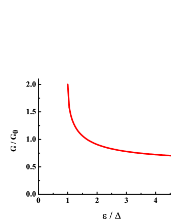
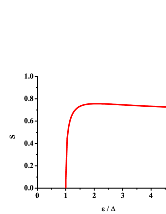
The transmission probability, Eq. (28) can be used to to calculate the conductance and the Fano factor of the junction as,
| (29) |
and
| (30) |
where is the conductance quantum . The Fano factor is the ratio between the current fluctuations and the average current. The counter of the channels in this case in replaced by the wave-vector . Fig. 3 shows the result for the conductance and the Fano factor as a function of the energy in the 3DMM side. As can be seen the behavior is consistend with limiting behavior of transmission coefficients. For we have so that hence per channel, and . In the other limit , and hence per channel and .
3.2 3DDM sandwiched between two metallic regions
In order to experimentally measure the quantum transport through 3DDM, it must be connected to at least two wires from both sides. This corresponds to the situation depicted in Fig. 1-b. In this case there will be two interfaces at and separating the normal metallic region from the 3DDM sandwiched between them. Similar to the case of the interface between a metal and 3DDM, here again we can construct the wave function in the left metal corresponding to spin electron hitting the junction as,
| (31) |
Within the 3DDM region, , we have,
| (32) |
Finally for right metal region we have,
| (33) |
Using the four-component wave-functions for the normal metallic regions along with the the following boundary conditions,
we obtain amazingly simple result for the transmission amplitudes and spin down :
| (34) |
It is interesting to compare the above result with Eq. (27). When an spin electron enters the 3DDM region at a direction not perpendicular to the interface, it always has an amplitude given by Eq. (27) to enter the 3DDM. This is due to the fact that in the 3DDM region the motion of the particle and its spin direction affect each other by strong spin-orbit coupling encoded in the Dirac Hamiltonian. However according to the above equation, when another metallic region is connected to the right of 3DDM, the final electrons reaching the right metallic region can only be in spin state. This can be interpreted as follows: The spin-orbit interaction at each interface allows for spin-flip transmission. However the spin-flip transmission in the two interfaces exactly cancel each other and with two interfaces we only get a net spin-non-flip transmission.
Let us further analyze the transmission through a 3DDM given by Eq. (34). This equation implies that for those modes whose longitudinal wave-vector satisfies , the transmission coefficient is always irrespective of the energy and the transverse component. This is a quite natural generalization of the transmission through graphene that offers two dimensional example of a Dirac material [3].
To discuss another interesting aspect of Eq. (34) let us remember that and where is the incidence angle with respect to the direction normal to the interface. When the 3DDM becomes gap-less, and the propagation direction is normal to the interface, the ratio in Eq. (34) becomes and the transmission amplitude for the incident electron will become,
| (35) |
Therefore carriers hitting the gap-less 3DDM region normal to the interface always pass through it with probability equal to . This is in some sense similar to the Klein paradox. One should however bear in mind that the Klein paradox discusses the tunneling of Dirac electrons form a potential barrier and under normal incidence of massless Dirac fermions one gets a transmission probability equal to . But in the present case we find that massless 3DDM is completely transparent to electrons hitting perpendicularly their interface with a normal metal.
Now let us use the definition of to rewrite Eq. (34) as,
| (36) |
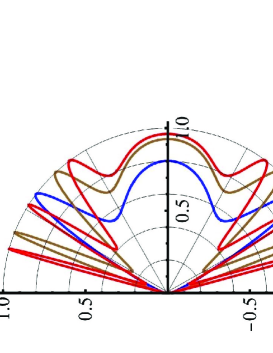
This has been plotted in Fig. 4. Typical value of the energy gap , e.g. in a candidate material such as Bismuth is of order of meV. The typical value of for the same material is about . Therefore when we deal with 3DDM layers with thickness , the effect of energy gap is important. When the 3DDM layer become thinner, the ratio become smaller and therefore the the transport properties will not be sensitive to energy of gap and the system is expected to behave in such a way as if there is no gap.
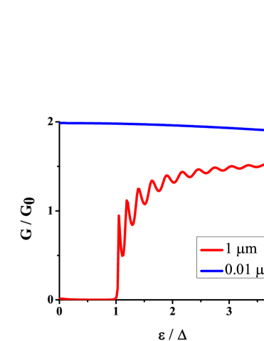
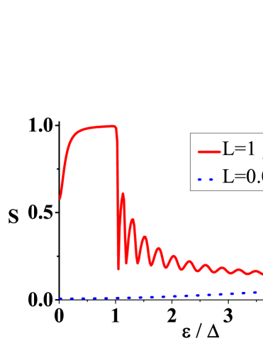
In Fig. 5 we plot the conductance and Fano factor for two different length scales reflecting this point.
When the transverse direction in the and directions confined to lengths and , respectively, the corresponding transverse wave vectors will be quantized. A zero energy electron at hitting the 3DDM from left will not enter the 3DDM as a propagating mode. Hence the current through the 3DDM will be carried as an evanescent mode. The transmission probability in this case becomes [19],
| (37) |
where label the quantized transverse channels. This can be considered as the three dimensional and gapped generalization of a similar result found earlier for graphene [20].
4 Summary and outlook
In this work we studied the transport through a three dimensional Dirac material whose low-energy electronic states are described by massive Dirac Hamiltonian. This theory is specified by a gap parameter and a velocity scale that is usually two or three orders of magnitude smaller than the light velocity. We constructed an artificial four component wave function in the normal metallic region in such a way that the current resulting from this four-component wave function gives precisely the current arising from the corresponding Schrödinger equation. Then the matching condition between a normal metal and the 3DDM can be applied that guarantees
Considering a single interface between a normal metal and a 3DDM we found that electrons hitting the interface at an angle can enter the 3DDM as spin-flipped due to spin-orbit coupling in the 3DDM. For a 3DDM of finite length sandwiched between two normal metallic region we found that the spin-flip transmission at the second interface exactly cancels the one at the opposite interface. We found further that at normal incidence when the gap parameter is zero, the 3DDM becomes completely transparent. This is in some sense similar to the Klein tunneling. We also found that electrons transmitted at the energy corresponding to the bottom of the Dirac conduction band (or holes corresponding to the top of the Dirac valence band) pass through the 3DDM with probability . The 3DDM can also provide transmission through evanescent modes when the incident particle energy corresponds to the mid-gap states of the 3DDM.
5 Acknowledgements
This research was completed while the visit of SAJ to the university of Duisburg supported the Alexander von Humboldt foundation.
References
References
- [1] K. S. Novoselov, A. K. Geim, S. V. Morozov, D. Jiang, M. I. Katsnelson, I. V. Grigorieva, S. V. Dubonos, A. A. Firsov, Two-dimensional gas of massless dirac fermions in graphene, Nature 438 (2005) 197.
- [2] K. S. Novoselov, Nobel lecture: Graphene: Materials in the flatland, Rev. Mod. Phys. 83 (2011) 837–849. doi:10.1103/RevModPhys.83.837.
- [3] M. I. Katsnelson, K. S. Novoselov, A. K. Geim, Chiral tunnelling and the klein paradox in graphene, Nat Phys 2 (9) (2006) 620–625.
- [4] Y. Zhang, Y.-W. Tan, H. L. Stormer, P. Kim, Experimental observation of the quantum hall effect and berry’s phase in graphene, Nature 438 (7065) (2005) 201–204.
- [5] K. S. Novoselov, E. McCann, S. V. Morozov, V. I. Fal/’ko, M. I. Katsnelson, U. Zeitler, D. Jiang, F. Schedin, A. K. Geim, Unconventional quantum hall effect and berry/’s phase of 2[pi] in bilayer graphene, Nat Phys 2 (3) (2006) 177–180.
- [6] H. B. Heersche, P. Jarillo-Herrero, J. B. Oostinga, L. M. K. Vandersypen, A. F. Morpurgo, Bipolar supercurrent in graphene, Nature 446 (7131) (2007) 56–59.
- [7] F. D. M. Haldane, Model for a quantum hall effect without landau levels: Condensed-matter realization of the ”parity anomaly”, Phys. Rev. Lett. 61 (14) (1988) 2015–.
- [8] C. L. Kane, E. J. Mele, Topological order and the quantum spin hall effect, Phys. Rev. Lett. 95 (14) (2005) 146802–.
- [9] B. A. Bernevig, T. L. Hughes, S.-C. Zhang, Quantum spin hall effect and topological phase transition in HgTe quantum wells, Science 314 (5806) (2006) 1757–1761.
- [10] M. König, S. Wiedmann, C. Brüne, A. Roth, H. Buhmann, L. W. Molenkamp, X. Qi, S. C. Zhang, Qntum spin hall insulator state in HgTe quantum wells, Science 318 (5851) (2007) 766–770. doi:10.1126/science.1148047.
- [11] L. Fu, C. L. Kane, E. J. Mele, Topological insulators in three dimensions, Phys. Rev. Lett. 98 (10) (2007) 106803–.
- [12] P. Wolff, Matrix elements and selection rules for the two-band model of bismuth, Journal of Physics and Chemistry of Solids 25 (10) (1964) 1057–1068.
- [13] M. H. Cohen, E. I. Blount, The g-factor and de haas-van alphen effect of electrons in bismuth, Philosophical Magazine 5 (50) (1960) 115–126. doi:10.1080/14786436008243294.
- [14] L. Li, J. G. Checkelsky, Y. S. Hor, C. Uher, A. F. Hebard, R. J. Cava, N. P. Ong, Phase transitions of dirac electrons in bismuth, Science 321 (5888) (2008) 547–550.
- [15] Z. K. Liu, B. Zhou, Y. Zhang, Z. J. Wang, H. M. Weng, D. Prabhakaran, S.-K. Mo, Z. X. Shen, Z. Fang, X. Dai, Z. Hussain, Y. L. Chen, Discovery of a three-dimensional topological dirac semimetal, na3bi, Science 343 (6173) (2014) 864–867.
- [16] Y. Fuseya, M. Ogata, H. Fukuyama, Interband contributions from the magnetic field on hall effects for dirac electrons in bismuth, Phys. Rev. Lett. 102 (6) (2009) 066601–.
- [17] R. A. Sepkhanov, Y. B. Bazaliy, C. W. J. Beenakker, Extremal transmission at the dirac point of a photonic band structure, Phys. Rev. A 75 (6) (2007) 063813–.
- [18] Y. Nazarov, Y. Blanter, Quantum Transport: Introduction to Nanoscience, Cambridge University Press, 2009.
- [19] M. V. Berry, R. J. Mondragon, Neutrino billiards: Time-reversal symmetry-breaking without magnetic fields, Proceedings of the Royal Society of London 412 (1842) (1987) 53–74.
- [20] J. Tworzydło, B. Trauzettel, M. Titov, A. Rycerz, C. W. J. Beenakker, Sub-poissonian shot noise in graphene, Physical Review Letters 96 (24) (2006) 246802.