A statistical study of conductance properties in one-dimensional quantum wires, focusing on the 0.7 anomaly
Abstract
The properties of conductance in one-dimensional (1D) quantum wires are statistically investigated using an array of 256 lithographically-identical split gates, fabricated on a GaAs/AlGaAs heterostructure. All the split gates are measured during a single cooldown under the same conditions. Electron many-body effects give rise to an anomalous feature in the conductance of a one-dimensional quantum wire, known as the ‘0.7 structure’ (or ‘0.7 anomaly’). To handle the large data set, a method of automatically estimating the conductance value of the 0.7 structure is developed. Large differences are observed in the strength and value of the 0.7 structure [from to ], despite the constant temperature and identical device design. Variations in the 1D potential profile are quantified by estimating the curvature of the barrier in the direction of electron transport, following a saddle-point model. The 0.7 structure appears to be highly sensitive to the specific confining potential within individual devices.
I Introduction
One-dimensional (1D) quantum wires can be defined in a two-dimensional electron gas (2DEG) using split-gate nanostructure devices Thornton1986 . The conductance of a quantum wire displays plateaus as a function of gate voltage, quantized in units of the conductance quantum Wharam1988 ; vanWees1988 , which can be understood within a non-interacting framework. However, an anomalous feature appears near –the ‘0.7 structure’ or ‘0.7 anomaly’ Thomas1996 ; Micolich2011 –which occurs as a direct result of electron-electron interactions. This intriguing conductance anomaly continues to inspire efforts to explain its occurrence Bauer2013 ; Iqbal2013 . Many theories have been proposed, including spontaneous spin polarization Thomas1996 ; Wang1996 , quasi-bound state formation and associated Kondo effect Cronenwett2002 ; Meir2002 ; Rejec2006 ; Iqbal2013 , and enhanced electron interactions as electrons slow on passing through the 1D channel, due to the potential barrier Sloggett2008 ; Bauer2013 ; Lunde2009 .
The conductance value of the 0.7 structure () can vary between and Thomas1998 ; Thomas2000 ; Nuttinck2000 ; Wirtz2002 ; Reilly2001 ; Chiatti2006 ; Lee2006 ; Pyshkin2000 ; Hashimoto2001 , and depends on temperature (), magnetic field (), carrier density in the 1D channel, and device geometry. The and dependence of the 0.7 structure are well established Thomas1996 . However, differing results have been reported regarding the dependence on density (summarized in Ref. Burke2012 ) and upon the length of the 1D channel Iqbal2013 ; Reilly2001 . These data were obtained from a variety of 1D devices and confining potentials. This highlights the important role that the confining potential plays in determining Reilly2005 .
Due to limited resources available, many previous experimental studies reproduce results on a handful of devices at most. This prevents statistically significant statements being formulated, and possibly leads to trends being overlooked. Here, a statistical study of the 0.7 structure is presented, using an array of 256 individual split gates with the same dimensions. Experiments were performed during a single cooldown, where each split gate was measured separately by means of a multiplexing scheme described in Ref. Al-Taie2013 . Despite the identical device design, fabrication and measurement conditions, large differences exist in the appearance and value of the 0.7 anomaly. Systematic methods are employed to estimate and the curvature of the potential barrier in the transport direction. The value of appears to be highly sensitive to the specifics of the 1D potential, which differs between even nominally identical split gates.
The outline of the article is as follows. First, the methods of fabricating and measuring the sample are described in Sec. II. We then introduce the properties of the 1D conductance data in Sec. III, highlighting variations which may be related to local fluctuations in the density, thus characterizing the homogeneity of the wafer. Next, we investigate the 0.7 anomaly and its dependence on properties of 1D conductance in Sec. IV. The method of estimating is described, to systematically analyze the large data set. Since the 0.7 anomaly appears exceedingly sensitive to the 1D potential profile, variations in the potential are quantified by developing a model in Sec. V to estimate the curvature of the barrier in the transport direction, through fitting the data with the transmission probability from a saddle-point model. Finally, in Sec. VI we acknowledge the role of disorder in giving rise to other anomalous features in conductance at unexpected values, close to .
II Methods
The sample was fabricated on a modulation-doped GaAs/AlGaAs high electron mobility transistor (HEMT), in which the 2DEG is formed nm below the wafer surface. The 2D carrier density () and mobility () of the 2DEG were measured to be cm-2 and cm2V-1s-1, respectively. The split gates were arranged in a rectangular array, with pitch lengths of 100 and 130 m in the two perpendicular directions. Each split gate was nm long and nm wide, defined using electron-beam (e-beam) lithography [a schematic diagram of a split gate is shown in the inset of Fig. 1(a)]. Two-terminal measurements were performed at K, using an ac excitation voltage of 100 V at Hz. Fifteen split gates failed to define a 1D channel, due to damage to one or both arms of the split gate, which is likely to have occurred during fabrication.
III Properties of 1D conductance
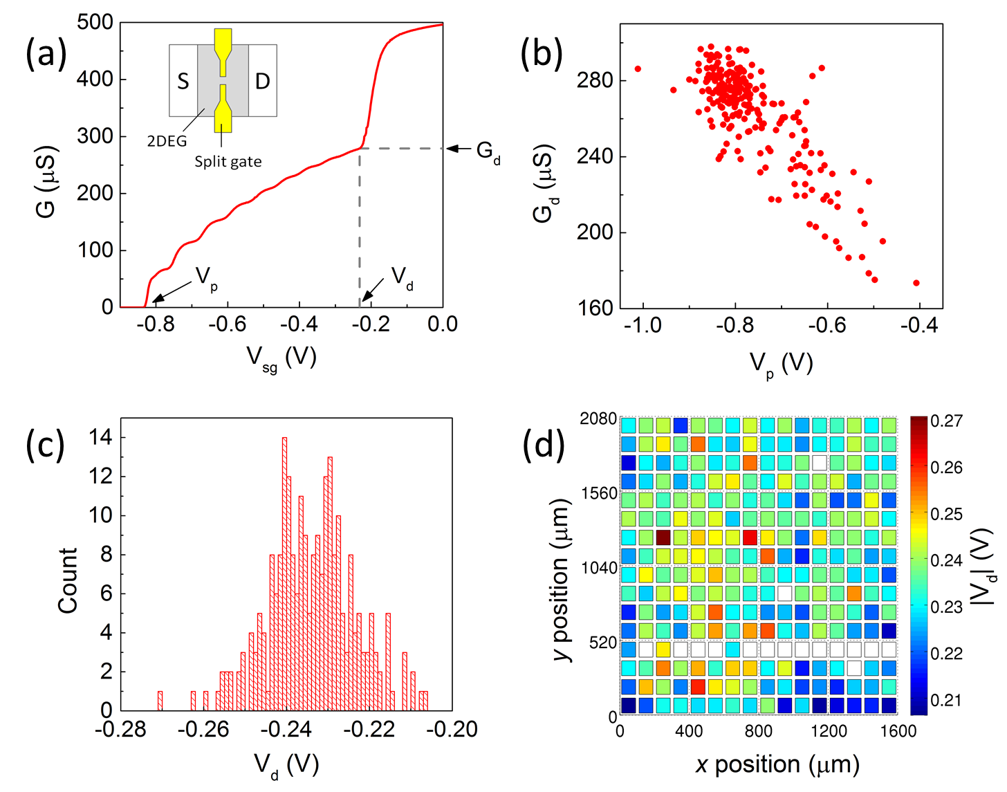
Figure 1(a) shows a typical conductance trace as a function of the voltage applied to the split gate (). Conductance is plotted from to pinch off voltage . There is an initial drop in before a quasi-1D channel forms at (the 1D definition voltage). This is marked by a sudden change in gradient of as a function of . The definition conductance (), and are indicated by arrows in Fig. 1(a).
Figure 1(b) shows a scatter plot of against for 240 devices (241 were measured, however, the conductance of one dropped to zero without defining a 1D channel). The degree of correlation can be quantified using the Pearson product-moment correlation coefficient (), where () corresponds to a perfect positive (negative) correlation, and corresponds to no correlation. There is a strong negative correlation between and in Fig. 1(b), for which . Since in these devices is determined by the number of 1D subbands, a higher suggests that there are more 1D subbands in the channel. The subband spacing may therefore be smaller, requiring the channel to be wider on definition. A stronger electric field (more negative voltage) will be required to fully deplete a wider channel, as reflected in Fig. 1(b). No correlations were apparent between and (), or and ().
Figure 1(c) shows a histogram of , for a bin size of 1 mV. The mean V and standard deviation mV, corresponding to of the mean. Variations in density across the array of split gates may be estimated using from each device (since is the voltage at which the 2D region beneath the gates is depleted). By considering the capacitance between the split gate and the 2DEG, is related to by
| (1) |
where is the electronic charge, is the depth of the 2DEG, and is the dielectric constant of the material. This equation is valid for gate width ; here nm and nm. For V, Eg. (1) gives cm-2 (using for AlGaAs), and cm-2. For comparison, conventional Hall bar measurements on two nearby sections of wafer yielded cm-2 and cm-2.
In this approximation, the capacitance due to the finite density of states in the 2DEG is ignored, since it is small with respect to the geometric capacitance. If it is assumed that changes in density are the only reason for differences in , the distribution of is directly proportional to fluctuations in (i.e. standard deviation corresponds to the same variation in ).
Figure 1(d) shows a color scale (color online) of as a function of the position of each device in the array. On the chip, split gates are separated by 100 and 130 m in the horizontal and vertical directions, respectively, whereas boxes are equally spaced in Fig. 1(d) for convenience. Clear boxes indicate split gates for which could not be determined. Plotting as a function of spatial location illustrates how density fluctuations in a HEMT structure can be investigated on a micron scale. This technique approximately characterizes the homogeneity of a wafer, since variations on this length scale not shown by conventional Hall bar measurements.
IV 0.7 structure
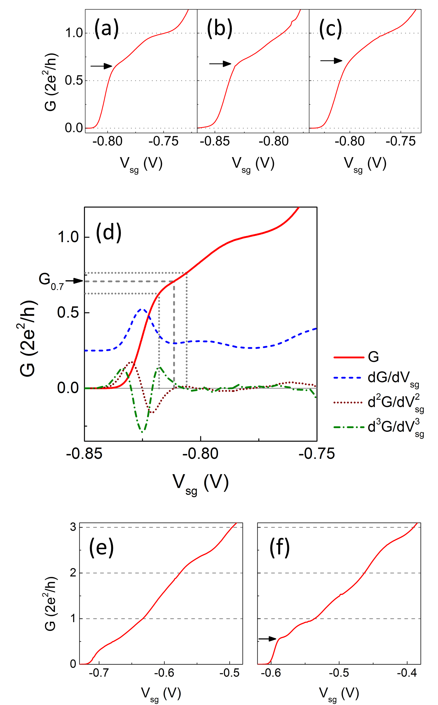
The conductance data from the array of split gates display a large variation in the appearance of the 0.7 structure. Figures 2(a)-(c) show as a function of for three example devices, corrected for series resistance (to ensure consistency, at ). In Figs. 2(a) and 2(b), well-defined structures occur near , marked by the arrows. The feature in Fig. 2(b) is particularly pronounced. A much weaker, shoulder-like structure is shown in Fig. 2(c), indicated by the arrow.
IV.1 Method of estimating
A systematic method of estimating is required to further analyze the data. There is no stated definition of the conductance value that should be assigned to the 0.7 structure note3 ; however, it was the location of the flattest part of the feature–most often observed near –which led to it being given its particular name Thomas2014 . Therefore we present data where is defined as the local minimum in .
Figure 2(d) shows as a function of (solid line) for another example device. The first, second and third derivatives , , and are shown by the dashed, dotted, and dash-dotted curves, respectively. The trace is offset vertically for clarity. The at which (corresponding to the local minimum in ), is shown by the dashed vertical line. This gives our estimate of (indicated by the arrow). The ‘width’ of the 0.7 plateau is estimated as between the closest maximum in to the left and closest maximum in to the right of (indicated by the vertical dotted lines). This defines the bounds of our estimate of , shown by the horizontal dotted lines noteG07bounds .
The value of can be obtained for a limited number of devices using this method, due to variations in shape of the 0.7 structure. If the anomaly is not sufficiently pronounced–for example in Fig. 2(c)– cannot be estimated (since there is no clear minimum in ). However, the resulting benefit is that the data set is reduced to devices for which the conductance characteristics are very similar. Since the strength of the 0.7 structure is related to the relative energy scales within the 1D system, these should therefore be similar for the data remaining.
In addition, we were careful to discard data which showed evidence of disorder at low (below ), since this may affect . Various disorder effects were observed. In some instances the quantization of was significantly affected and no 0.7 structure existed [shown in Fig. 2(e)]. In other cases, a 0.7 structure was observed in addition to disorder effects (these effects included missing or weakened plateaus, deviations in plateau values from multiples of , unusually weak quantization, and resonant features ranging from Coulomb blockade Liang1997 to phase-coherent resonances Kirczenow1989 ). Figure 2(f) shows as a function of for a device in which the second and third plateaus occur below the expected values, and the second plateau is weak. The arrow indicates a strong 0.7 structure. Such data were discarded because we cannot rule out disorder affecting .
After discarding data which showed evidence of disorder, data from 98 split gates remained ( of the 241 measured). An estimate of is obtained for 36 of these 98 devices 07note . This highlights a key benefit of our multiplexing technique: By measuring many devices, we can discard of the data and still retain a data set sufficient for statistical analysis (36 is currently the largest number of devices for which has been estimated from measurements in a single cooldown). We expect a lower rejection ratio for a sample fabricated on a wafer with higher mobility.
While we have have attempted to remove the effect of disorder, thermal broadening of energy levels may mask other disorder effects ( K). Measurements were performed at this in order to observe a well-defined 0.7 anomaly, since we anticipate any statistical (anti)correlation between and other parameters to be most clear at for which the 0.7 anomaly is strongest.
IV.2 Dependence of on properties of 1D conductance
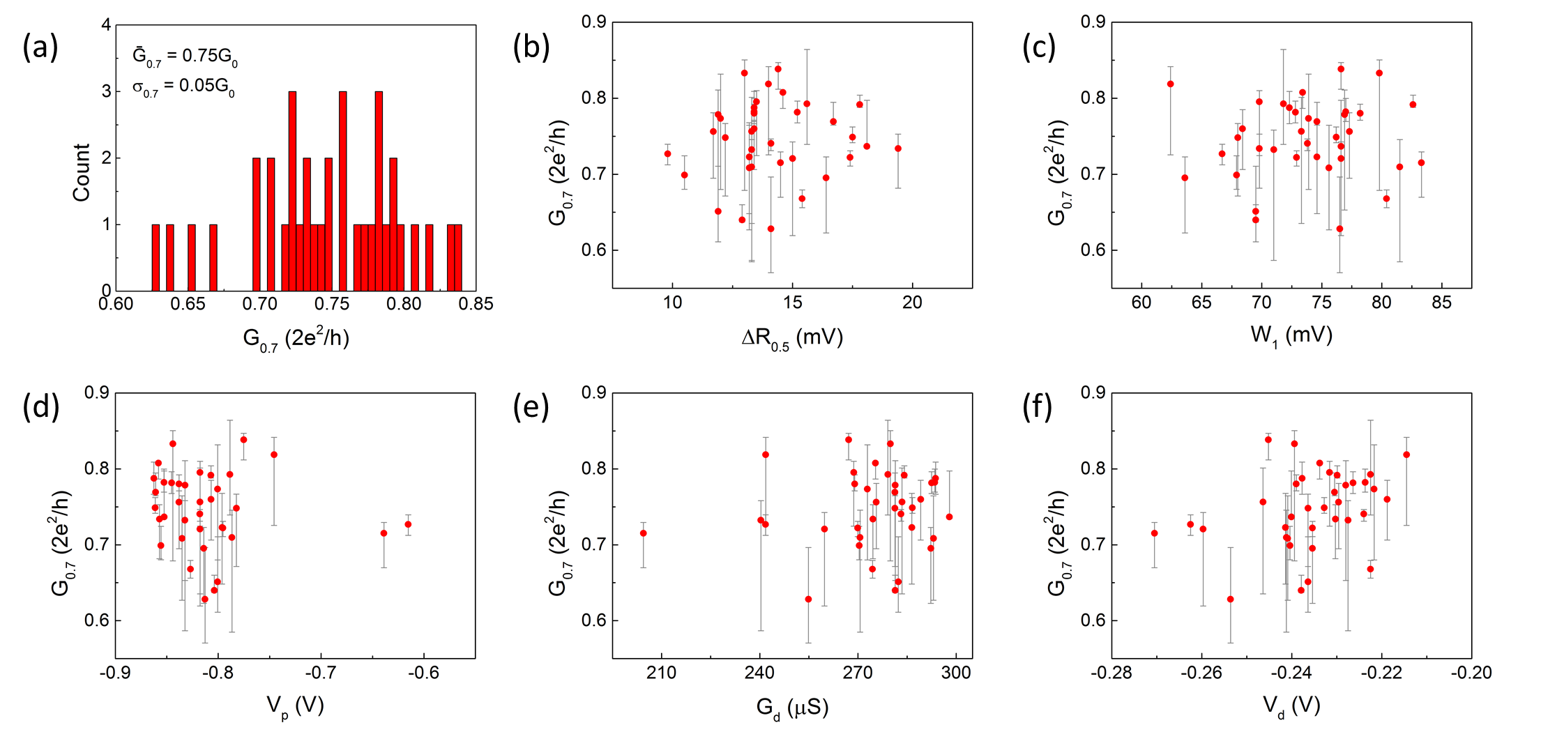
Figure 3(a) shows a histogram of the counts of (for a bin size of ), in which ranges from to . The mean , and standard deviation . The spread of is within that which has been reported previously Burke2012 . However, Fig. 3(a) represents data from devices with a geometrically identical design, which have undergone exactly the same fabrication process, and were measured during a single cooldown at a constant . Therefore the difference of more than in is quite remarkable.
Even though each split gate is patterned with a geometrically-identical design, the shape of the 1D potential profile may vary from device to device. This occurs for a number of reasons including fluctuations in (standard deviation of is estimated to be of the mean, Sec. III), and/or the existence of impurities close to the 1D channel. The differences in suggest it is highly dependent on the shape of the potential profile, and minor variations thereof.
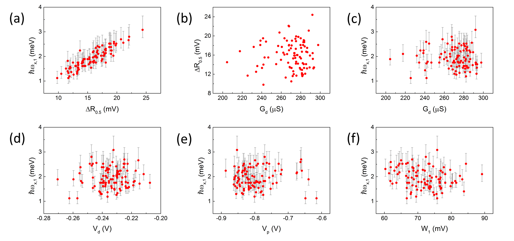
In Figs. 3(b) to (f), is plotted against various properties of the 1D conductance trace. Specifically, Figs. 3(b), (c), (d), (e), and (f) show against , , , , and , respectively, where from to (corresponding to the steepness of the initial rise in towards the 0.7 anomaly), and between and (estimating the width of the first conductance plateau).
These properties of the 1D conductance trace are determined by or reflect physical conditions of the system. For example, indicates the strength of the electrostatic field at pinch off; this field is weaker for values of closer to zero, such that the confinement potential is generally shallower. Lower electron densities also often result in closer to zero. As discussed in Sec. III, and depend on the initial number of 1D subbands in the 1D channel, and fluctuations in , respectively. Additionally, the length of the conductance plateaus depends on the 1D subband spacing, and steepness of the transitions between plateaus depends on the length of the potential barrier in the transport direction (discussed in Sec. V).
A relationship between and any of these properties may illuminate physical conditions which govern . However, no correlations are apparent in Figs. 3(b)-(f); [, , , and , for 3(b), 3(c), 3(d), 3(e), and 3(f), respectively]. Correlations are perhaps hidden because although the properties of conductance may be primarily related to a particular parameter, they are also subject to other influences. These data illustrate that is governed by a combination of conditions and is highly sensitive to the specific potential profile within each device.
V Quantifying the 1D confining potential
To quantify the conditions of confinement within each device one can measure the subband spacing using dc bias spectroscopy Patel1991 . This type of individual characterization is time consuming, and an automated routine of extracting information from the conductance trace is preferred, because of large data set. We therefore fit the data with a transmission probability based on the saddle-point model Buttiker1990 in order to estimate the harmonic oscillator energy , which describes the curvature of the potential barrier in the transport direction.
V.1 Model
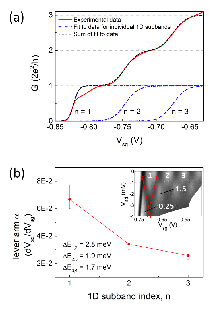
Figure 4(a) shows as a function of (solid line) for an example device. The dashed line shows a fit to the data for the transmission probability , where is the 1D subband index, , is the potential at the center of the 1D channel, and is the energy of the bottom of the 1D subband (relative to ). We deviate from a strict saddle-point model which assumes 1D subbands are equally spaced, since this is not the case for real devices. Additionally, we use a subband-dependent to achieve a better fit to the data.
The conductance is calculated independently for , , and using
| (2) |
where is the Fermi-Dirac distribution . The conductance increases by when chemical potential rises above the bottom of the 1D subband. We choose a reference frame in which each subband edge is initially at , i.e., and . The integration is performed between limits , for K.
The for each subband is then individually scaled by , where is a lever arm relating and obtained from dc bias spectroscopy measurements. We follow the method of estimating described in the supplementary material of Ref. Srinivasan2013 ; , and . Figure 4(b) shows the average values of for each subband from dc bias measurements on four split gates. The error bars are the maximum and minimum estimates of . A grayscale diagram of transconductance as a function of and from one of the devices is shown as an inset to Fig. 4(b). The dark (white) regions correspond to high (low) transconductance, and conductance values of low transconductance regions are labeled in units of . The data are corrected for series resistance (also following the method described in the supplementary material of Ref. Srinivasan2013 ).
To automate the fitting routine, for each split gate is scaled by the average . For simplicity, we also use a constant for each subband, although in reality it varies with . We believe the use of an average to be the most significant source of error in estimating .
The 1D subband spacings were also obtained from the dc bias data. The average and meV, for and , respectively. Since this measurement was performed at K, no feature appears near at small dc bias Patel1991 ; Kristensen2000 . Therefore, was estimated as the crossing point of the tranconductance peaks separating the and regions, and the and regions. This is illustrated by the dashed lines on the grayscale [inset, Fig. 4(b)].
After scaling, the points at which are aligned with the corresponding points on the experimental data, i.e., 0.5, 1.5, and for subbands , and , respectively. A fitting routine is used to find the minimum difference squared between the experimental and calculated conductances. For () the fit was performed between () and (), with fitting parameter (). For , the fit was performed on the lower half of the riser to the first plateau (from to ), to avoid the 0.7 structure.
Figure 4(a) shows after the fitting has been performed, where dot-dashed lines show for individual subbands. The dashed line shows the sum of these data, which overlays the measured (solid line) well. The only fitting parameters used in the model are for , , and . Since this is a non interacting model, there is no 0.7 structure in the fit to the conductance data.
V.2 Dependence of on properties of 1D conductance
Using the method described above, is estimated for the 98 split gates which did not show evidence of disorder below . The mean , and meV, for which the standard deviations , and meV (corresponding to , and of the mean, respectively). This highlights the differences that exist in 1D potential from device to device, despite the lithographically identical design.
The steepness of the initial rise in towards the 0.7 anomaly is given by from to . Figure 5(a) shows a scatter plot of against . This is a helpful check of the quality of the fit, since the fitting was performed over this range of . There is a strong degree of correlation (Pearson product-moment correlation ). Thus, the steepness of the transition to for the fitted accurately reflects that of measured data, indicating that the fit is reasonable. Error bounds are given by finding for the upper and lower values of shown in Fig. 4(b).
Figure 5(b) shows against the 1D definition conductance . While there is no apparent correlation, there seems to be relatively distinct diagonal cutoff above which there are no data points (in the top-left triangular section of the plot). Thus, a sharper initial rise in conductance tends to correspond to a lower . In Fig. 5(c), is plotted against . The diagonal cutoff is reflected here, although less distinctly.
Figures 5(d), 5(e), and 5(f) show against , , and , respectively. No correlations are apparent between and these other properties of the 1D conductance trace (no correlations were also evident between or and these properties). It is possible that trends may be masked by errors in the lever arm . However, the spread in for most values of , , and is larger than the estimated error.
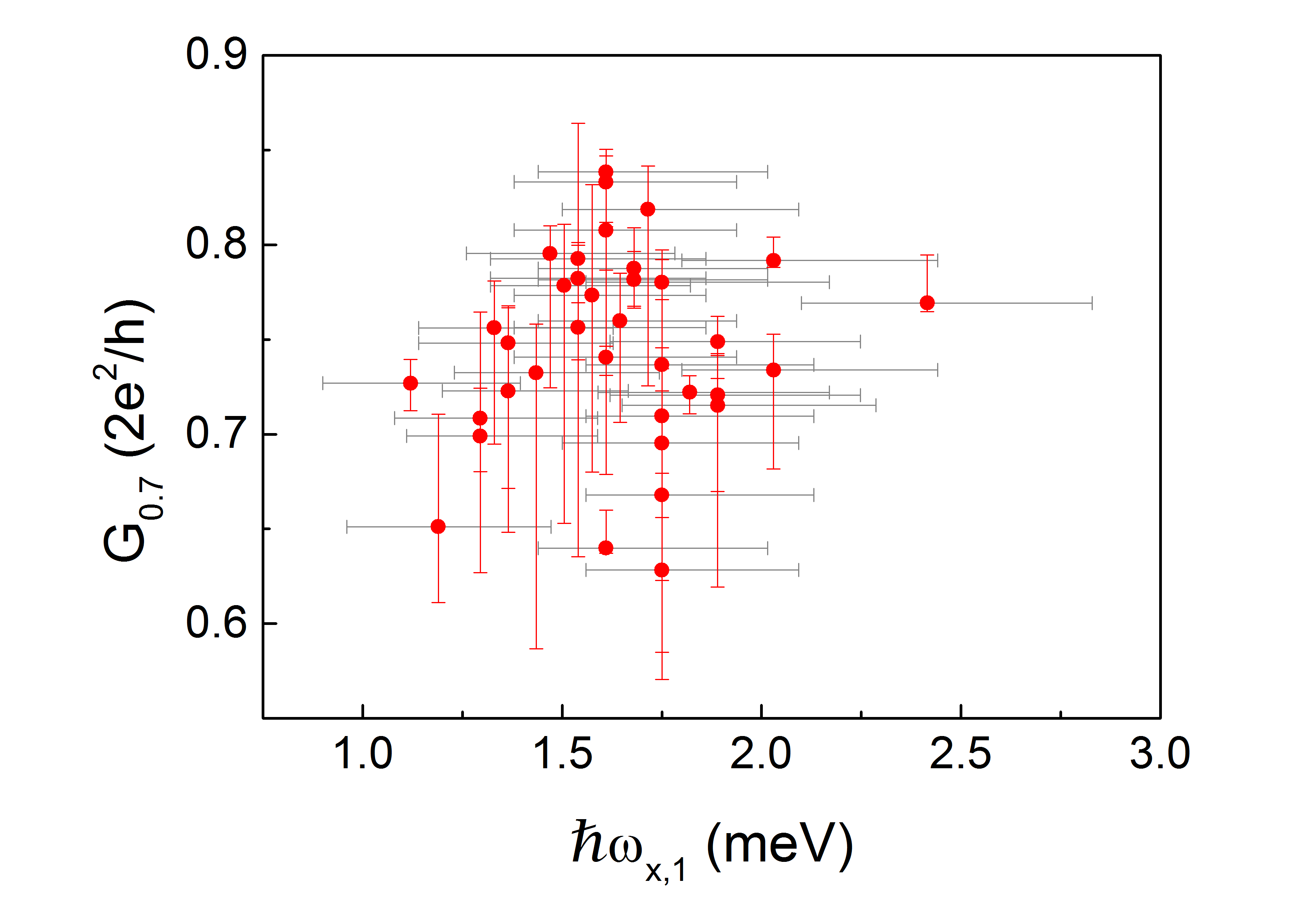
V.3 Dependence of on
Figure 6 shows a scatter plot of against . For these data , indicating an exceedingly weak correlation. Unfortunately, any correlation which may exist is likely to be masked by errors in the estimate of . We believe the error in to be less significant since is given by a well-defined point (the local minimum in ), and bounds in are instead related to the width of the conductance anomaly noteG07bounds . The error in could be reduced by using the correct for each device. This requires dc bias measurements to be performed for every device.
A specific correlation between and is predicted by certain models for the origin of the 0.7 structure. For example, the 1D Kondo effect occurs when electrons are localized within a 1D channel Sfigakis2008 . In the 1D Kondo scenario, for large the Kondo temperature () is also high Meir2002 ; Rejec2006 ; Hirose2003 . Thus, an increase in () should cause to increase at a given temperature, since . However, other models expect the opposite trend. It has been proposed that the 0.7 structure is related to enhanced interactions as the electrons slow down on passing through the 1D barrier Sloggett2008 ; Bauer2013 ; Lunde2009 . Of these models, only one Sloggett2008 studies the high-temperature dependence of with . If the 1D barrier is a saddle-point potential Buttiker1990 , the value of is predicted to decrease as increases. We do not observe a strong enough trend in our data to support one theory above another.
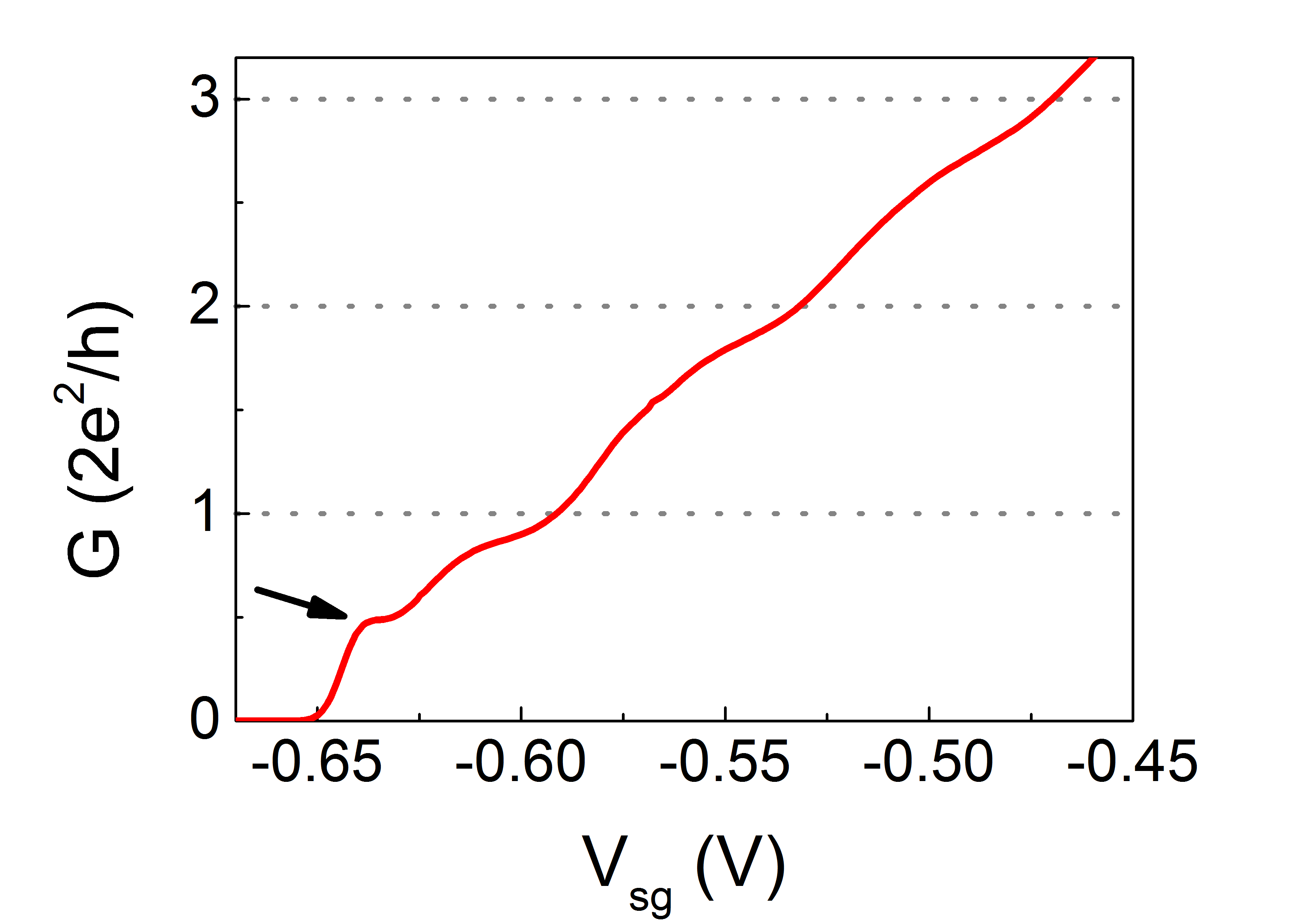
VI Anomalous conductance features near
Conductance anomalies were also observed at values lower than the range shown in Fig 3(a). Figure 7 shows as a function of for a device in which an anomalous feature occurs at (marked by the arrow). Of the 241 split gates measured, showed conductance anomalies at this value; it is therefore unusual to find features at in 1D devices on GaAs/AlGaAs heterostructures for T (the magnetic field at which these measurements were performed). These data were not included in the analysis because of evidence of disorder; for example, in Fig. 7 the plateaus do not appear at correct values SeriesRes . The co-existence of disorder effects may be responsible for the lowering of the conductance of the 0.7 structure to .
A statistical measurement makes it possible to distinguish the “normal” characteristics from device-specific effects, which may be related to disorder. Devices which display unusual conductance anomaly can be investigated for rare physical phenomena, while very clean devices can be used to identify standard behavior.
The reproducibility of conductance characteristics has been investigated by thermally cycling the sample. It was found that many of the split gates which showed evidence of disorder did so on both cooldowns Al-Taie2013B . The aim of the current article is to compare properties of 1D conductance from a large number of devices on a single cooldown. The reproducibility of these properties on thermal cycling warrants a further, separate study.
The sample was also illuminated with a light-emitting diode (LED), which increased and to cm-2 and cm2V-1s-1, respectively. This resulted in longer, better-defined plateaus in conductance, since the 1D confining potential becomes stronger and the 1D subband spacing increases. However, many devices showed occasional structure in conductance which had the appearance of resonant transmission through the quantum wire, consistent with an enhancement of resonant effects due to sharper confinement Kirczenow1989 . We did not investigate or in this case since the estimates are very likely to be affected by the resonances.
VII Conclusion
Across an array of nominally identical split gates (measured at a single ), significant fluctuations were seen to exist in the 1D potential. These have been quantified by estimating the curvature of barrier in the transport direction () for each device. Large variations were observed in both the appearance of the 0.7 structure and the value at which it occurred. The 0.7 structure appears to be extremely sensitive to the specific 1D potential in each device. Measuring many devices has enabled a statistical study to be performed. No correlations were apparent between and , or other properties of the 1D conductance trace.
A specific set of physical conditions combine to give a particular conductance trace for a split gate. With the current analysis, the effect of individual factors influencing the conductance properties cannot be separated. Thus, parameters which may govern and have not been identified. This may become possible by performing dc bias spectroscopy for each device in order to accurately measure 1D subband spacing and lever arm , thereby giving a better estimate of .
The confining potential will be affected by fluctuations in the background potential due to the ionized dopants (leading to local density variations) and the existence of impurities (giving rise to disorder effects). We removed data which showed evidence of disorder from the analysis, although a fuller study requires - and -dependent measurements (since disorder effects will be masked at the temperature at which the measurements were performed). We have shown that disorder does give rise to conductance anomaly at unexpected values, e.g., close to . Disorder effects can be reduced by fabricating samples on a wafer with higher electron mobility, or using an undoped heterostructure and electrostatically inducing the 2DEG See2012 ; Harrell1999 ; Sarkozy2009 .
This work was supported by the Engineering and Physical Sciences Research Council Grant No. EP/I014268/1. The authors thank T.-M. Chen, C. J. B. Ford, I. Farrer, E. T. Owen and K. J. Thomas for useful discussions, and R. D. Hall for e-beam exposure.
Corresponding author. E-mail address: lws22@cam.ac.uk
References
- (1) T. J. Thornton, M. Pepper, H. Ahmed, D. Andrews, and G. J. Davies, Phys. Rev. Lett. 56, 1198 (1986).
- (2) B. J. van Wees, H. van Houten, C. W. J. Beenakker, J. G. Williamson, L. P. Kouwenhoven, D. van der Marel, and C. T. Foxon, Phys. Rev. Lett. 60, 848 (1988).
- (3) D. A. Wharam, T. J. Thornton, R. Newbury, M. Pepper, J. Ahmed, J. E. F. Frost, D. G. Hasko, D. A. Ritchie, and G. A. C. Jones, J. Phys. C 21, L209 (1988).
- (4) K. J. Thomas, J. T. Nicholls, M. Y. Simmons, M. Pepper, D. R. Mace, and D. A. Ritchie, Phys. Rev. Lett. 77, 135 (1996).
- (5) A. P. Micolich, J. Phys. Condens. Matter 23, 443201 (2011).
- (6) F. Bauer, J. Heyder, E. Schubert, D. Borowsky, D. Taubert, B. Bruognolo, D. Schuh, W. Wegscheider, J. von Delft, and S. Ludwig, Nature (London) 501, 73 (2013).
- (7) M. J. Iqbal, R. Levy, E. J. Koop, J. B. Dekker, J. P. de Jong, J. H. M. van der Velde, D. Reuter, A. D. Wieck, R. Aguado, Y. Meir and C. H. van der Wal, Nature (London) 501, 79 (2013).
- (8) C.-K. Wang and K.-F. Berggren, Phys. Rev. B 54, R14257 (1996).
- (9) S. M. Cronenwett, H. J. Lynch, D. Goldhaber-Gordon, L. P. Kouwenhoven, C. M. Marcus, K. Hirose, N. S. Wingreen, and V. Umansky, Phys. Rev. Lett. 88, 226805 (2002).
- (10) Y. Meir, K. Hirose, and N. S. Wingreen, Phys. Rev. Lett. 89, 196802 (2002).
- (11) T. Rejec and Y. Meir, Nature (London) 442, 900 (2006).
- (12) C. Sloggett, A. I. Milstein, and O. P. Sushkov, Eur. Phys. J. B 61, 427432 (2008).
- (13) A. M. Lunde, A. De Martino, A. Schulz, R. Egger, and K. Flensberg, New Journal of Physics 11, 023031 (2009).
- (14) K. J. Thomas, J. T. Nicholls, N. J. Appleyard, M. Y. Simmons, M. Pepper, D. R. Mace, W. R. Tribe, and D. A. Ritchie, Phys. Rev. B 58, 4846 (1998).
- (15) K. J. Thomas, J. T. Nicholls, M. Pepper, W. R. Tribe, M. Y. Simmons, and D. A. Ritchie, Phys. Rev. B 61 13365 (2000).
- (16) S. Nuttinck, K. Hashimoto, S. Miyashita, T. Saku, Y. Yamamoto, and Y. Hirayama, Jpn. J. Appl. Phys. 39, L655 (2000).
- (17) R. Wirtz, R. Newbury, J. T. Nicholls, W. R. Tribe, M. Y. Simmons, and M. Pepper, Phys. Rev. B 65, 233316 (2002).
- (18) K. S. Pyshkin, C. J. B. Ford, R. H. Harrell, M. Pepper, E. H. Linfield, and D. A. Ritchie, Phys. Rev. B 62, 15842 (2000).
- (19) K. Hashimoto, S. Miyashita, T. Saku, and Y. Hirayama, Jpn. J. Appl. Phys. 40, 3000 (2001).
- (20) D. J. Reilly, G. R. Facer, A. S. Dzurak, B. E. Kane, R. G. Clark, P. J. Stiles, R. G. Clark, A. R. Hamilton, J. L. O’Brien, N. E. Lumpkin, L. N. Pfeiffer, and K. W. West, Phys. Rev. B 63, 121311 (2001).
- (21) O. Chiatti, J. T. Nicholls, Y. Y. Proskuryakov, N. Lumpkin, I. Farrer, and D. A. Ritchie, Phys. Rev. Lett. 97, 056601 (2006).
- (22) H.-M. Lee, K. Muraki, E. Y. Chang, and Y. Hirayama, J. Appl. Phys. 100, 043701 (2006).
- (23) A. M. Burke, O. Klochan, I. Farrer, D. A. Ritchie, A. R. Hamilton, and A. P. Micolich, Nano Lett. 12, 4495 (2012).
- (24) D. J. Reilly, Phys. Rev. B 72, 033309 (2005).
- (25) H. Al-Taie, L. W. Smith, B. Xu, P. See, J. P. Griffiths, H. E. Beere, G. A. C. Jones, D. A. Ritchie, M. J. Kelly, and C. G. Smith, Appl. Phys. Lett. 102, 243102 (2013).
- (26) There is, however, an operational definition: The apparent anomaly should (1) become stronger with increasing temperature, (2) monotonically lower to with increasing magnetic field, and (3) should not move up or down in conductance when the conducting 1D channel is laterally shifted left or right with asymmetric voltages on the gates.
- (27) K. J. Thomas (private communication).
- (28) The bounds of provide an estimate of the error. However, is given by a well-defined point (the local minimum in ). Also, between the upper and lower bounds is very strongly correlated with between the nearest maximum in and to the 0.7 anomaly. Therefore, the bounds of are perhaps better seen as representing the width of the conductance anomaly.
- (29) C.-T. Liang, I. M. Castleton, J. E. F. Frost, C. H. W. Barnes, C. G. Smith, C. J. B. Ford, D. A. Ritchie, and M. Pepper, Phys. Rev. B 55, 6723 (1997).
- (30) G. Kirczenow, Phys. Rev. B 39, 10452 (1989).
- (31) This is not to say that the 0.7 anomaly did not exist in the remainder of devices, but there was no clear minimum in .
- (32) N. K. Patel, J. T. Nicholls, L. Martín-Moreno, M. Pepper, J. E. F Frost, D. A. Ritchie, and G. A. C. Jones, Phys. Rev. B 44, 13549 (1991).
- (33) M. Büttiker, Phys. Rev. B 41, 7906 (1990).
- (34) A. Srinivasan, L. A. Yeoh, O. Klochan, T. P. Martin, J. C. H. Chen, A. P. Micolich, A. R. Hamilton, D. Reuter, and A. D. Wieck, Nano Lett. 13, 148 (2013).
- (35) A. Kristensen, H. Bruus, A. E. Hansen, J. B. Jensen, P. E. Lindelof, C. J. Marckmann, J. Nygård, C. B. Sørensen, F. Beuscher, A. Forchel, and M. Michel, Phys. Rev. B 62, 10950 (2000).
- (36) F. Sfigakis, C. J. B. Ford, M. Pepper, M. Kataoka, D. A. Ritchie, and M. Y. Simmons, Phys. Rev. Lett. 100, 026807 (2008).
- (37) K. Hirose, Y. Meir, and N. S. Wingreen, Phys. Rev. Lett. 90, 026804 (2003).
- (38) The data are corrected for series resistance using at , such that all split gates in a single row (16 devices Al-Taie2013 ) are corrected using the same value. In most cases this resulted in correctly quantized plateaus. Therefore, the suppression of plateaus (as in Fig. 7) was interpreted as evidence of disorder.
- (39) H. Al-Taie, L. W. Smith, B. Xu, P. See, J. P. Griffiths, H. E. Beere, G. A. C. Jones, D. A. Ritchie, M. J. Kelly, and C. G. Smith, arXiv:1407.5806.
- (40) A. M. See, I. Pilgrim, B. C. Scannell, R. D. Montgomery, O. Klochan, A. M. Burke, M. Aagesen, P. E. Lindelof, I. Farrer, D. A. Ritchie, R. P. Taylor, A. R. Hamilton, and A. P. Micolich, Phys. Rev. Lett. 108, 196807 (2012).
- (41) R. H. Harrell, K. S. Pyshkin, M. Y. Simmons, D. A. Ritchie, C. J. B. Ford, G. A. C. Jones, and M. Pepper, Appl. Phys. Lett. 74, 2328 (1999).
- (42) S. Sarkozy, F. Sfigakis, K. Das Gupta, I. Farrer, D. A. Ritchie, G. A. C. Jones, and M. Pepper, Phys. Rev. B 79, 161307(R) (2009).