Engineering near infrared single photon emitters in ultrapure silicon carbide
Quantum emitters hosted in crystalline lattices are highly attractive candidates for quantum information processing Waldherr:2014kt , secure networks Togan:2010hi ; DeGreve:2012iv and nanosensing Mamin:2013eu ; Staudacher:2013kn . For many of these applications it is necessary to have control over single emitters with long spin coherence times. Such single quantum systems have been realized using quantum dots Atature:2007dk , colour centres in diamond Balasubramanian:2009fu , dopants in nanostructures Siyushev:2014ie and molecules Nothaft:2012eo . More recently, ensemble emitters with spin dephasing times on the order of microseconds Koehl:2011fv ; Soltamov:2012ey and room-temperature optically detectable magnetic resonance Kraus:2013di have been identified in silicon carbide (SiC), a compound being highly compatible to up-to-date semiconductor device technology. So far however, the engineering of such spin centres in SiC on single-emitter level has remained elusive Baranov:2011ib . Here, we demonstrate the control of spin centre density in ultrapure SiC over 8 orders of magnitude, from below to above using neutron irradiation. For a low irradiation dose, a fully photostable, room-temperature, near infrared (NIR) single photon emitter can clearly be isolated, demonstrating no bleaching even after excitation cycles. Based on their spectroscopic fingerprints, these centres are identified as silicon vacancies, which can potentially be used as qubits Riedel:2012jq , spin sensors Kraus:2013vf and maser amplifiers Kraus:2013di .
Silicon vacancy ()-related defects in SiC can significantly exceed the performance of on-chip photonic networks and long-distance quantum communication systems, compared to many other solid-state single photon emitters. In particular, the zero-phonon lines (ZPLs) of -related defects in 4H, 6H and 3C polytypes of SiC present spectrally narrow features at NIR wavelengths . Rayleigh scattering losses in photonic structures are inversely proportional to the fourth power of the wavelength, giving almost one order of magnitude lower losses for these defects compared to the nitrogen-vacancy defect in diamond () Kurtsiefer:2000tk or the carbon antisite-vacancy pair in SiC () Castelletto:2013el . Similarly, scattering losses at interfaces and signal attenuation in optical fibers decrease with wavelength as well. Furthermore, -related defects in SiC can be integrated with existing optoelectronic devices Fuchs:2013dz and, in contrast to GaAs-based quantum dots Yuan:2001dp , operate even at room temperature.
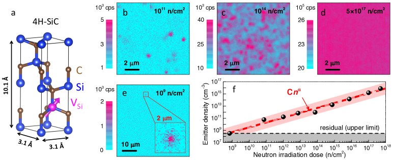
The 4H-SiC unit cell with single defect is shown in Fig. 1(a). The dangling bonds of four C atoms with the absent Si atom result in formation of energy levels within the forbidden gap () of 4H-SiC Bockstedte:2003fn ; Gali:2012jy . In case of negatively-charged , five electrons form a spin quadruplet () in the ground state Mizuochi:2002kl ; Kraus:2013di . To excite these defects we use sub-band gap excitation of SiC at a laser wavelength of (), which is close to their optimal excitation wavelength Hain:2014tl . At room temperature, the defects emit in the NIR spectral range from to . At cryogenic temperatures, two distinct ZPLs at (V1) and (V2), associated with two different crystallographic sites in 4H-SiC, are observed in the photoluminescence (PL) spectrum Sorman:2000ij , which can be used as spectroscopic fingerprints of .
To control the density in a high-quality 110--thick 4H-SiC epitaxial layer Hain:2014tl , we used neutron irradiation () in a fission reactor. The irradiation dose was varied over more than 8 orders of magnitude, from to (Fig. 1). Some part of the generated defects are negatively charged due to the presence of residual N donors (). Additionally, the neutron transmutation doping may play a role.

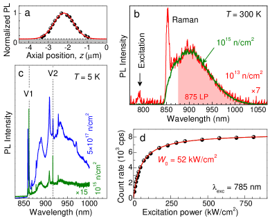
A PL confocal raster scan () on a sample irradiated with a low dose of is presented in Fig. 1(b). The PL is detected in the spectral range from [owing to a longpass (LP) filter] to [limited by the sensitivity of Si avalanche photodiodes (APDs)]. Four, nearly diffraction-limited spots [full width at half maximum (FWHM) of ca. ] are clearly seen in this scan. With rising irradiation dose to the number of PL spots increases as well [Fig. 1(c)]. For the highest irradiation dose of single PL spots cannot be resolved any more and the PL spatial distribution becomes highly homogeneous [Fig. 1(d)]. Remarkably, in the negligibly weak irradiated sample (dose of ) only one PL spot is found in the raster scan [Fig. 1(e)]. The single spots are also restricted along the optical axis as shown in Fig. 2(a). Below we unambiguously prove that these intensity spots are due to the emission from single defects.
In order to find the density of single photon emitters the following procedure is used. Up to the irradiation dose of we directly count the number of PL spots in the detection volume, given by the scanned area and the focus depth, the latter is about according to Fig. 2(a). For this irradiation dose we also measure the integrated PL intensity collected from an area of about . This PL is used as a reference to calculate the emitter density in the strongly irradiated samples by comparing PL intensities. The results are presented in Fig. 1(f). For the lowest irradiation dose the defect density is , which can be taken as the upper limit of residual concentration in our 4H-SiC sample. The concentration after the highest irradiation dose constitutes . The irradiation dose dependence follows quite well a polynomial scaling , as shown by the solid line in Fig. 1(f).

To identify the type of generated defects, we measure the PL spectra for different irradiation doses. The spectrum from a single center is identical to the ensemble emission [Fig. 2(b)]. Here we use a LP filter to suppress the excitation light at in the detection path. The LO phonon Raman line from 4H-SiC at is independent of the irradiation dose and hence is masked by the stronger PL band for . We therefore use an additional LP filter when investigating single centers. The PL spectra recorded at low temperature () are presented in Fig. 2(c). Two characteristic lines at and are clearly visible for different irradiation doses. These lines coincide with the V1 and V2 ZPLs Sorman:2000ij , proving that the PL originates from the defects in 4H-SiC.

As expected for single defect centers, the PL intensity saturates with increasing excitation power density [Fig. 2(d)]. After subtracting the linear background contribution and APD dark counts, it follows
| (1) |
Here, is the saturation power density exposed to the sample, corresponding to the laser power at the objective entrance aperture. The saturation PL intensity varies slightly from spot to spot and in Fig. 3(d) yields counts per second (cps).
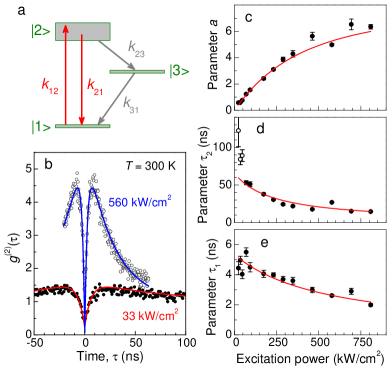
As a next step, we perform the Hanbury-Brown and Twiss (HBT) interferometry experiment, i.e., the time correlation measurement of photon detection by two APDs. This is a frequently used method to verify single photon emission Kurtsiefer:2000tk ; Castelletto:2013el . The second-order correlation functions , recorded over several hours for different , are shown in Fig. 3(b). The most important feature is the dip at zero time delay (). For the lowest excitation, we obtain , which denotes clearly the non-classical behavior of a single photon emitter. Additionally to the anti-bunching for there is also bunching for . In order to explain such a behaviour at least three levels should be involved [Fig. 3(a)].
The second-order correlation function can be well described using
| (2) |
as shown by the solid lines in Fig. 3(b). The power dependencies of parameters , and are presented in Figs. 3(c)-(e), respectively. We use the same three-level model as for the colour centres in diamond Kurtsiefer:2000tk ; Aharonovich:2010bj ; Neu:2011ik to fit these dependencies. This model describes reasonably well the bunching amplitude [the solid line in Fig. 3(c)] and the anti-bunching decay time [the solid line in Fig. 3(e)]. However, the relatively long bunching decay time for is not well reproduced within this model [the solid line in Fig. 3(d)]. The fit for also provides significantly different transition rates as that for and . A possible explanation is that a deshelving process of the metastable state may occur under optical excitation Neu:2011ik .
In order to find the transition rates of the three-level model in Fig. 3(a), we take the limiting values for and as an approximation for . We obtain , , , and the corresponding lifetimes are summarised in table 1. Remarkably, the value for agrees well with the PL decay time of observed in time-resolved experiments Hain:2014tl and remarkably longer than that of the band-to-band transition in semiconductor nanostructures Yakovlev:2000ez . The excitation rate of is proportional to the laser power density , where the absorption cross section can be calculated from the saturation behaviour of Fig. 2(d) as . Here, we take for the transmission coefficient at the SiC surface and the calculated value for is also presented in table 1.

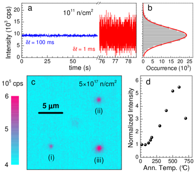
Photostability is an important characteristic of a single photon emitter. The PL time traces of a single defect are shown in Fig. 4(a). For a sampling bin to the count rates remain constant over minutes. In order to examine the photostability on a shorter time scale, the sampling bin is reduced to . The number of detected photons per sampling bin is 10 in this case, and the time trace demonstrates statistical fluctuations without any indication of blinking [Fig. 4(b)]. We have investigated a single emitter over more than one week under continuous excitation and did not observe photobleaching. Assuming that the excitation occurs on average every , this corresponds to excitation cycles.
Finally we found that in the highly irradiated sample the PL intensity increases locally upon laser illumination. To demonstrate this effect, the laser of different intensities was focussed sequently on three different spots and remained there for 120 minutes, respectively. A confocal raster scan, performed at low laser power after such a procedure, demonstrates clearly a PL enhancement for each spot, as shown in Fig. 4(c). For the highest laser power [spot (iii) in Fig. 4(c)] this enhancement is ca. 25%. Remarkably, the generated pattern of Fig. 4(c) preserves at least one day.
Our interpretation is that the focused laser beam locally heats the sample, resulting in atomic displacements and thus in disappearance or/and transformation of some other types of intrinsic defects, generated upon neutron irradiation. These defects may serve as non-radiative recombination channels or as charge traps, switching off the defects in close proximity. In order to corroborate this explanation, we perform complementary annealing experiments by increasing stepwise the temperature and monitoring the PL intensity after each step. The results are summarized in Fig. 4(d), showing the overall PL enhancement by a factor of . This corresponds to and demonstrates that defects can be created at high density in a controlled manner, as required, for instance, for the implementation of a SiC maser Kraus:2013di .
In our experiments, we precisely control the concentration of defects in ultrapure 4H-SiC down to single defect level. This approach can be used to deterministically incorporate these atomic-scale defects in electronic Fuchs:2013dz and photonic structures Calusine:2014gv as well as in nanocrystals. Together with their extremely narrow optical resonances (on the order of at low temperature Riedel:2012jq ) and recently demonstrated optically-detected spin resonances at ambient conditions Kraus:2013vf , our results open exciting opportunities for various quantum applications with spin-photon interface.
Methods
Samples
The 4H-SiC sample has been purchased from CREE. A high purity (residual nitrogen doping below ) layer of thickness was epitaxially grown on a 2-inch n-type 4H-SiC wafer. The layer is covered by a 5--thick n-type 4H-SiC layer and a 2--thick p-type 4H-SiC layer. The wafer was diced in pieces, which were then irradiated in a TRIGA Mark-II nuclear reactor, with neutron energies in the range of MeVMeV.
The sample with the highest neutron irradiation dose of was thermally annealed in several steps from to for a time of 90 minutes, respectively. The heating was either performed on a heat stage (–) or in an oven (–).
Experimental setup
Samples were investigated with a home-build confocal microscope and a cw 785 nm laser was used for excitation. A three dimensional piezo unit (nPoint) was used to move the SiC sample in lateral and axial directions. The excitation beam was focused onto the samples by a high aperture () oil immersion microscope objective (UAPON 100XOTIRF, Olympus). Collimated optical response of the sample was collected by the same objective and guided through a 30 or 75 pinhole (Thorlabs) followed by a 850 and 875 nm LP filter (Edmund Optics). Time correlated single photon counting (TCSPC) was recorded by a HBT setup consisting of two APDs (Count-100C-FC, Laser-components GmbH) with a quantum efficiency of about 0.3 at the signal wavelength and less than 100 cps in the dark and a 16-channel photon correlator card (DPC-230, Becker&Hickl GmbH) with a time resolution of at least 165 ps.
The low temperature PL spectra were measured at 5 K in a cryostat (MicrostatHe, Oxford Instruments) built into a confocal Raman spectrometer (LabRAM HR, Horiba). The excitation wavelength was 633 nm.
References
- (1) Waldherr, G. et al. Quantum error correction in a solid-state hybrid spin register. Nature 506, 204–207 (2014).
- (2) Togan, E. et al. Quantum entanglement between an optical photon and a solid-state spin qubit. Nature 466, 730–734 (2010).
- (3) De Greve, K. et al. Quantum-dot spin-photon entanglement via frequency downconversion to telecom wavelength. Nature 491, 421–425 (2012).
- (4) Mamin, H. J. et al. Nanoscale Nuclear Magnetic Resonance with a Nitrogen-Vacancy Spin Sensor. Science 339, 557–560 (2013).
- (5) Staudacher, T. et al. Nuclear Magnetic Resonance Spectroscopy on a (5-Nanometer)3 Sample Volume. Science 339, 561–563 (2013).
- (6) Atatüre, M., Dreiser, J., Badolato, A. & Imamoglu, A. Observation of Faraday rotation from a single confined spin. Nature Physics 3, 101–106 (2007).
- (7) Balasubramanian, G. et al. Ultralong spin coherence time in isotopically engineered diamond. Nature Materials 8, 383–387 (2009).
- (8) Siyushev, P. et al. Coherent properties of single rare-earth spin qubits. Nature Communications 5, – (2014).
- (9) Nothaft, M. et al. Electrically driven photon antibunching from a single molecule at room temperature. Nature Communications 3, 628 (2012).
- (10) Koehl, W. F., Buckley, B. B., Heremans, F. J., Calusine, G. & Awschalom, D. D. Room temperature coherent control of defect spin qubits in silicon carbide. Nature 479, 84–87 (2011).
- (11) Soltamov, V. A., Soltamova, A. A., Baranov, P. G. & Proskuryakov, I. I. Room Temperature Coherent Spin Alignment of Silicon Vacancies in 4H- and 6H-SiC. Physical Review Letters 108, 226402 (2012).
- (12) Kraus, H. et al. Room-temperature quantum microwave emitters based on spin defects in silicon carbide. Nature Physics 10, 157–162 (2014).
- (13) Baranov, P. G. et al. Silicon vacancy in SiC as a promising quantum system for single-defect and single-photon spectroscopy. Physical Review B 83, 125203 (2011).
- (14) Riedel, D. et al. Resonant Addressing and Manipulation of Silicon Vacancy Qubits in Silicon Carbide. Physical Review Letters 109, 226402 (2012).
- (15) Kraus, H. et al. Magnetic field and temperature sensing with atomic-scale spin defects in silicon carbide. Scientific Reports 4, 5303 (2014).
- (16) Kurtsiefer, C., Mayer, S., Zarda, P. & Weinfurter, H. Stable Solid-State Source of Single Photons. Physical Review Letters 85, 290–293 (2000).
- (17) Castelletto, S. et al. A silicon carbide room-temperature single-photon source. Nature Materials 13, 151–156 (2013).
- (18) Fuchs, F. et al. Silicon carbide light-emitting diode as a prospective room temperature source for single photons. Scientific Reports 3, 1637 (2013).
- (19) Yuan, Z. et al. Electrically Driven Single-Photon Source. Science 295, 102–105 (2001).
- (20) Bockstedte, M., Heid, M. & Pankratov, O. Signature of intrinsic defects in SiC: Ab initio calculations of hyperfine tensors. Physical Review B 67, 193102 (2003).
- (21) Gali, A. Excitation spectrum of point defects in semiconductors studied by time-dependent density functional theory. Journal of Materials Research 27, 897–909 (2012).
- (22) Mizuochi, N. et al. Continuous-wave and pulsed EPR study of the negatively charged silicon vacancy with S=3/2 and C3v symmetry in n-type 4H-SiC. Physical Review B 66, 235202 (2002).
- (23) Hain, T. C. et al. Excitation and recombination dynamics of vacancy-related spin centers in silicon carbide. Journal of Applied Physics 115, 133508 (2014).
- (24) Sörman, E. et al. Silicon vacancy related defect in 4H and 6H SiC. Physical Review B 61, 2613–2620 (2000).
- (25) Aharonovich, I., Castelletto, S., Simpson, D. A., Greentree, A. D. & Prawer, S. Photophysics of chromium-related diamond single-photon emitters. Physical Review A 81, 043813 (2010).
- (26) Neu, E. et al. Single photon emission from silicon-vacancy colour centres in chemical vapour deposition nano-diamonds on iridium. New Journal of Physics 13, 025012 (2011).
- (27) Yakovlev, D. R. et al. Charged Exciton Dynamics in ZnSe/ZnMgSSe QWs. physica status solidi (a) 178, 501–505 (2000).
- (28) Calusine, G., Politi, A. & Awschalom, D. D. Silicon carbide photonic crystal cavities with integrated color centers. Applied Physics Letters 105, 011123 (2014).
Acknowledgments
This work has been supported by the German Research Foundation (DFG) under grant AS 310/4 and by the Bavarian State Ministry of Science, Research, and the Arts within the Collaborative Research Network Solar Technologies Go Hybrid. We thank R. Bergmann and M. Villa for assistance with neutron irradiation and N. Wolf for help with annealing.