Limits of light-trapping efficiency of prototypical lamellar 1-d metal gratings for amorphous silicon PV cells
Abstract
One-dimensional lamellar gratings allow a particularly efficient way for solving Maxwell’s equations by expanding the electromagnetic field in the basis of exact eigenmodes of the Helmholtz equation. Then, the solution can be expressed analytically as a superposition of these eigenmodes and the accuracy depends only on the number of modes included. On this basis, we compute ideal limits of light-trapping performance for prototypical lamellar metal surface relief gratings in amorphous silicon (a-Si) PV cells assuming that light absorption in the metal and front surface reflection can be suppressed. We show that geometric asymmetry can increase absorption. For large enough , convergence of absorption spectra for E polarisation is reached. For H polarisation it is reached for wavelengths 680-700 nm, while the integrated AM1.5-weighted absorption varies by less than 1% at large . For an a-Si layer with height 200 nm and normal incidence, we obtain upper limits of the total absorption of 79% for E-polarisation with asymmetric- and 90% for H-polarisation with sine-like lamellar grating reflectors, whereas a planar reflector yields a limit of 62%, where 100% stands for complete absorption for 770 nm.
1 Introduction
In this paper, we examine fundamental upper limits of the light trapping efficiency of a class of one-dimensional gratings consisting of amorphous silicon (a-Si) and silver as a reflecting substrate. We focus uniquely on the light-trapping properties of a class of lamellar surface relief gratings for which we can solve Maxwell’s equations in the continuum limit, i.e. without discretization in physical space, and use analytical expressions for the electromagnetic field as a function of the spatial coordinates. The main numerical work consists in the solution of algebraic eigenvalue problems, and at the end of solving a system of linear equations. Everything else can be expressed analytically.
In order to obtain upper limits for light-trapping efficiency we use an ideal absorption-free reflector made from a hypothetical metal, idealised silver (Ag∗) whose dielectric permittivity is real and identical to the real part of the permittivity of silver . We also employ an ideal antireflection coating (AR∗) that suppresses reflection in the whole wavelength range of a-Si absorption. The reason for this choice of back reflector and antireflection coating, is that we wish to focus our attention uniquely on the light-trapping efficiency and want to make sure that all the photons in the reflected light have had a chance of being absorbed in the semiconductor.
We wish to point out that the absorption in a real metal will not only lead to a reduction of absorption in the photoelectrically active region of the semiconductor, but also affect the number of photons leaving the cell and in this way reduce the intensity of reflected light. Our results present the basis for predicting the improvement possible by reducing the parasitic absorption in the metallic reflector. In the future, we may hope that losses by absorption in the metal reflector and reflection at the front surface will be reduced more than presently possible or even will be overcome by some novel methods.
Such exact limits have traditionally played an important role, the best known example being the Carnot limit of thermodynamic engines, as well as in photovoltaic converters, e.g. the detailed balance limit established by Shockley and Queisser [1], or the famous limit obtained for random scatterers by Yablonovitch and Cody [2]. These upper limits serve as a yardstick against which progress can be measured and which indicate what might become possible.
In the context of light-trapping induced by diffraction gratings, we are not able to present upper limits of such general validity. They have been the subject of recent work by [3, 4, 5]. They are typically made within mode-coupling theory using assumptions about possible couplings between the modes that are consistent with general principles, e.g. detailed balance.
Here, we wish to present limits of light-trapping efficiency for concrete diffraction gratings without making assumptions about the couplings between modes, but obtaining them from exact calculations which are possible for the classes of diffraction gratings with lamellar geometry chosen for the present study as well as generalizations of those with 2-dimensional periodicity.
All work on light-trapping is motivated by the need to increase light absorption in solar cells with indirect bandgap semiconductors. The use of diffraction gratings to improve absorption in solar cells is well known, and has been described in detail in the review article by S. Mokkapati and K.R. Catchpole[6].
We present an optical study of diffraction structures with a-Si as semiconductor material primarily for practical reasons. In particular, silicon is abundant, and methods for vapour deposition of a-Si are well developed. Unlike thin solar cells using a direct band-gap semiconductor that absorbs very well for all photon energies above the band-gap, a-Si becomes a weak absorber in the near-infrared, and thus long optical path lengths within the material are required. On the other hand, electronic properties of the semiconductor such as recombination losses set upper limits on layer thickness, and a compromise between absorption and these electronic properties is usually found at around nm layer thickness for a-Si solar cells. All results for the spectrally integrated absorption quoted in this paper, represent spectrally integrated values weighted with the solar AM1.5 spectral photon density. Note that the number of absorbed photons is the relevant quantity, when the quantum effciency is limited to one electron-hole pair per absorbed photon.
Our method for solving Maxwell’s equations follows reference [7]. The method described therein solves the diffraction problem for a lamellar gratings by first solving the Helmholtz eigenvalue equation for each layer. For each layer, there is a set of eigenvalues and eigenfunctions that form the basis in which the electromagnetic field is expanded. Continuity of the field and its derivative normal to the layer, see below, allows to relate expansion coefficients between different layers, and at the bottom and top of the structure there exist boundary conditions that define a unique solution to the system of linear equations linking all expansion parameters. The eigenmodes obtained with this method are numerically exact, but of course finite in number.
Following the strategy outlined in reference [7], the boundary value problem can be solved for arbitrary grating depth and arbitrary number of eigenmodes without encountering numerical instability. However, the finite number of eigenmodes taken into account implies that the resulting calculation is still approximate. Interfaces with sharp optical boundaries with discontinuities in the permittivities are inherent to the problem and lead to the excitation of an infinite number of evanescent modes with very short decay length in the perpendicular direction. Therefore high spatial resolution or, as in our case, a large number of modes need to be taken into account. The case of the polarisation with magnetic field parallel to the grating grooves (H polarisation) is particularly slowly converging as the H field has discontinuities in its normal derivative at interfaces between different materials. The case of E polarisation has better convergence properties as the first derivative of the E field is continuous, only its second derivative being discontinuous. These discontinuities of first (H-polarisation) or second (E-polarisation) derivatives are particularly large at interfaces between metals and semiconductor, in our case between silver and a-Si. This difficulty needs to be addressed in particular in the spectral range where the absorptivity of the semiconductor becomes weak, i.e. where light-trapping is most needed. It is this problem that we address in the present work.
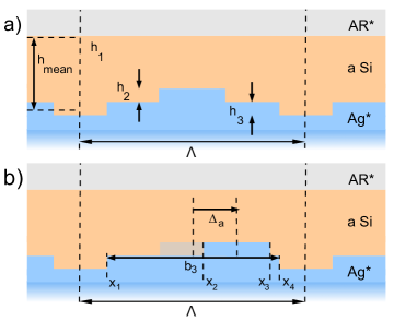
We limit our studies to perpendicular incidence and we only treat the absorption in the semiconductor layer, and note that the parasitic absorption in the metal layer will be discussed in a forthcoming publication. Furthermore, we confine our discussion to structures with two interfaces per layer, leading to a mirror symmetry in each grating layer, as shown in Figure 1. We benefit from this symmetry property to separate the eigenfunction space into symmetric and antisymmetric subspaces in each layer. As long as the entire structure retains the same mirror plane, then symmetric eigenfunctions do not couple to antisymmetric eigenfunctions. Since the zero order light incident perpendicular to the device belongs to the symmetric class, only symmetric eigenfunctions will couple to the incident light. As a coupling is induced between symmetric and antisymmetric eigenfunctions in different layers by asymmetric structures of the type shown in the lower panel of Figure 1, it is interesting to study whether asymmetric structures lead to improved light trapping, cf. Reference [8]. The simplifications made possible by geometrical symmetry and perpendicular incidence allow us to present results corresponding to resolutions that are a factor of two larger. We present our calculations with varying resolutions to provide a measure of the precision of such calculations and to assess the continuum limit.
In section 2, we outline the problem and our approach for its solution.
In section 3.1 we examine the absorption behavior in the semiconductor layer in a one-layer grating with rectangular geometry. Specifically, we look at a structure with an absorption free metallic substrate and an absorbing semiconductor layer with an antireflective cover. In particular we describe how the absorption extends to larger wavelengths as a function of grating depth, and we find an optimum depth for maximum absorption. This optimum depth is almost the same for both polarisations.
In Section 3.2 we investigate multi-layer staircase gratings that mimic sinusoidal gratings. Here we observe again that the optimum thickness for the grating structures does not differ much between the two polarisations. We note that with increasing number of grating layers for the same depth and structure, the spectra differ in some parts, while the integrated absorption is almost independent of the number of grating layers included. The absorption depends little on the period of the structure for both a rectangular and a stair-case sine grating.
In Section 3.3, we investigate asymmetric structures. In the simplest case, they consist of two symmetric layers with interfaces between the metal and the semiconductor. As layers are moved horizontally with respect to one another, symmetry of the entire structure is broken, as shown in Figure 1 b). As long as the symmetry axes for the two layers coincide, only the symmetric eigenfunctions are populated in each layer. But as soon as the symmetry is broken, symmetric eigenfunctions couple to antisymmetric eigenfunctions of different layers, and vice versa, such that all modes are populated. We investigate how these additional modes excited by the coupling between symmetric and antisymmetric eigenfunctions may increase absorption. Note that these symmetry considerations apply only to the case of perpendicular incidence.
The paper closes with a discussion of the observed effects and an outlook.
2 Method
In this section we first give a brief recapitulation of the calculational method [7]. Then we discuss the specific changes necessary for the present calculations.
Setup
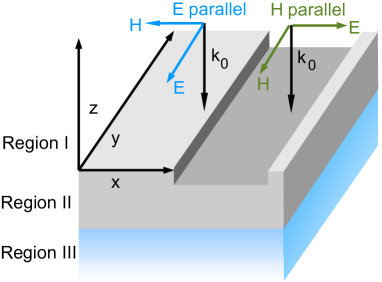
We split the diffraction problem into regions I-III, as shown in Figure 2, using the polarisation convention denoted there. We denote as either the electric field in the y-direction for E parallel polarisation or similarly the magnetic field in the y-direction for H parallel polarisation. In region I, we study the case of perpendicular incidence, that is the incident field can be written as
| (1) |
where and for regions I and III, the outgoing light can be written as a superposition of plane waves,
| (2) | |||||
| (3) |
where
| (4) |
Region II contains the diffraction grating consisting of layers, with thickness , where refers to the layer position within the grating.
Grating Problem
We briefly sketch our method for solving the grating problem, developed by one of us [7]. As we confine our study to perpendicular incidence, we note that the fields and do not depend on y. Within Region II, we briefly note that because of the lamellar structure, inside each layer the permittivity does not depend on the . Thus, a separation of variables becomes possible and the field can be written as a sum of products , the functions is an eigenfunction Helmholtz equation which needs to be solved within each grating layer. Because is piecewise constant, the Helmholtz equation can be written piecewise, too. For simplicity, we limit ourselves to two domains of different permittivity:
| (5) | |||||
| (6) |
Here, equation 5 refers to domain 1 and equation 6 refers to domain 2 and is -th eigenvalue of the Helmholtz equation in layer and and are the domain-wise parts of the the corresponding -th eigenfunction They need to fulfill a set of boundary conditions at interfaces in addition to the eigenvalue equations,
| (7) | |||||
| (8) |
for parallel polarised light in the limit , and likewise for parallel polarised light by replacing and by .
The electromagnetic field can then be expanded in terms of the eigenfunctions as a sum of modes propagating in between the adjacent layers,
| (9) |
where is the square root of the eigenvalue , with the sign convention that the imaginary part of be positive if it is non-zero. This sign definition ensures that the amplitudes () refer to eigenmodes that as functions of are exponentially decreasing (increasing), respectively.
The Helmholtz equation together with the sets of basis functions and the additional constraint of boundary conditions between the domains define the numerical eigenvalue problem for each grating layer . This method allows the calculation of a freely selectable number of eigenvalues and eigenfunctions to a precision limited only by machine number size: The electromagnetic field is infinitely many times differentiable inside each domain of constant permittivity, a fact that can be verified easily by repeated differentiation of the Helmholtz equation. If the functions are expanded in terms of polynomials that are orthogonal for inside the domain , one obtains exponential convergence in the number of included basis functions for eigenvalues and eigenfunctions. Thus, within a grating layer, our eigenmodes are obtained to the same precision as by analytic calculation following references by Botten et al. [9, 10, 11]. Note that the symmetry at perpendicular incidence together with the symmetry within the grating layer results in either purely symmetric or antisymmetric functions. If the basis functions are also either symmetric( antisymmetric) for even(odd) or odd ), half the number of coefficients defining the eigenfunctions will vanish, and therefore the symmetric eigenvalue problem can be formulated either for symmetric or antisymmetric case in terms of the non-zero variables and requires only of the numerical effort as it scales with the number of variables to the third power. For entirely symmetric structures, this property carries over to the solution of the radiation condition boundary value problem.
At the interface between grating layers, the field or has to satisfy the following continuity equations
| (10) | |||||
| (11) |
identically for and for , for H-polarisation and likewise for E-polarisation dropping the term . Inserting the expansion (9) leads to linear equations between the expansion coefficients of the upper layer and of the layer underneath. The fact that eigenmodes in the upper (lower) layer have discontinuities at positions where the eigenmodes in the lower (upper) layer are analytic, leads to a Gibbs phenomenon at , when eigenfunctions in the lower layer are expanded in terms of eigenfunctions in the upper layer. This gives rise to slow convergence and thus a large number of modes have to be included if the optical behaviour at such structures needs to be known accurately. This is the case even if the eigenmodes are known analytically. For H polarisation the convergence is substantially slower than for E polarisation because both the second and the first derivative in the direction perpendicular to the interface are discontinuous, whereas for E polarisation only the second derivative is discontinuous.
The substantial reduction in modes by fully exploiting symmetry and the stable implementation of the boundary value problem following [7] allows us to achieve the high resolution necessary to obtain reliable absorption spectra for such structures.
Anti-Reflective Coating
All the structures in this paper are calculated with an idealised artificial antireflective coating that almost completely eliminates reflection of the incident light at the top interface of the structure structure. We choose this setting, because we wish to describe an optimum limit for the absorption within the semiconductor layer, while the light is incident from outside. The antireflective coating used in our calculations consists of a homogeneous layer with an artificial material AR* whose refractive index is chosen wavelength dependent =, where is the refractive index of a-Si in the layer below, and the symbol stands for the real part. We take the antireflection coating to have a thickness corresponding to . Of course this is very artificial. However there exist realizations of antireflective structures which lead to similarly low reflexion losses [8],[12]. The broadband antireflection structure described therein consists of a rectangular grating with an additional coating with a lower refractive index than the grating below.
3 Results
3.1 rectangular gratings
Here, we look at gratings consisting of only one grating layer. Furthermore, we use an idealised, absorption free silver reflector whose permittivity is given by the real part of the permittivity of bulk silver, cf. Appendix.
The rectangular gratings are constructed like the ones shown in Figure 1, with a width of the metallic domain , and and nm, which stays constant while varying the grating layer thickness. Thus, the amount of semiconductor material is kept fixed. We also limit ourselves to grating depths that are at most about one third of the semiconductor layer thickness. Figure 3 shows the depth dependence of the absorption in a rectangular structure at the optimum period for the first absorption maximum of unpolarised light. In Figure 3 and the following similar figures, an integrated absorption of % corresponds to the absorption of all photons in the spectral range of nm up to nm, weighted with an AM-1.5 spectrum. We limit the spectral range of our studies to nm, where light trapping is most helpful, and the contribution of this region to the total absorption is limited to % for infinite thickness. Figure 3 shows that the maximum absorption for H parallel polarisation in the limited range of nm is almost %, whereas for E parallel polarisation it is %, and the optimum depth for both polarisations is close to nm. The figure also shows that the E parallel polarisation is fully converged, whereas for H polarisation the value is between % and %. To these values one may add a contribution of 38% for full absorption in the wavelength range from 350-550nm, if reflection is suppressed. Thus, the total absorption amounts to 62% for an ideal planar reflector, and if an ideal reflector in the shape of this rectangular grating is used, it is 75% for E polarisation and between 81.2 and 82.0 percent for H polarisation.
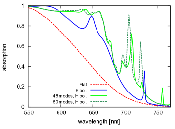
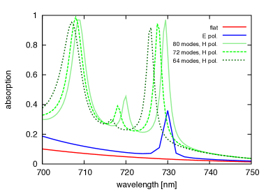
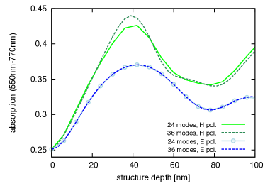
The spectrum in Figure 4 of the absorption shows that the grating leads to a spectral shift of the absorption edge, and the H parallel polarisation shows significantly more absorption, especially in the infrared region. We observe that even for weakly absorbing semiconductor layers, the strong resonances can lead to a noticeable increase in absorption. Note that Figure 4 shows that the region between and nm is highly sensitive. This behaviour is further investigated in Figure 5, which shows spectral mode dependence of high order calculations. Note how mostly the resonances move to higher wavelengths when increasing the number of modes for the calculation, such as the one at nm. The integrated absorption values for H-polarisation vary little for different mode numbers, even for small values of , as can be seen in Figure 3, as has been mentioned above. Due to the slow convergence we are unable to present absorption spectra for H polarisation in the limit of large . On the contrary, for E polarisation our spectra are well converged.
Figure 5 also shows how the background of the absorption spectrum, i.e. the broad absorption below the peaks clearly increases: It may be taken as near the nm resonance, and still around for the nm resonance. Such values would demand much greater thicknesses of a-Si, namely nm for the absorption value 0.3 at nm and even nm for the value 0.2 at nm, if instead of the grating a planar reflector is used. Thus, the effective thickness of the a-Si layer is increased by a factor of 3.5 at nm and about 6 at nm.
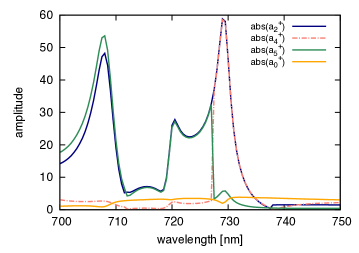
In the following, we take a closer look at the eigenmodes of the rectangular grating for which we have shown the spectrum in Figure 5. Figure 6 shows the amplitudes for the eigenmodes of the Helmholtz equation, sorted according to increasing imaginary part of the eigenvalue implying shorter decay length in the z-direction. The amplitudes are shown at the interface between the grating layer and the metallic reflector, and they result from solving the multilayer boundary value problem, with an incident amplitude , as defined in equation (1). Interestingly, the second and fourth eigenmodes are almost 60 times as much excited as the incident light, corresponding to a very high photon density near the bottom interface. We expect this excitation to become much weaker if losses in the metallic reflector are included. The fourth and fifth eigenmodes switch order near nm.
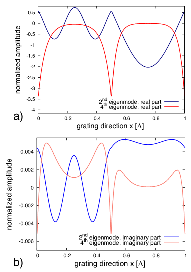
In Figures 7, we show the spatial behaviour of the strongly excited eigenmodes. Note how both modes display a sharp discontinuity at the interface between the two materials, as required by the boundary conditions. The structure of these modes shows clearly why the discontinuity of the first derivative gives rise to a strong Gibbs phenomenon leading to the excitation of evanescent waves of high order and consequently slow convergence as a function of the number of modes included in the expansion of the electromagnetic field. The comparatively small imaginary part in these eigenfunctions is the result of the rather weak absorptivity of a-Si at a wavelength of 729nm. We also note that a Fourier expansion of these eigenfunctions will not allow to correctly compute the absorption due to the 4-th eigenmode that mainly occurs in the vicinity of the interface. Here, the derivative of the imaginary part shows a dramatic discontinuity. Thus a Fourier expansion will converge only slowly in its vicinity. In view of the very large amplitude of this mode, the exact treatment of the boundary conditions at the a-Si-AG∗ interface as implented in our work is of particular relevance.
3.2 Mimicking sinusoidal gratings
Here, we want to study more complex structures, in particular we are interested in structures that mimic a sinusoidal grating. For that, we want an optimised grating structure, which is not defined by a number of parameters, but uniquely defined by a single parameter. This should facilitate changing the structure depth without altering the grating characteristics. To that end, we construct our grating structure as follows: We fix the layer thickness and interface positions by requiring that in each layer the excess area of the lamellar approximation above the sine cancels the missing area underneath it, and that the sum of excess areas is minimal and equal to the sum of missing areas. This minimization leads to a unique solution for and depending only on the number of layers , which we will refer to as pseudo-sine. The amount of semiconductor material is then identical for sine and pseudo-sine, see Figure 8.
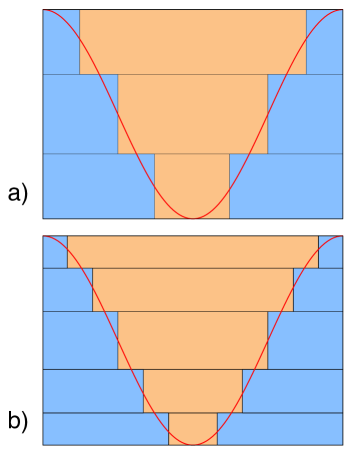
Figure 9 shows the integrated absorption for the interval between nm and nm, and how the first absorption maximum for both rectangular and pseudo-sine gratings only depends weakly on the period . In particular, we can see that the 5-step pseudo-sine offers more absorption, and that in both cases, the H polarisation is more readily absorbed. In Figure 9, the depth of and nm for the rectangular and for the pseudo-sine structure respectively are chosen close to the first absorption maximum for each structure type at around and nm as can be seen in Figures 3 and 10.
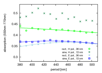
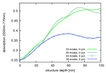
Figure 10 shows that the integrated absorption depends weakly on the number of modes used for the calculation, and in particular that for the E parallel polarisation, modes are sufficient to achieve convergence, whereas similar curves for H parallel polarisation are already in good agreement, but still varying for deep structures. It also shows a significant difference in optimum depth between polarisations, unlike for rectangular gratings, and that H parallel polarised light can be absorbed more effectively. When further comparing the depth dependence in Figure 10 with Figure 3, note that the optimum depth for a pseudo-sine structure is almost twice the optimum depth of the corresponding rectangular structure, and the optimum for the pseudo sine structure is much flatter with respect to varying depths.
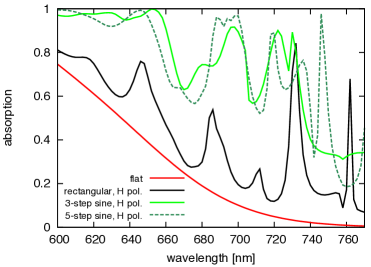
The spectra in Figure 11 and 12 show that the pseudo-sine gratings offer more absorption over the integrated spectral range when compared to the rectangular gratings, both by increasing the background absorption in the red and near infrared, and by exciting additional resonances.
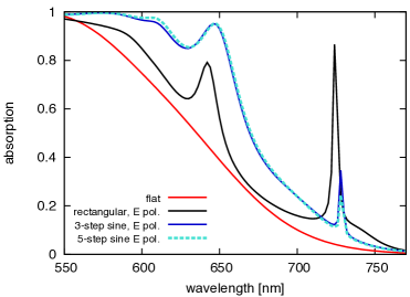
We note that the background absorption of the pseudo-sine grating without taking any peaks into account takes values of about 0.6 at nm and about 0.4 at nm. A device with a planar reflector would have to have an a-Si thickness of about nm at nm wavelength, and even nm at nm wavelength, i.e. 5 and 13 times the actual thickness of the device with the pseudo-sine grating.
For the pseudo-sine, the optimum parameters in terms of depth and period for the two polarisations are further apart when compared to a rectangular grating. The spectral comparison of 3-step and 5-step pseudo-sine gratings with period nm and depth nm in Figure 11 reveals that the spectra are almost identical for the E parallel polarisation. Thus the absorption spectra are almost independent of the number of layers chosen for the pseudo-sine approximation. This shows the validity of our geometrical argument for the unique choice of the pseudo-sine approximation. On the other hand, the same spectral comparison for the H polarisation in Figure 12 shows differing spectra for the 3 and 5-step pseudo-sine gratings, but they do share common spectral features, explaining the good convergence of the integrated absorption. Because both the mode number and the number of layers included are very limited, the pseudo-sine spectrum is not converged and must not be confused with the spectrum for a true sine grating, for which other methods such as the one pioneered by Chandezon et al. [13] will be required. The 5-step pseudo-sine grating shows a maximum integrated absorption in H polarisation of about 52%, while for unpolarised light it is given by the mean value from E- and H-polarisation and is about 45%. These values include the spectral range from 550-770nm. Adding the contribution of 38% from the wavelength range 350-550 nm, where light-trapping is not needed, we obtain a total of 90% for H polarisation and 83% for unpolarised light.
3.3 asymmetric gratings
In this section we show the benefits of asymmetry in the grating structure, as shown in Figure 1. All these results refer to the case of E-polarisation. The calculations for H-polarisation have not yet achieved the reliability that we require in this work. Further developments will be necessary to overcome these difficulties.
In Figure 13 we have calculated the depth dependence of a two-step pseudo-sine grating with period nm where one layer is shifted by from the symmetry axis, using 39 modes which is sufficient to display the high resolution limit behaviour. Figure 13 shows that the asymmetry improves the absorption from around % maximum to around %, and that the benefit of the asymmetric shift saturates if is increased beyond .
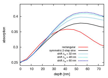
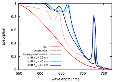
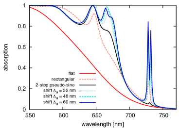
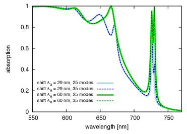
Figure 14 shows that for a structure with depth nm, the asymmetry not increases the background absorption into the red and near infrared, but also introduces additional resonances around nm and around nm, which correspond to the excitation of two antisymmetric eigenmodes of the grating. For comparison, the spectrum at a depth of nm in Figure 15 shows absorption resonances at the same wavelengths. To the maximum absorption of % observed for E-polarisation with this asymmetric grating integrated over nm we can add the absorption of 38% from nm, where light-trapping is not needed, and obtain a total absorption of 79%, quoted in the Abstract. Finally, Figure 16 shows the absorption in E-polarisation of a grating with period nm and depth nm calculated with and 35 modes. Despite large asymmetry, the spectra have well converged.
4 Discussion
We have investigated how much light can be trapped in a layer of a-Si with thickness 200 nm, which is typically used for a-Si solar cells, on top a metallic surface relief grating with one-dimensional (1-d) lamellar geometry. In order to obtain upper limits for the absorption, we have made the idealizations of a loss-free metallic reflector and a perfect antireflection coating. We have used a modal method with exact eigenfunctions to calculate accurate absorption spectra of such gratings. The absorption spectra for E polarisation of a sine-shaped diffraction grating approximated by lamellar gratings with 3 and 5 layers turn out almost identical, which is an interesting result. For such sine-like gratings, we have found that the limit of absorption is is about 90% for H-polarisation and about 75% for E-polarisation, compared to % for a planar reflector. We have also shown that an asymmetry in the grating structure generates additional peaks in the absorption spectrum and can thus increase the absorption.
In Section 3.1, we have shown that exact calculation of eigenmodes is particularly important as significant absorption occurs near interfaces where derivatives of the fields are discontinuous, see Figure 7.
While we have shown that in all cases studied, light-trapping in H-polarisation is significantly more effective than in E-polarisation, calculating fully converged spectra for H-polarisation remains difficult. The results presented in this paper have been made possible by making full use of the symmetry properties of the structures studied. One may hope that two-dimensional surface relief gratings of similar lamellar geometry will allow unpolarised light to be absorbed as effectively as H-polarised light is absorbed with the 1-d gratings, reported here. As already pointed out, our results are idealised in the sense that absorption in the metallic layer is suppressed. We expect that the peak height of absorption resonances will be strongly reduced by experimentally available metallic reflectors. On the other hand, one may hope that the background absorption below the peaks that is observed for all studied gratings, will still contribute significantly.
Acknowledgments
We acknowledge the financial support of this work by the Swiss Federal Office of Energy, and by the Paul Scherrer Institute. We also like to thank F.J. Haug and H.P.Herzig for helpful discussions and advice.
References
References
- [1] Shockley W and Queisser H J 1961 Journal of Applied Physics 32 510 ISSN 00218979
- [2] Yablonovitch E and Cody G D 1982 IEEE Transactions on Electron Devices 29 300–305 ISSN 0018-9383
- [3] Yu Z, Raman A and Fan S 2010 Proceedings of the National Academy of Sciences 107 17491–17496
- [4] Haug F J, Söderström K, Naqavi A and Ballif C 2011 Journal of Applied Physics 109 084516
- [5] Naqavi A, Söderström K, Haug F, Paeder V, Scharf T, Herzig H and Ballif C 2011 Opt. Express 19 128–140
- [6] Mokkapati S and Catchpole K 2012 Journal of Applied Physics 112 101101
- [7] Morf R 1995 JOSA A 12 1043–1056
- [8] Heine C and Morf R H 1995 Applied Optics 34 2476–2482
- [9] Botten I, Craig M, McPhedran R, Adams J and Andrewartha J 1981 Journal of Modern Optics 28 413–428
- [10] Botten L, Craig M, McPhedran R, Adams J and Andrewartha J 1981 Journal of Modern Optics 28 1087–1102
- [11] Botten L, Craig M and McPhedran R 1981 Journal of Modern Optics 28 1103–1106
- [12] Heine C, Morf R H and Gale M T 1996 Journal of Modern Optics 43 1371–1377
- [13] Chandezon J, Raoult G and Maystre D 1980 Journal of Optics 11 235
Appendix: permittivities of amorphous silicon and idealised silver
For our calculations we have employed dispersion data for amorphous silicon supplied by the PV-LAB of EPFL, Lausanne, Switzerland. To facilitate test calculations by the interested reader, we have used fit formulae to parameterize those measured data, valid for wavelengths m.
Denoting the complex refractive index by , and measuring wavelength in m, our fit functions for a-Si are given by
| (12) | |||||
| (13) |
The particular form for the imaginary part was chosen in order to properly describe the behaviour of the absorption constant in the infrared part of the spectrum.
Likewise, we use for our idealized a real dielectric constant parameterized by
| (14) |
where the wavelength is again measured in micrometers. Note that these fit functions are valid only for nm. We have used them for nm.