Unusual Shubnikov-de Haas oscillations in BiTeCl
Abstract
We report measurements of Shubnikov-de Haas (SdH) oscillations in single crystals of BiTeCl at magnetic fields up to 31 T and at temperatures as low as 0.4 K. Two oscillation frequencies were resolved at the lowest temperatures, Tesla and Tesla. We also measured the infrared optical reflectance and Hall effect; we propose that the two frequencies correspond respectively to the inner and outer Fermi sheets of the Rashba spin-split bulk conduction band. The bulk carrier concentration was cm-3 and the effective masses for the inner and for the outer sheet. Surprisingly, despite its low effective mass, we found that the amplitude of is very rapidly suppressed with increasing temperature, being almost undetectable above K.
pacs:
74.25.Ha, 74.78.-w, 78.20.-e, 78.30.-jManipulating the spin of electrons is of growing interest today, both for technological applications (spintronics) and for the realization of new, exotic states (triplet superconductivity; Majorana fermions). Topological insulators (TI) have emerged as promising candidates for the realization of these spin-related phenomena, owing to their edge states with spin protected by time-reversal symmetryHasan10 . Subsequently, it has been shown theoretically and discovered experimentally that in the V-VI-VII layered compounds BiTeX (with X = Cl, Br, I) the spin-orbit interaction can also lift the spin degeneracy of electrons, in a way similar to the effect of time-reversal symmetry at the surface of topological insulators, but this time in the bulk of non-centrosymmetric semiconductorsIshizaka11 ; Ermeev12 . The existence of surface states has also been established in these materialsErmeev12 ; Landolt12 ; Crepaldi12 . Theoretical work predicted that under pressure, BiTeI becomes a topological insulatorBahramy12 ; pressure-dependent optical spectroscopy experiment did confirm this predictionXi13 ; Tran13 .
Adding to the growing interest in the BiTeX compounds, a recent angle-resolved photoemission (ARPES) study discovered that BiTeCl is a topological insulator at ambient pressureChen13 . What makes it unique and exciting for the field is that, unlike all previous TIs where the crystal structure preserves inversion symmetry, BiTeCl is the first example of an inversion antisymmetric topological insulator (IATI). The inversion antisymmetry may give rise to other unusual effects, like a strong bulk polarization, topological magneto-electric effectFu07 , or topological superconductivityQi10 .
Motivated by these discoveries, we have measured the in-plane magnetoresistance, Hall effect, and optical reflectance of BiTeCl in order to investigate the electronic properties and Fermi surface of this IATI. Single crystals of BiTeCl were grown and characterized according to Ref.Arnaud13 . A sample of about 320.1 mm3 was cut from a larger piece and gold wires were attached using silver paint for electrical resistance measurements. The experiment was performed in Cell 9 at the National High Magnetic Field Laboratory. This facility combines a top loading 3He cryostat, with sample in liquid, and a 32 Tesla resistive magnet. Separate measurements of Hall effect were performed using a commercial PPMS system from Quantum Design. Room temperature optical reflectance data , at frequencies between 30 and 32 000 cm-1 (4 meV- 4 eV), were taken using a combination of a Bruker 113v Fourier spectrometer and a Zeiss microscope photometer. Then, Kramers-Kronig analysis was used to estimate the optical conductivity .
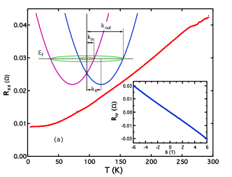
The upper panel of Fig. 1 shows the temperature dependence of the sample resistance. is metallic, with the resistance decreasing by a factor of about 4.5 upon cooling from room temperature to 5K. Hall data, shown in the lower inset of Fig. 1(a), shows that the carriers are electrons. We extracted a carrier concentration cm-3. Stoichiometric BiTeCl is a semiconductor with energy gap 220 meVChen13 ; however, the chemical potential in our sample is clearly into the conduction band, as in most Bi-based semiconductors.
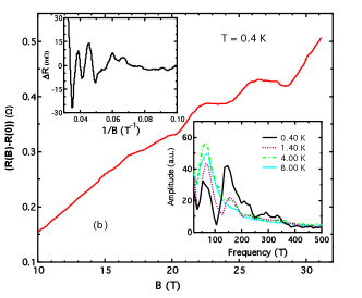
The lower panel of Fig. 1 shows the high magnetic field (above 10 T) in-plane magnetoresistance of BiTeCl at K. Oscillatory behavior becomes visible above 15 T. This behavior can be observed more clearly in the upper inset of Fig. 1(b), where we plot the data after subtracting a second order polynomial background. First, we notice the non-sinusoidal shape of the oscillations. We suggest that this complex behavior could be due to beating between two oscillation frequencies. Indeed, despite the observation of only a few oscillations, a Fourier transform of the data in Fig. 1(b) reveals two frequencies: T and T. The corresponding Fermi momentum in the -plane (using ) is Å-1 for and =0.068 Å-1 for , respectively. We notice that these values for the Fewrmi momentum are much smaller, by a factor of 3 at least, than those reported from ARPES data for the surface states of BiTeClChen13 . Instead, they seem to agree within the uncertainty of the chemical potential level with the results of band structure calculations for the bulkErmeev12 . Assuming that the frequencies originate from two 3-D Fermi surfaces, the resulting carrier concentration would be cm-3 for and cm-3 for , respectively. We notice that the concentration estimated using is nearly identical with that determined above from Hall effect, suggesting a common origin.
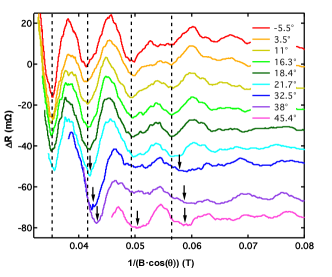
In Figure 2 we plot the angle dependent SdH oscillations at K as a function of the component of field perpendicular to the sample surface. At small angles, , the oscillations appear to scale with the normal component of the field. However, at higher angles, there is clear departure for the minima marked in the figure. This deiviation is indicative of a three-dimensional Fermi surface; moreover, it makes it unlikely that the oscillations originate from surface carriers. Were that the case, they would be highly two-dimensional, scaling precisely with the normal component of the magnetic field. Furthermore, a strong suppression of amplitude with tilting field is expected for surface oscillations, which does not appear to be the case in our data, at least up to . Experiments at higher magnetic field and larger tilting angle would help prove our conclusion more clearly.
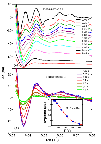
The temperature dependence of the quantum oscillations in BiTeCl is shown in Fig. 3(a). It can be clearly seen that the higher frequency, , is strongly suppressed with increasing temperature, being almost undetectable above K. In contrast, the low frequency () oscillations can be observed up to K. The lower inset of Fig. 1, displaying the Fourier transform of the SdH oscillations for several temperatures, illustrates the same thing. There is a rapid decrease of the amplitude with temperature and an enhancement of once is suppressed. Such behavior suggests that at low temperature the amplitude of oscillations is affected by the beating between the two frequencies, and once one is strongly damped with increased temperature, the other emerges more clearly.
We find the strong suppression of the amplitude with temperature puzzling. First, whether originates from bulk or surface carriers, it would imply a carrier effective mass much larger than previously observed and expected for these semiconductors, where in general , the free-electron mass. Second, repeating the experiment with different locations of the contacts (although still in the plane of the sample) we found the same situation, except that the frequency was even more strongly suppressed above 4 K. This suppression can be clearly seen in the main panel of Fig. 3(b), where we show the higher temperature (T4K) SdH oscillations for the second experiment. It appears that the data contain only one frequency (), and indeed, we found almost no hint of in the Fourier transform. While we do not have yet an explanation for this behavior, the presence of only one frequency, , allowed us to determine more accurately the temperature dependence of its amplitude and hence, its carrier effective mass . In the inset of Fig. 3(b) we plot the amplitude of the oscillation with minimum at T-1 versus temperature. A fit to the Lifshitz-Kosevich formulaShoenberg84 yields .
Given that both Hall effect and SdH oscillations may be affected, or even dominated, either by bulk or by surface carriers, we measured the infrared reflectance , as a true bulk probe. We showed previouslyMartin13 for the case of BiTeI that a monolayer-thick conducting surface layer with impedance affects the far-infrared reflectance of a conductor with conductivity of order cm-1 by less than 0.5%. Therefore, of BiTeCl, shown in Fig. 4(a), should be governed mainly by the response of the bulk carriers. A clear plasma edge can be observed around 500 cm-1 and in the limit 0, exceeds 90%, consistent with metallic behavior of the bulk.
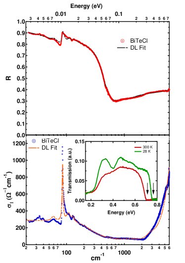
Clear phonon modes are observed at low frequency; they will be discussed elsewhere. Kramers-Kronig analysis of the reflectance yields the optical conductance, , shown in Fig. 4(b). A clear zero frequency (Drude) peak and sharp phonon modes are visible, as well as an absorption edge, at about 250 meV. The estimate of the semiconducting gap from optical reflectance is howevere strongly affected by the fact that the sample also trasmits light in the mid-infrared range, as it can be observed from our transmission measurements in the inset of Fig. 4(b). Within the uncertainty of the chemical potential with respect to the conduction band minimum, we find that the semiconducting gap is of the order of 760 meV, consistent with previous optical data Akrap14 . We notice also a similar interband transition to that observed and discussed in Ref. Akrap14 , situated at slightly higher energy, about 400 meV, in our sample. The dc conductivity is 300 , i.e. m-cm, characteristic of a moderately doped semiconductor. In order to extract the free carrier properties, we fit both and with a Drude-Lorentz modelWooten72 , optimizing the fit so that the same set of parameters reproduces best both quantities. The fit can be seen in both Fig. 4 (a) and (b). The Drude plasma frequency is cm-1 and the scattering rate cm-1.
On the one hand, if we consider the carrier concentration as determined from the Hall effect, which was identical with that resulting from the larger SdH oscillation frequency , then gives for the effective mass of the bulk the value . On the other hand, if were to assign to the lower frequency , then the resulting effective mass would disagree by almost an order of magnitude with that determined above from the Lifshitz-Kosevich formula. Therefore, it is more likely that the higher frequency originates from the same bulk conduction band that dominates the optical response. Furthermore, if this is the case, it makes even more unlikely that originates from the surface. First, let us recall that its Fermi momentum is much smaller than that measured previously for the surface states. Second, a smaller pocket for the surface than bulk is contradictory to both previous theoretical and experimental findings for the band structure of BiTeClChen13 ; Ermeev12 .
In conclusion, we have observed two SdH oscillations in our magnetoresistance data. Both originate from bulk Fermi sheets. The most likely scenario for BiTeCl is that they correspond to the inner and outer Fermi sheets of the Rashba spin-split bulk conduction band, as sketched in the inset in the upper panel of Fig. 1. In this case, according to the geometry illustrated in this diagram, we can determine the bulk Rashba momentum , as , where , the Fermi momentum of the outer band and , the momentum of the inner band, respectively. We find Å-1, which suggests that the Rashba momentum in BiTeCl is smaller by a factor of about 4.5 than that of BiTeI. The precise origin for the strong suppression of the amplitude of the higher SdH oscillation with temperature remains unknown. We suggest the possibility of oscillation beating between the two frequencies. Higher magnetic field experiments may help elucidate the question.
A portion of this work took place at the University of Florida, supported by the DOE through Grant No. DE-FG02-02ER45984. A portion was performed at the National High Magnetic Field Laboratory, which is supported by National Science Foundation Cooperative Agreement No. DMR-0654118, the State of Florida, and the U.S. Department of Energy. We thank Bobby Joe Pullum for support with the experiment at the National High Magnetic Field Laboratory. We also thank Dmitrii Maslov for stimulating discussions.
Note: While preparing our manuscript, we became aware of the posting of a similar work. Reference Xiang14 assigns the SdH oscillations to the surface states. However, here we provide compelling evidence in this work, taken at higher magnetic fields and lower temperatures, that the oscillations originate from the bulk Fermi surface of BiTeCl.
References
- (1) M. Z. Hasan and C. L. Kane, Rev. Mod. Phys. 82, 3045 (2010).
- (2) K. Ishizaka, M. S. Bahramy, H. Murakawa, M. Sakano, T. Shimojima, T. Sonobe, K. Koizumi, S. Shin, H. Miyahara, A. Kimura, K. Miyamoto, T. Okuda, H. Namatame, M. Taniguchi, R. Arita, N. Nagaosa, K. Kobayashi, Y. Murakami, R. Kumai, Y. Kaneko, Y. Onose, Y. Tokura, Nature Materials, 10, 521 (2011).
- (3) S. V. Eremeev, I. A. Nechaev, Y. M. Koroteev, P. M. Echenique, and E. V. Chulkov, Phys. Rev. Lett., 108, 246802 (2012).
- (4) G. Landolt, S. V. Eremeev, Y. M. Koroteev, B. Slomski, S. Muff, M. Kobayashi, V. N. Strocov, T. Schmitt, Z. S. Aliev, M. B. Babanly, I. R. Amiraslanov, E. V. Chulkov, J. Osterwalder, J. H. Dil, arxiv:1204.2196, (2012). (unpublished)
- (5) A. Crepaldi, L. Moreschini, G. Autès, C. Tournier-Colletta, S. Moser, N. Virk, H. Berger, Ph. Bugnon, Y. J. Chang, K. Kern, A. Bostwick, E. Rotenberg, O. V. Yazyev, M. Grioni, Phys. Rev. Lett., 109, 096803 (2012)
- (6) M. S. Bahramy, B.-J. Yang, R. Arita, and N. Nagaosa, Nat. Commun., 3, 679 (2012).
- (7) Xiaoxiang Xi, Chunli Ma, Zhenxian Liu, Zhiqiang Chen, Wei Ku, H. Berger, C. Martin, D. B. Tanner, and G. L. Carr, Phys. Rev. Lett., 111, 155701 (2013).
- (8) M. K. Tran, J. Levallois, P. Lerch, J. Teyssier, A. B. Kuzmenko, G. Aut s, O. V. Yazyev, A. Ubaldini, E. Giannini, D. van der Marel, A. Akrap, “Structural transition and collapse of the gap in BiTeI under pressure,” arXiv:1305.5485
- (9) Y. L. Chen, M. Kanou, Z. K. Liu, H. J. Zhang, J. A. Sobota, D. Leuenberger, S. K. Mo, B. Zhou, S-L. Yang, P. S. Kirchmann, D. H. Lu, R. G. Moore, Z. Hussain, Z. X. Shen, X. L. Qi, T. Sasagawa, Nature Physics, 9,, 704?708 (2013).
- (10) L. Fu, and C. L. Kane, Phys. Rev. B, 76, 045302 (2007).
- (11) X. L. Qi, T. L. Hughes, and S. C. Zhang, Phys. Rev. B, 81,134508 (2010).
- (12) J. Jacimovic, X. Mettan, A. Pisoni, R. Gaal, S. Katrych, L. Demko, A. Akrap, L. Forro, H. Berger, P. Bugnon, and A. Magrez, Scripta Materialia 76, 69 (2014).
- (13) D. Shoenberg, Magnetic Oscillations in Metals (Cambridge University Press, Cambridge, 1984).
- (14) C. Martin, E. D. Mun, H. Berger, V. P. Zapf and D.B. Tanner, Phys. Rev. B, 87, 041104(R) (2013).
- (15) Ana Akrap, Jérémie Teyssier, Arnaud Magrez, Philippe Bugnon, Helmuth Berger, Alexey B. Kuzmenko, and Dirk van der Marel, Phys. Rev. B, 90, 035201 (2014).
- (16) F. Wooten, Optical Properties of Solids (Academic Press, Inc., 1972).
- (17) F.X. Xiang, X.L. Wang, S.X. Dou, “Transport evidence of robust topological surface state in BiTeCl single crystals, the first strong inversion asymmetric topological insulator,” arxiv:1401.6732, (2014). (unpublished).