Colloquium: Graphene spectroscopy
Abstract
Spectroscopic studies of electronic phenomena in graphene are reviewed. A variety of methods and techniques are surveyed, from quasiparticle spectroscopies (tunneling, photoemission) to methods probing density and current response (infrared optics, Raman) to scanning probe nanoscopy and ultrafast pump-probe experiments. Vast complimentary information derived from these investigations is shown to highlight unusual properties of Dirac quasiparticles and many-body interaction effects in the physics of graphene.
pacs:
81.05.Uw, 73.20.-r, 03.65.Pm, 82.45.MpI Introduction
I.1 Scope of this review
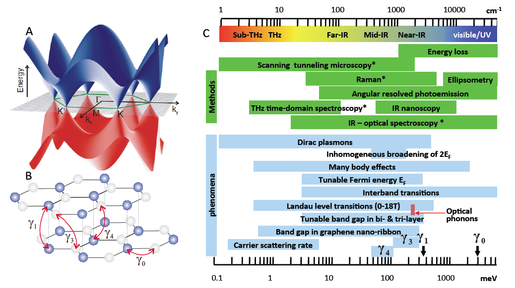
Graphene is a single atomic layer of -hybridized carbon atoms arranged in a honeycomb lattice. This two-dimensional (2D) allotrope of carbon is characterized by a number of superlative virtues Geim (2009), e.g., a record-high electronic mobility at ambient conditions Morozov et al. (2008), exceptional mechanical strength Lee et al. (2008a), and thermal conductivity Balandin et al. (2008); Ghosh et al. (2008) Remarkable properties of graphene have ignited tremendous interest that resulted in approximately 50,000 publications at the time of writing. A number of authoritative reviews111See Castro Neto et al. (2009); Peres (2010); Das Sarma et al. (2011); Kotov et al. (2012); Katsnelson (2012); McCann and Koshino (2013). have been written to survey this body of literature but no single review can any longer cover the entire topic. The purpose of this Colloquium is to overview specifically the spectroscopic experiments that have helped to shape the modern understanding of the physical properties of graphene. While selected topics in graphene spectroscopy have been discussed,222See Orlita and Potemski (2010) for optics, Ni et al. (2008b); Dresselhaus et al. (2012) for Raman scattering, Li and Andrei (2012) for scanning tunneling spectroscopy, and Connolly and Smith (2010) for other scanned probes. here we aim to present a panoramic view of physical phenomena in graphene emerging from both spectroscopy and imaging (Fig. 1C).
Spectroscopic observables can be formally categorized as either quasiparticle or current/density response functions. The former are fermionic, the latter are bosonic. The former is traditionally measured by photoemission and tunneling spectroscopy, while the latter can be investigated by, e.g., optical spectroscopy. Yet it may be possible to infer both quasiparticle and collective properties from the same type of measurements. For example, fine anomalies of the quasiparticle spectra seen in photoemission can give information about interactions between quasiparticles and collective modes (Sec. III.4) Conversely, optical conductivity, which is a collective response, enables one to infer, with some approximation, the parameters of a quasiparticle band-structure (Secs. III.1, II.2, II.3, and V).
Finding such connections is facilitated by spectacular tunability of graphene. For example, with photoemission or tunneling techniques one can monitor the chemical potential of graphene as a function of the electron concentration and thereby extract the thermodynamic density of states. The same physical quantity can be measured by a very different technique, the scanning single-electron transistor microscopy. In our analysis of such complementary data we focus on what we believe are the most pressing topics in the physics of graphene, e.g., many-body effects. Additionally, our review covers information obtained by scanned probes and out-of-equilibrium methods that greatly expand available means to study graphene in space and time domains. Finally, we briefly address phenomena that arise when physical properties of graphene are altered via its environment and nanostructuring.
I.2 Graphene morphology
Graphene can be isolated or fabricated in a number of different forms, which is an important consideration in spectroscopy. Effectiveness of a given spectroscopic tool depends on the accessibility of the sample surface to the incident radiation. The size of the accessible area must normally be larger than the wavelength of the incident beam unless near-field probes are employed (Sec. III.2) Mosaic structure and defects may affect momentum and energy resolution of the measurement. Graphene differs widely in terms of these parameters depending on preparation method. Mechanical exfoliation of graphite typically produces single, bi-, and multi-layer graphene (SLG, BLG, and MLG, respectively) of a few in size, although occasionally samples of dimensions of hundreds of can be obtained. Exfoliated samples can be transferred onto insulating substrates, after which they can be gated and subject to transport measurements. The sign and the magnitude of carrier concentration in gated samples can be precisely controlled over a wide range. The lower bound on is set by inhomogeneities (Sec. IV.1). The upper bound is limited by the dielectric breakdown strength of the substrate, although still higher are achievable by electrolytic gating .333See Mak et al. (2009); Xia et al. (2009b); Efetov and Kim (2010); Ju et al. (2011); Newaz et al. (2012). The carrier concentration can also be controlled by doping Chen et al. (2008).
Morphologically, exfoliated samples are single crystals. They hold the record for transport mobility although it varies much with the type of the substrate. Currently, high-quality hexagonal boron nitride (hBN) substrates enable one to achieve , which is about an order of magnitude higher than what is typical for graphene on SiO2 and corresponds to -scale mean-free path Dean et al. (2010); Mayorov et al. (2011b). The highest mobility is demonstrated by exfoliated graphene that is suspended off a substrate and subject to current annealing Du et al. (2008); Bolotin et al. (2008); Elias et al. (2011). Mechanical instabilities limit the size of suspended devices to – and restrict the maximum to a few times .
Large-area graphene can be made by another method: epitaxial growth on SiC by thermal desorption of Si van Bommel et al. (1975). Epitaxial graphene may contain a single or many dozens of layers. The initial layer (layer number ) has strong covalent bonds to the SiC substrate and is electronically different from the ideal SLG de Heer et al. (2007). The morphology and electron properties of the subsequent layers, , depend on which SiC crystal face it is grown: the Si-terminated face or the C-terminated face.444See Berger et al. (2004, 2006); Forbeaux et al. (1998); Charrier et al. (2002); Nagashima et al. (1993); Rollings et al. (2006); Ohta et al. (2006); Emtsev et al. (2009). According to de Heer et al. (2011), the Si-face grown graphene is orientationally ordered and has the Bernal stacking (as in graphite). The structure of the C-face epitaxial graphene is consistent with a stacking where every other layer is rotated by approximately with respect to a certain average orientation. The rotations inhibit interlayer tunneling so that the band structure of each layer is similar to SLG (see also Sec. IV.2).
The morphology of the epitaxial graphene after annealing resembles a carpet draping over the staircase Emtsev et al. (2009). It is characterized by domains a few wide and up to long that mirror the underlying SiC terraces Emtsev et al. (2009); de Heer et al. (2011).
The graphene/SiC interface is charged, inducing the -type doping of about in the first () graphene layer. Other layers have much smaller carrier concentration because of screening. The screening length of about one layer was measured by ultrafast infrared (IR) spectroscopy Sun et al. (2010a). The doping of the surface layers can be altered by depositing charged impurities Ohta et al. (2006); Zhou et al. (2008d). Relatively low mobility –, the inhomogeneity of the doping profile, and the lack of its in situ control can be seen as drawbacks of (the first generation of) epitaxial compared to exfoliated graphene. On the other hand, the much larger surface area of the epitaxial graphene is advantageous for spectroscopic studies and applications de Heer et al. (2007). An important recent breakthrough is epitaxial growth of graphene on high-quality hBN substrates Yang et al. (2013).
Graphene samples of strikingly large 30-in width Bae et al. (2010) can be produced by the chemical vapor deposition (CVD) on metallic surfaces, e.g., Ru,Ni or Cu that act as catalysts. CVD graphene can be transferred to insulating substrates making it amenable to gating and transport experiments Kim et al. (2009); Bae et al. (2010). The microstructure of CVD graphene sensitively depends on the roughness of the metallic substrate and the growth conditions. Typical structural defects of CVD graphene are wrinkles and folds induced by transfer process and also by thermal expansion of graphene upon cooling. Grain boundaries are other common defects that have been directly imaged by micro-Raman Li et al. (2010), transmission electron microscopy Huang et al. (2011), scanning tunneling microscopy Tapasztó et al. (2012); Koepke et al. (2013), and near-field microscopy Fei et al. (2013). The corresponding domain sizes range between –. On the other hand, graphene single crystals with dimension have been grown on Cu by CVD Li et al. (2011). Transport mobilities of CVD-grown graphene and epitaxial graphene on SiC are roughly on par.
At the opposite extreme of spatial scales are nanocrystals and nanoribbons. Graphene crystals of nm-size can be synthesized by reduction of graphene oxide555This can be done chemically Boehm et al. (1962); Dikin et al. (2007) or via IR irradiation El-Kady et al. (2012). or by ultrasonic cleavage of graphite in an organic solvent Hernandez et al. (2008); Nair et al. (2012). Laminates of such crystals can be of macroscopic size amenable to X-ray and Raman spectroscopy. Nanocrystals can also be grown epitaxially on patterned SiC surface de Heer et al. (2011). Graphene nanoribbons (GNRs) can be produced by lithography, nanoparticle etching, and unzipping of carbon nanotubes. There have been a number of spectroscopic studies of GNRs by scanned probes Tao et al. (2011), transport666See Han et al. (2007); Liu et al. (2009); Todd et al. (2008); Stampfer et al. (2009); Oostinga et al. (2010); Gallagher et al. (2010); Han et al. (2010)., and photoemission Siegel et al. (2008); Zhou et al. (2008a) but because of space limitations they could not be covered in this review.
I.3 Electronic structure of graphene neglecting interactions
In this section we summarize basic facts about the SLG band-structure within the independent electron approximation Castro Neto et al. (2009). The nearest-neighbor carbon atoms in SLG form bonds, which give rise to the and electron bands. The -bands are relevant mostly for electronic phenomena at energies . The unique low-energy properties of graphene derive from the -bands whose structure can be understood within the tight-binding model Wallace (1947). If only the nearest-neighbor transfer integral (Fig. 1B) is included, the amplitudes of the Bloch functions on the two triangular sublattices or of the full honeycomb lattice can be found by diagonalizing the Hamiltonian
| (1) |
where is the constant on-site energy, is the in-plane crystal momentum, represents the sum of the hopping amplitudes between a given site and its nearest neighbors, and Å is the lattice constant. The spectrum of has the form or
| (2) |
At energies , this dispersion has an approximately conical shape with velocity near the corners of the hexagonal Brillouin zone (BZ), see Fig. 1A. Only two of such corners are inequivalent, e.g., ; the other four are obtained via reciprocal lattice translations. Near the point, can be expanded to the first order in and — the components of vector parallel and perpendicular to , respectively. This expansion yields the 2D Dirac Hamiltonian
| (3) |
which prompts analogies between graphene and quantum electrodynamics Katsnelson and Novoselov (2007). Here , are the Pauli matrices. Expansion near points gives a similar expression except for the sign of the -term. The eigenvector of can be thought of as a spinor. The direction of the corresponding pseudospin is parallel (antiparallel) for energy (). The definite relation between the pseudospin and momentum directions is referred to as the chirality.
The conical dispersion yields the single-particle density of states (DOS) linear in . Accounting for the four-fold degeneracy due to spin and valley, one finds
| (4) |
The frequently needed relations between the zero-temperature chemical potential (referenced to the Dirac point energy ), Fermi momentum , and the carrier density read:
| (5) |
For not small compared to , deviations from the simplified Dirac model arise. The spectrum exhibits saddle points at energies , which are reached at the three inequivalent points of the BZ: and , see Fig. 1A. The DOS has logarithmic van Hove singularities at these saddle-points. In the noninteracting electron picture, direct () transitions between the conduction and valence band states of a given saddle-point would yield resonances at the energy . (Actually observed resonances are red-shifted due to interaction effects, see Sec. III.)
I.4 Many-body effects and observables
While the single-electron picture is the basis for our understanding of electron properties of graphene, it is certainly incomplete. One of the goals of the present review is to summarize spectroscopic evidence for many-body effects in graphene. In this section we introduce the relevant theoretical concepts. For simplicity, we assume that the temperature is zero and neglect disorder.
The strength of Coulomb interaction in graphene is controlled by the ratio
| (6) |
where is the effective dielectric constant of the environment. Assuming , for suspended graphene () one finds , so that the interaction is quite strong. Somewhat weaker interaction is realized for graphene on the common SiO2 substrate, . For graphene grown on metals the long-range part of the interaction is absent, with only residual short-range interaction remaining.
In general, spectroscopic techniques measure either quasiparticle or current (density) response functions. Within the framework of the Fermi-liquid theory Nozieres and Pines (1999) interactions renormalize the quasiparticle properties, meaning they change them quantitatively. The current/density response is altered qualitatively due to emergence of collective modes.
A striking theoretical prediction made two decades ago, González et al. (1994) is that Coulomb interaction among electrons should cause a logarithmically divergent renormalization of the Fermi velocity in undoped SLG,
| (7) |
which implies the negative curvature of the “reshaped” Dirac cones Elias et al. (2011). Here, is the high momentum cutoff and is again the momentum counted from the nearest Dirac point . The physical reason for the divergence of is the lack of metallic screening in undoped SLG because of vanishing thermodynamic density of states (TDOS) .
While Eq. (7) can be obtained from the first-order perturbation theory Barlas et al. (2007); Hwang et al. (2007b); Polini et al. (2007), the renormalization group (RG) approach of González et al. (1994) indicates that validity of this equation extends beyond the weak-coupling case . It remains valid even at albeit in the asymptotic low- limit where the running coupling constant is small. The RG flow equation underlying Eq. (7),
| (8) |
is free of nonuniversal quantities and , and so in principle it can be used to compare the renormalization effects in different graphene materials. The problem is that the asymptotic low- regime is hardly accessible in current experiments where one typically deals with the nonperturbative case . Theoretical estimates González et al. (1999); Son (2007); Foster and Aleiner (2008) of the -function in this latter regime yield
| (9) |
The corresponding renormalized velocity scales as
| (10) |
Distinguishing this weak power law from the logarithmic one (7) would still require a wide range of .
The gapless Dirac spectrum should become unstable once exceeds some critical value Drut and Lähde (2009); Khveshchenko (2001); Sheehy and Schmalian (2007). It is unclear whether this transition may occur in SLG as no experimental evidence for it has been reported.
In doped SLG the RG flow (8) is terminated at the Fermi momentum scale. Therefore, velocity renormalization should be described by the same formulas as in undoped one at but may have extra features at . This expectation is born out by calculations Das Sarma et al. (2007). The result for the Fermi velocity, written in our notations, is
| (11) |
where should be understood as . Comparing with Eq. (7), we see that is larger than in undoped SLG at the same momentum by an extra logarithmic term . This logarithmic enhancement of the Fermi velocity is generic for an electron gas with long-range Coulomb interactions in any dimension Giuliani and Vignale (2005). As a result, the renormalized dispersion has an inflection point near [see, e.g., Principi et al. (2012); Das Sarma and Hwang (2013)] and a positive (negative) curvature at smaller (larger) .
Renormalization makes the relation between observables and quasiparticle properties such as more complicated than in the noninteracting case. For illustration, consider three key spectroscopic observables: the single-particle DOS , the TDOS , and the threshold energy of interband optical absorption. Since for curved spectrum phase and group velocities are not equal, we must first clarify that by we mean the latter, i.e., the slope of the dispersion curve . In theoretical literature, is usually defined by the equation
| (12) |
where is the electron self-energy and the subscripts are suppressed to lighten the notations. In experimental practice (Sec. II.1), more directly accessible than is the spectral function
| (13) |
and the more convenient definition of is the energy at which has a maximum. As long as this maximum is sharp so that the quasiparticles are well-defined, the two definitions are equivalent. For the velocity, they entail
| (14) |
The three quantities in question, , , and , are related to as follows:
| (15) | ||||
| (16) | ||||
| (17) |
These formulas contain many-body corrections to the relations given in Sec. I.3 that enter through the derivatives of the self-energy, while Eq. (17) also has a vertex correction . For example, the DOS [Eq. (15)], measurable by, e.g., scanning tunneling spectroscopy (STS) is multiplied by the quasiparticle weight . Near the Fermi level one usually finds Giuliani and Vignale (2005), so that the interactions diminish the DOS. Inferring from using the formula of the noninteracting theory would cause overestimation of the Fermi velocity, e.g., by the factor of at Das Sarma et al. (2007). [In practice, the low-bias STS data may be influenced by disorder and finite momentum resolution, see Sec. II.1.] Away from the Fermi level the interaction may enhance rather than suppress . An example is the Dirac point region in a doped SLG where the DOS is predicted to be nonzero (U-shaped) LeBlanc et al. (2011); Principi et al. (2012) rather than vanishing (V-shaped).
Consider next the TDOS given by Eq. (16), which follows from Eqs. (14)–(15). The TDOS can be found by measuring capacitance between graphene and metallic gates, either stationary Ponomarenko et al. (2010); Yu et al. (2013) or scanned Martin et al. (2008). In the absence of interactions, the TDOS coincides with the DOS at the Fermi level. However, for repulsive Coulomb interactions the second term in the denominator of Eq. (16) is negative Giuliani and Vignale (2005). (This term can be written in terms of parameter of the Landau Fermi-liquid theory.) Hence, while is suppressed, is enhanced compared to the bare DOS. Extracting from Yu et al. (2013) may lead to underestimation.
The third quantity [Eq. (17)] stands for the threshold energy required to excite an electron-hole pair with zero total momentum in the process of optical absorption. Without interactions (see Fig. 2), and so the bare velocity is equal to . Using the same formula for interacting system Li et al. (2008) may lead to underestimation of the renormalized , for two reasons. First, is the group velocity at the Fermi momentum while the ratio gives the average phase velocity of the electron and hole at . If the dispersion has the inflection point near , as surmised above, the group velocity must be higher than the phase one. Second, the threshold energy of the electron-hole pair is reduced by the vertex (or excitonic) correction due to their Coulomb attraction.
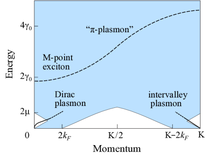
Let us now turn to the collective response of SLG at arbitrary and . The simplest type of such a process is excitation of a single particle-hole pair by moving a quasiparticle from an occupied state of momentum and energy to an empty state of momentum and energy . (The subscripts of all ’s are again suppressed.) The particle-hole continuum that consists of all possible points is sketched in Fig. 2. If the energy and the in-plane momentum of an electromagnetic excitation falls inside this continuum, it undergoes damping when passing through graphene. The conductivity has a finite real part in this region.
Collective modes can be viewed as superpositions of many interacting particle-hole excitations. A number of such modes have been predicted for graphene. Weakly damped modes exist outside the particle-hole continuum, in the three unshaded regions of Fig. 2. At low energy the boundaries of these triangular-shaped regions have the slope . Collective excitations near the -point (the left unshaded triangle in Fig. 2) are Dirac plasmons. These excitations, reviewed in Sec. III.2, can be thought of as coherent superpositions of intraband electron-hole pairs from the same valley. The excitations near the point (the right unshaded triangle) involve electrons and holes of different valleys. Such intervalley plasmons Tudorovskiy and Mikhailov (2010) are yet to be seen experimentally. Also shown in Fig. 2 are the “M-point exciton” that originates from mixing of electron and hole states near the -points of the BZ (Sec. I.3) and its finite-momentum extension, which is sometimes called by a potentially confusing term “-plasmon.”
Two other collective modes have been theoretically predicted but not yet observed and not shown in Fig. 2. One is the excitonic plasmon Gangadharaiah et al. (2008) — a single interband electron-hole pair marginally bound by Coulomb attraction. Its dispersion curve is supposed to run near the bottom of the electron-hole continuum. The other mode Mikhailov and Ziegler (2007) is predicted to appear in the range where . Unlike all the previously mentioned collective modes, which are TM-polarized, this one is TE-polarized. It is confined to graphene only weakly, which makes it hardly distinguishable from an electromagnetic wave traveling along graphene. Besides electron density, collective modes may involve electron spin. Further discussion of these and of many other interaction effects in graphene can be found in a recent topical review Kotov et al. (2012).
II Quasiparticle properties
II.1 Dirac spectrum and chirality
The first experimental determination of the SLG quasiparticle spectrum was obtained by analyzing the Shubnikov-de Haas oscillations (SdHO) in magnetoresistance Novoselov et al. (2005b); Zhang et al. (2005a). This analysis yields the cyclotron mass
| (18) |
and therefore the Fermi velocity . The lack of dependence of on the Fermi momentum in those early measurements was consistent with the linear Dirac spectrum at energies below .
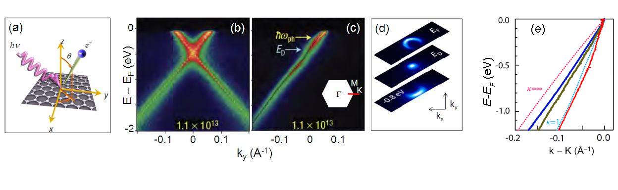
Direct mapping of the -band dispersion over a range of several eV Zhou et al. (2006); Bostwick et al. (2007b) was achieved soon thereafter by the angle-resolved photoemission (ARPES) experiments. This experimental technique, illustrated by Fig. 3(a), measures the electron spectral function [Eq. (13)] weighted by the square of the matrix element of interaction between an incident photon of frequency and an ejected photoelectron of momentum , see Eq. (19) below. The representative dispersion curves measured for epitaxial graphene on SiC are shown in Fig. 3(b) and (c), where red (black) color corresponds to high (low) intensity. The “dark corridor” Gierz et al. (2011) – along which one of the two dispersion lines is conspicuously missing, Fig. 3(c), occurs due to the selection rules for the matrix element known from prior work on graphite Shirley et al. (1995); Daimon et al. (1995). The full angular dependence of the ARPES intensity is depicted in Fig. 3(d).
The ARPES measurements have been carried out on epitaxial graphene grown on a variety of substrates, on free-standing samples Knox et al. (2011), and on multilayered samples with weak interlayer interactions Sprinkle et al. (2009). The tight-binding model (Sec. I.3) accounts for the main features of all these spectra. However, there are also subtle deviations. For example, the slope of the dispersion near the Dirac point varies systematically with the background dielectric constant [Fig. 3(d)], which is consistent with the theoretically predicted velocity renormalization, see Secs. I.4 and II.2. Certain additional features near the Dirac point (see Fig. 12) have been interpreted777See Zhou et al. (2007); Gao et al. (2010); Siegel et al. (2012); Walter et al. (2011c); Nagashima et al. (1994); Dedkov et al. (2008); Varykhalov et al. (2008); Himpsel et al. (1982); Enderlein et al. (2010); Sutter et al. (2009); Rader et al. (2009); Papagno et al. (2012). as evidence for substrate-induced energy gaps, Sec. IV.2. For graphene on SiC, an alternative explanation invokes electron-plasmon coupling Bostwick et al. (2007b), see Fig. 11 in Sec. III.4.
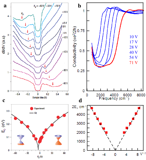
Complimentary evidence for the Dirac dispersion of quasiparticles comes the tunneling and thermodynamic DOS measurements by means of scanned probes. The Dirac point manifests itself as a local minimum marked by the arrows in the STS tunneling spectra of Fig. 4a. The U- rather than the V-shaped form of this minimum (Sec. I.3) is due to disorder smearing. The STS data obtained by Zhang et al. (2008b) (Fig. 4a) also exhibit a prominent suppression at zero bias for all gate voltages. To explain it Zhang et al. (2008b) proposed that this feature arises because of a limitation on the possible momentum transfer in tunneling. This limitation is lifted via inelastic tunneling accompanied by the emission of a BZ-boundary acoustic phonon of energy . This energy must be subtracted from the tip-sample bias to obtain the tunneling electron energy inside the sample. By tuning the electron density with a backgate Zhang et al. (2008b); Deshpande et al. (2009); Brar et al. (2010), one can change the Fermi energy with respect to the Dirac point . Taking the former as the reference point (i.e., assuming for now) one obtains the relation . As shown in Fig. 4c, thus defined is proportional to , as expected for the linear dispersion, Eq. (5). The same zero-bias gap feature is observed in other graphene samples studied by the Berkeley group, e.g., SLG on hBNDecker et al. (2011a). Yet it is not seen in STS experiments of other groups, see, e.g., Fig. 10(c), Sec. II.2, and Sec. II.3 below.888See also Deshpande et al. (2009); Li and Andrei (2012); Song et al. (2010); Xue et al. (2011); Yankowitz et al. (2012); Chae et al. (2012).
The dependence can be more directly inferred from the TDOS measured by the scanning single-electron transistor microscopy (SSETM) Martin et al. (2008). Unlike the STS spectra in Fig. 4a, the SSETM data are not obscured by the zero-bias feature. They show a finite and position-dependent TDOS at the neutrality point , reflecting once again the presence of disorder in graphene on SiO2 substrate, see also Sec. IV.1. The most definitive observation of the Dirac TDOS has been made using exfoliated graphene on hBN Yankowitz et al. (2012); Yu et al. (2013). Similar to SSETM, the TDOS was extracted from the capacitance measurements; however, it was the capacitance between the sample and the global backgate rather than between the sample and the local probe.
Let us now turn to the chirality of graphene quasiparticles. Recall that chirality refers to the phase relation between the sublattice amplitudes , , of the quasiparticle wavefunctions (Sec. I.3). The chirality has been independently verified by several techniques. First, it naturally explains the presence of the special half-filled Landau level at the Dirac point seen in magnetotransport Novoselov et al. (2005b); Zhang et al. (2005a). Next, in the STS experiments the quasiparticle chirality is revealed by the LDOS features observed near impurities and step edges, see Rutter et al. (2007); Mallet et al. (2007); Zhang et al. (2009a); Deshpande et al. (2009) and Sec. IV.1. The chirality influences the angular distribution of the quasiparticle scattering by these defects, suppressing the backscattering Brihuega et al. (2008); Xue et al. (2012), in agreement with theoretical predictions Ando et al. (2002); Katsnelson et al. (2006).
Finally, in ARPES the chirality manifests itself via the selection rules for the matrix element
| (19) |
that describes coupling of electrons to the vector potential of the photon. Here the Coulomb gauge is assumed and is the velocity operator. The matrix element depends on the relative phase of and . Based on symmetry considerations, the general form of at small must be
| (20) |
if spin-orbit (SO) interaction effects can be ignored. Here are the positions of th atom in the unit cell and is the nearest Dirac point. The coefficients and cannot be obtained solely from symmetry; however, regardless of their values, when is parallel (antiparallel) to for the states in the conduction (valence) band, the sum over in Eq. (20) vanishes and so does . This explains the low-intensity “dark corridor” in the observed ARPES signal, Fig. 3(c) and (d).
The ARPES selection rules are also relevant for BLG. Experimentally, the orientation of the low intensity directions rotates by () in SLG (BLG) when the photon polarization vector is switched between two orientations, parallel and perpendicular to Gierz et al. (2011); Hwang et al. (2011); Liu et al. (2011). Hwang et al. (2011) discussed how these rotation angles can be linked to the Berry phase — a quantity closely related to chirality — in SLG and BLG. However, their theoretical model for the matrix element has been a subject of controversy, which appears to be rooted in different assumption about the final state wavefunction in Eq. (19). At very high energies , the conventional approximation of by a plane wave should be adequate Shirley et al. (1995); Mucha-Kruczyński et al. (2008). In this case one can replace the velocity operator by leading to in Eq. (20). On the other hand, Hwang et al. (2011) replaced by the band velocity . This is perhaps appropriate at low energies at which near the graphene plane. The corresponding is equal to zero, which is admissible. However, diverges at , in contradiction to the perturbation theory Yu and Cardona (1999). In view of this problem and because other ARPES experiments and calculations Gierz et al. (2011) indicate a nontrivial -dependence of , further study of this question is desirable.
II.2 Renormalization of Dirac spectrum
Experimental verification of the many-body renormalization of the Dirac spectrum in graphene and its Fermi velocity in particular has been sought after in many spectroscopic studies. Some of these studies may be subject to interpretation because usually enters the observables in combination with other quantities, see Sec. I.4. In addition, when the change in is small, one cannot completely exclude single-particle effects.
Probably the first experimental indication for renormalization in graphene came from infrared absorption/transmission spectroscopy Li et al. (2008) of exfoliated SLG on amorphous SiO2 (a-SiO2). This study found that increases from to a higher value as the carrier density decreases from to , see Fig. 5d. Next came an STS study of Landau level spectra Luican et al. (2011b), which found a enhancement of (fifth row Table 1) in the same range of .
| Substrate | Method | Source | ||
|---|---|---|---|---|
| SiC (0001̄) | 7.26 | 1.15(2) | ARPES | Hwang |
| hBN | 4.22 | 2.0 | ARPES | Siegel |
| 1.20(5) | Capacitance | Yu | ||
| SiO2 | 1.80 | 2.5(3) | ARPES | Hwang |
| a-SiO2 | 2.45 | 1.47(5) | STS | Luican |
| Vacuum | 1.00 | 3.0(1) | SdH | Elias |
| 2.6(2) | Transport | Oksanen |
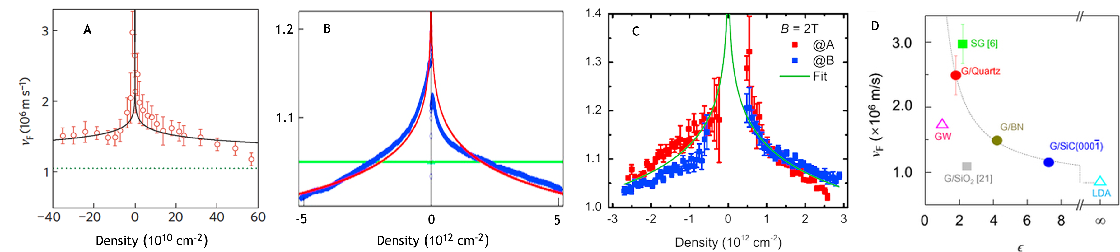
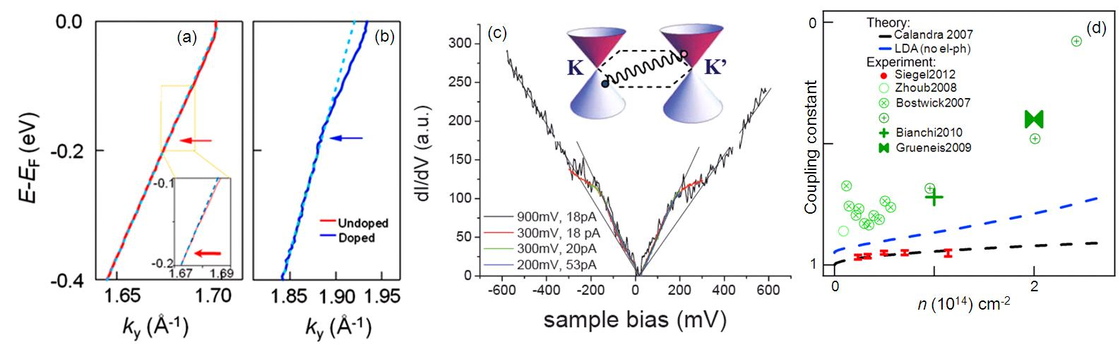
A much broader range of has been explored in suspended graphene where as small as a few times can be accessed. Working with such ultra-clean suspended samples, Elias et al. (2011) were able to carry out the analysis of the SdHO of the magnetoresistance over a two-decade-wide span of the carrier densities. This analysis yields the cyclotron mass [Eq. (18)] and thence . The Fermi velocity was shown to reach , the largest value reported to date, cf. Table 1. Elias et al. (2011) fitted their data (Fig. 5A) to Eq. (7) for undoped graphene by treating as an adjustable parameter. Figure 3 of Elias et al. (2011) suggests another possible fit, to Eq. (10) with the exponent , which is close to Eq. (9). It would be better to compare the measured with the theoretical predictions for doped graphene, i.e., with the extension (or extrapolation) of Eq. (11) to the case in hand, .
From the measurements of quantum capacitance (the quantity proportional to the TDOS) of SLG on hBN, Yu et al. (2013) found that increases by as varies from down to a few times , see Fig. 5B. The vertex corrections were not included when the conversion of the quantum capacitance to was done. Therefore, this number represents the lower bound on , see Sec. I.4.
Using substrates of different dielectric constant is another approach to study renormalization. An advantage of this approach is that a broad range of is not necessary in this case. Instead, the renormalization of velocity is driven by the change in the interaction strength where , see Eq. (7). A crude estimate of this effect is as follows. The dielectric screening by the substrate is effective at distances larger than the separation between graphene and the substrate. Hence, the momentum cutoff in Eqs. (7) and (11) should be chosen . If and , then and Eq. (7) entails
| (21) |
where we use “” to denote a change in a quantity. In a recent ARPES study Hwang et al. (2012a) the smallest was observed on metallic substrates. This number represents presumably the bare quasiparticle velocity in the absence of long-range Coulomb interactions. Note that it is close to the Fermi velocity measured in carbon nanotubes Liang et al. (2001). The ARPES results for three other substrates are reproduced in Fig. 5D. They clearly demonstrate a prominent velocity enhancement near the Fermi level. Thus, graphene on (the carbon face of) SiC has that is only slightly larger than what is observed for metallic substrates Siegel et al. (2011); Hwang et al. (2012a), which can be explained by the high . Graphene on hBN has close to that for SLG on a-SiO2, which is consistent with the effective dielectric constants of hBN and a-SiO2 being roughly equal Wang et al. (2012); Yu et al. (2013). A surprisingly large is found for graphene on crystalline SiO2 (quartz), see Table 1 and Fig. 5D.
As mentioned above, renormalization of the quasiparticle velocity in SLG can also arise from single-particle physics. One example is the modification of the electron band-structure by external periodic potentials Park et al. (2008d, c); Brey and Fertig (2009); Guinea and Low (2010); Wallbank et al. (2013). Such potentials are realized in moiré superlattices that form when graphene is deposited on lattice-matched substrates, which we will discuss in Sec. IV.3. Similar effects appear in misoriented graphene bilayers and multilayers that grow on the carbon face of SiC Hass et al. (2008) (Sec. I.2) and are also common in CVD graphene grown on Ni Luican et al. (2011a). Calculations predict a strong dependence of the velocity on the twist angle Bistritzer and MacDonald (2011); Trambly de Laissardiére et al. (2010); Lopes dos Santos et al. (2007); Shallcross et al. (2010); Lopes dos Santos et al. (2012). The experimental value of reported for twisted graphene layers on the carbon face of SiC is Crassee et al. (2011a); Miller et al. (2009); Siegel et al. (2011); Sprinkle et al. (2009). Changes of up to 10% among different layers for graphene on the carbon-face of SiC have been deduced from SdH oscillations de Heer et al. (2007) and magneto-optical measurements Crassee et al. (2011a, b). In the latter case these changes have been attributed to electron-hole asymmetry and also to variation of the carrier density and dielectric screening among the graphene layers. No variation of as a function of twist angle was observed by ARPES and STS Miller et al. (2009); Sprinkle et al. (2009); Siegel et al. (2011); Sadowski et al. (2006). However, a decrease of at small twist angles was found in the STS study of CVD graphene transferred to the grid of a transmission electron microscope Luican et al. (2011a).
II.3 Landau quantization
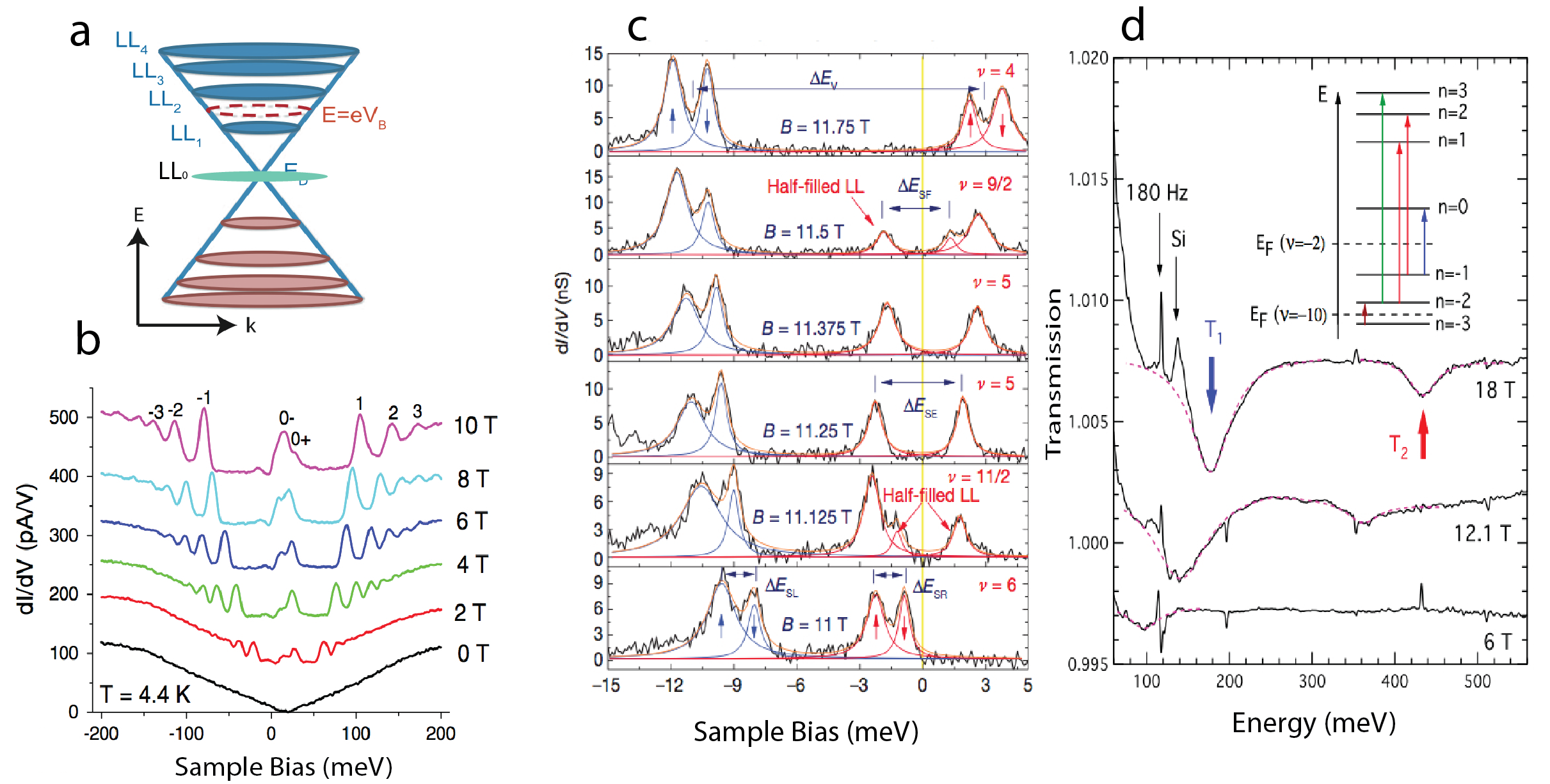
Spectroscopy of Landau level (LL) quantization in a magnetic field is yet another way to probe quasiparticle properties of graphene. The linear dispersion of SLG leads to unequally spaced LLs: (Fig. 6a), where or represents electrons or holes, respectivelyMcClure (1957); Gusynin and Sharapov (2006); Jiang et al. (2007). Each of the LLs has four-fold degeneracy due to the spin and valley degrees of freedom. Additionally, the electron-hole symmetric LL gives rise to the extraordinary “half-integer” quantum Hall effect Novoselov et al. (2005a); Zhang et al. (2005b), the observation of which back in 2005 was the watershed event that ignited the widespread interest in graphene.
The LL spectrum of graphene has been probed using scanning tunneling spectroscopy (STS), IR spectroscopy, and Raman scattering. The STS of graphene LLs was first carried out in graphene on graphite samples, where suspended graphene is isolated from the substrate at macroscopic ridge-like defect in graphite Li et al. (2009a). Figure 6b displays the differential conductance of graphene versus tip-sample bias at different magnetic fields normal to the graphene surface. Well defined LDOS peaks corresponding to discrete LL states appear in the tunneling spectra. These LL peaks become more prominent and shift to higher energies in higher magnetic fields consistent with the expected law. Similar LL spectrum was also observed in epitaxial grown graphene layers on SiC Miller et al. (2009).
To examine the fine structure within a LL, Song et al. (2010) performed high-resolution STS studies at temperatures as low as on epitaxial graphene. Figure 6c shows their data for the LL at the magnetic field range where the LL1 starts to cross the Fermi energy (yellow line). The LL1 level is composed of four separate peaks, indicating that the valley and spin degeneracy is lifted. The larger energy splitting () is attributed to the lifting of valley degeneracy. It increases monotonically with the applied magnetic field with the effective -factor of . The smaller splitting () has an average -factor close to , presumably due to the electron spin. Quantitatively, this spin splitting shows a highly unusual dependence on the filling factor. Comparing the spectra at filling factors of , , and , a clear enhancement of the spin splitting is observed at , which can be attributed to many-body effects (exchange enhancement). In addition, new stable half-filled Landau levels appear at half fillings such as and . Their origin is not yet clear. Landau level spectroscopy of graphene on SiO2 was presented in Luican et al. (2011b) and a similar study for graphene on hBN was reported in Chae et al. (2012). In the latter system, which has lower disorder, observation of many LLs was possible over a wide energy range. Deviations of the LL energies by about from the predictions of the single-particle theory were interpreted in terms of the Fermi velocity renormalization, see Fig. 5C. This is in line with the results of other measurements discussed above (Table 1).
The infrared (IR) spectroscopy provides another way to study the LL spectra Sadowski et al. (2006); Jiang et al. (2007); Henriksen et al. (2010). The IR transitions between LLs have to satisfy the selection rule , due to angular momentum conservation. Selection rules also apply to the circular polarization of light. As a result, graphene exhibits strong circular dichroism and Faraday effect Crassee et al. (2011b). Figure 6d displays the experimental data of normalized IR transmission spectra through SLG at several magnetic fields Jiang et al. (2007). The electron density is controlled so that Fermi energy lies between the and LL (inset in Fig. 6d). Two transmission minima and are readily observable. The resonance corresponds to the to intraband LL transition, and the resonance arises from the degenerate interband to and to transitions. The LL transition energies scales linearly with , as expected from the LL structure described above. A careful examination of the IR transitions as a function of electron filling factor further reveals that at zero filling factor, the to (or to ) transition is shifted to a higher energy compared to that at the filling factor of and Henriksen et al. (2010). This shift was again tentatively attributed to interaction effects.
III Current/density response and collective modes
III.1 Optical conductivity
Traditionally measured by optical spectroscopy, the “optical” conductivity quantifies the response of current to an external electric field in the low momenta region of the - parameter space, see Fig. 2. Both intraband and interband transitions contribute to the optical conductivity; we will start with the interband ones.
In a charge-neutral SLG, which is a zero-gap semiconductor with the Fermi energy at the Dirac point, the interband transitions have no threshold. Particularly interesting is the range of (IR) frequencies , where quasiparticles behave as massless Dirac fermions. Since the Dirac spectrum has no characteristic frequency scale and neither does the Coulomb interaction, at zero temperature and in the absence of disorder the conductivity must be of the form , where is defined by Eq. (6). [However, is, strictly speaking, a singular point Ziegler (2007).] For the noninteracting case, , the theory predicts999See Ludwig et al. (1994) for Dirac fermions in general and Ando et al. (2002); Gusynin and Sharapov (2006); Peres et al. (2006); Ziegler (2007); Falkovsky and Varlamov (2007); Stauber et al. (2008b) for SLG. , so that is real and has the universal value of
| (22) |
The corresponding transmission coefficient for suspended graphene is expressed solely in terms of the fine structure constant: .101010See Abergel et al. (2007); Blake et al. (2007); Roddaro et al. (2007); Ni et al. (2007). This prediction matches experimental data surprisingly well, with possible deviations not exceeding throughout the IR and visible spectral region Mak et al. (2008); Nair et al. (2008); Li et al. (2008). This implies that the interaction correction is numerically small even at . At the level of the first-order perturbation theory this remarkable fact is explained by a nearly complete cancellations between self-energy and vertex contributions Mishchenko (2008); Sheehy and Schmalian (2009); Sodemann and Fogler (2012)
Doping of graphene creates an effective threshold for interband absorption by the same mechanism as in the Burstein–Moss effect: the blue shift of the lowest energy of interband transitions in a doped semiconductor Yu and Cardona (1999). Due to Pauli blocking, no direct interband transitions exist at in the noninteracting electron picture, see Fig. 2. Experimentally, the existence of such a threshold has been confirmed by IR spectroscopy of gated SLG Wang et al. (2008b); Li et al. (2008); Horng et al. (2011). As shown in Fig. 4, the frequency position of the broadened step in scales as the square-root of the gate voltage , and so is proportional to . This is consistent with the linear dispersion of the Dirac quasiparticles. This behavior is seen in both exfoliated Li et al. (2008) and CVD-grown graphene Horng et al. (2011). At the smallest gate voltages, deviations from the square-root law are seen Li et al. (2008), which may be due to an interplay of many-body effects, the velocity renormalization and the vertex corrections, see Secs. I.4 and II.2.
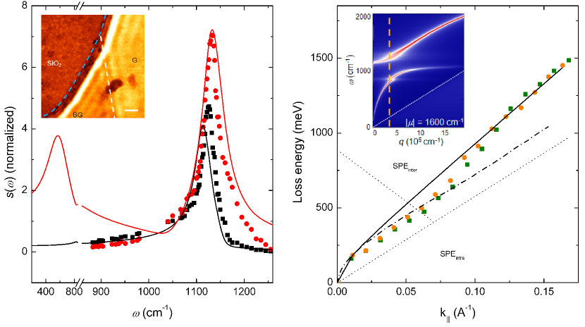
Vertex corrections (which are also referred to as the excitonic effects) play a prominent role also in the optical energy range –. The dominant spectroscopic feature in this region is the interband transition that connects electron and hole states near the -point of the Brillouin zone, where the DOS has van Hove singularities (Sec. I.3). This resonance is seen both in SLG and MLG samples.111111See Fei et al. (2008); Santoso et al. (2011); Mak et al. (2011); Kravets et al. (2010); Chae et al. (2011). This resonance has been detected by EELS and dubbed “-plasmon” [see, e.g., Eberlein et al. (2008)]. We prefer the term “-point exciton” to avoid confusion with the Dirac plasmon. Electron-electron interactions significantly renormalize the properties of this resonance. The position of the -point exciton is red shifted from the noninteracting value of by as much as in SLG samples Yang et al. (2009); Mak et al. (2011); Chae et al. (2011). The absorption peak has a Fano lineshape indicative of interaction effects.
Let us now discuss the intraband transitions. The commonly used Drude model assumes that the intraband response of a conductor is a simple fraction:
| (23) |
For noninteracting electrons with an isotropic Fermi surface one generally finds Ashcroft and Mermin (1976)
| (24) |
where is defined by Eq. (18). For Dirac electrons with and both and scale as . Parameter is known as the Drude weight. In the Drude model, the relaxation rate is frequency-independent and can be related to the transport mobility by . In exfoliated samples of typical mobility and carrier density one estimates . This is below the low-frequency cutoff of the IR microscopy Li et al. (2008). One can extend measurements to lower frequency provided larger area samples are used, such as epitaxial Choi et al. (2009); Hofmann et al. (2011) and CVD-grown graphene Horng et al. (2011); Rouhi et al. (2012); Ren et al. (2012). In both cases the gross features of the measured frequency dependence of IR conductivity comply with the Drude model. Note that such samples have relatively low mobility (Sec. I.2) and so show wider Drude peaks in .
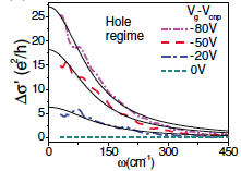
The intraband response as a function of the carrier density has been studied using a gated CVD-grown graphene Horng et al. (2011). The experimentally observed Drude weight was found to be 20–50% smaller than predicted by Eq. (24), see Fig. 7. The reduction was larger on the electron () side where the transport mobility was also lower. At the same time, the optical sum rule was apparently obeyed Horng et al. (2011). The conservation of the total optical weight was made possible by a residual conductivity in the interval , first observed by Li et al. (2008). In this region of frequencies both interband and intraband transitions should be suppressed yet the conductivity remains no smaller than , see Fig. 4b. Redistribution of the optical weight is common to correlated electron systems Millis (2004); Qazilbash et al. (2009); Basov et al. (2011), and so the residual conductivity of graphene is suggestive of interaction effects. Calculation of such effects is more difficult than for the undoped graphene but an extensive theoretical literature already exists on the subject. For example, the role of interaction in the conductivity sum rule was tackled in Sabio et al. (2008), the renormalization of was discussed in Abedpour et al. (2007); Levitov et al. (2013). The residual conductivity remains the most challenging problem. So far, theoretical calculations that consider electron-phonon121212See Stauber et al. (2008a); Peres et al. (2008); Hwang et al. (2012b); Scharf et al. (2013). or electron-electron131313See Grushin et al. (2009); Peres et al. (2010); Hwang et al. (2012b); Carbotte et al. (2012); Principi et al. (2013a). interactions predict relatively small corrections to inside the interbad-intraband gap . Such corrections can however be enhanced by disorder Kechedzhi and Das Sarma (2013); Principi et al. (2013b).
III.2 Plasmons
A plasmon is a collective mode of charge-density oscillation in a system with itinerant charge carriers. Plasmons have been extensively investigated both in classical and quantum plasmas. The dispersion relation of plasmons in a 2D conductor is given by the equation
| (25) |
where is the average of the dielectric functions of the media on the two sides, see, e.g., Fei et al. (2012); Grigorenko et al. (2012). At the -dependence of can be neglected, and so the plasmon dispersion is determined by the optical conductivity discussed above. This implies that , which is usually measured by optical spectroscopy, can also be inferred by studying plasmons Fei et al. (2012); Chen et al. (2012). (Actually, optics probes transverse rather than longitudinal response but at the two coincide.)
Note that is a complex number. Its real part determines the plasmon wavelength and the imaginary part characterizes dissipation. The condition for the propagating plasmon mode to exist is or , assuming is real. In SLG this condition is satisfied (both in theory and in experiment) at frequencies that are smaller or comparable to . In particular, at , one can use Eqs. (23) and (25) to express the plasmon dispersion in terms of the Drude weight :
| (26) |
This -behavior is a well-known property of 2D plasmons. Using (24) for with Eq. (18) for , one finds
| (27) |
The -scaling of the plasmon frequency at fixed should be contrasted with scaling well known for the 2D electron gas with a parabolic energy spectrum (2DEG). The difference is due to the dependence in the latter system. Another qualitative difference is the effect of electron interactions on . In 2DEG, interactions do not change , which is the statement of Kohn’s theorem Giuliani and Vignale (2005). In graphene, interactions renormalize the Drude weight Abedpour et al. (2007); Levitov et al. (2013), which causes quantitative deviations from Eq. (27). Qualitative deviations from this equation occur however only at where the plasmon dispersion curve enters the particle-hole continuum, see Fig. 2. At such momenta the Drude model (23) breaks down and a microscopic approach such as the random-phase approximation (RPA) becomes necessary Wunsch et al. (2006); Hwang and Das Sarma (2007); Jablan et al. (2009). The RPA predicts that inside the particle-hole continuum the plasmon survives as a broad resonance that disperses with velocity that approaches a constant value at large .
Experimental measurements of the plasmon dispersion over a broad range of have been obtained by means of electron energy loss spectroscopy (EELS). Such experiments141414See Liu et al. (2008); Liu and Willis (2010); Koch et al. (2010); Shin et al. (2011); Tegenkamp et al. (2011). have confirmed the scaling at small momenta and a kink in the dispersion in the vicinity of the particle-hole continnum. EELS study carried out by Pfnür et al. (2011) reported two distinct plasmon modes, a result yet to be verified through other observations.
The IR spectroscopy of graphene ribbons Ju et al. (2011); Yan et al. (2013) and disks Yan et al. (2012a, b); Fang et al. (2013) offered a complementary method to probe the plasmon dispersion. The experimental signature of the plasmon mode is the absorption resonance whose frequency is observed to scale as the inverse square root of the ribbon width (or disk radius ). This scaling agrees with the theoretical results relating to the plasmon dispersion in an unbounded graphene sheet [Eq. (26)]. For the ribbon, it reads Nikitin et al. (2011). The same relation can be deduced from the previous work Eliasson et al. (1986) on plasmons in 2DEG stripes. In fact, most of the results obtained in the context of plasmons in 2DEG in semiconductors Demel et al. (1990, 1991); Kukushkin et al. (2003) and also electrons on the surface of a liquid 4He Glattli et al. (1985); Mast et al. (1985) directly apply to graphene whenever the Drude model holds.
As shown theoretically and experimentally in that earlier work, the spectrum of plasmons in ribbons/stripes is split into a set of discrete modes dispersing as , as a function of the longitudinal momentum and the mode number , with having the meaning of the transverse momentum. Numerical results Eliasson et al. (1986); Nikitin et al. (2011) suggest that the phase shift parameter is equal to at . The resonance mode detected in graphene ribbons Ju et al. (2011); Yan et al. (2013) is evidently the mode. Probing modes in ribbons with conventional optics is challenging and has not been done is graphene [It may be possible with a grating coupler Demel et al. (1991).] On the other hand, working with graphene disks, one can effectively access the quantized values , where is the azimuthal quantum number. The observed mode Yan et al. (2012a, b); Fang et al. (2013) is evidently the dipolar one, , which has the highest optical weight. An additional mode that appears in both in ribbons and disks is the edge plasmon. We will talk about it at the end of this section where we discuss the effects of magnetic field.
The correspondence between the ribbon and bulk plasmon dispersions enables one to also verify the -scaling predicted by Eq. (27). This has been accomplished by electrostatic gating of graphene micro-ribbons immersed in ionic gel Ju et al. (2011) and monitoring their resonance frequency.
Plasmons in graphene are believed to strongly interact with electrons. Using the ARPES Bostwick et al. (2007b, a, 2010) observed characteristic departure of the quasiparticle dispersion from linearity near the Dirac point energy accompanied by an additional dispersion branch. These features, discussed in more detail in Sec. III.4, were interpreted in terms of plasmarons: bound states of electrons and plasmons Lundqvist (1967). Walter et al. (2011a, c) demonstrated that the details of the plasmaron spectrum are sensitive to dielectric environment of graphene. Carbotte et al. (2012) proposed that plasmaron features can be detected in near-field optical measurements, which allow one to probe the IR response at momenta .
Complementary insights on the interaction between plasmons and quasiparticles have been provided by the STS. Based on the gate dependence of the tunneling spectra, Brar et al. (2010) distinguished phonon and plasmon effects on the quasiparticle self-energy.
Plasmons in graphene strongly interact with surface phonons of polar substrates such as SiC, SiO2, and BN. Dispersion of mixed plasmon-phonon modes in graphene on SiC was investigated experimentally using high-resolution EELS Liu et al. (2008); Liu and Willis (2010); Koch et al. (2010) and modeled theoretically by Hwang et al. (2010). Theoretical dispersion curves Fei et al. (2011) for graphene on SiO2 are shown in the inset of Fig. 8b. The dispersion characteristic of mixed plasmon-phonon modes in nanoribbons measured via far-field IR spectroscopy was reported in Yan et al. (2012b, 2013).
In the near-field IR nanoscopy study of graphene micro-crystals on SiO2 Fei et al. (2011) the oscillator strength of the plasmon-phonon surface modes was shown to be significantly enhanced by the presence of graphene, Fig. 8a. The strength of this effect can be controlled by electrostatic doping, in agreement with theoretical calculations Fei et al. (2011).
Imaging of plasmon propagation in real-space Fei et al. (2012); Chen et al. (2012) [Fig. 8(left)] have led to the first direct determination of both real and imaginary parts of the plasmon momentum as a function of doping. In terms of potential applications of these modes, an important characteristic is the confinement factor , where is the plasmon wavelength and to the wavelength of light in vacuum. Experimentally determined confinement factor in exfoliated graphene Fei et al. (2012) was in the mid-IR spectral range . According to Eqs (27), the scale for the confinement is set by the inverse fine-structure constant, , with stronger confinement achieved at higher frequencies. The propagation length of the plasmons – is consistent with the residual conductivity measured by the conventional IR spectroscopy Li et al. (2008). Possible origins of this residual conductivity have already been discussed above, Sec. III.1. In confined structures one additional mechanism of plasmon damping is scattering by the edges Yan et al. (2013). Despite the observed losses, the plasmonic figures of merits demonstrated by Fei et al. (2012); Chen et al. (2012) compare well against the benchmarks set by noble metals. Even though surface plasmons in metals can be confined to scales of the order of tens of , their propagation length in this regime is plagued by giant losses and does not exceed for Ag/Si interface Jablan et al. (2009). This consideration has not been taken into account in a recent critique of graphene plasmonics Tassin et al. (2012). Further improvements in the figures of merits are anticipated for graphene with higher electronic mobility. The key forte of graphene in the context of plasmonics is the control over the plasmon frequency and propagation direction Mishchenko et al. (2010); Vakil and Engheta (2011) by gating.
The properties of graphene plasmons get modified in the presence of a transverse magnetic field . The magnetoplasmon dispersion is obtained from Eq. (25) by replacing with the longitudinal conductivity . For instance, instead of the Drude model (23), one would use its finite- analog, the Drude-Lorentz model Ashcroft and Mermin (1976), which yields another well-known dispersion relation Chiu and Quinn (1974)
| (28) |
This magnetoplasmon spectrum is gapped at the cyclotron frequency defined through the effective mass [Eq. (18)]. Equation (28) is valid at small enough where Landau quantization can be ignored. At large , quantum treatment is necessary. In the absence of interactions, the magnetoplasmon gap at is given by , the energy difference between the lowest unoccupied and the highest occupied Landau levels. Unlike the case of a 2DEG, where the Kohn’s theorem holds, renormalization of the Fermi velocity by interactions directly affects the cyclotron gap. This many-body effect has been observed by magneto-optical spectroscopy, Sec. II.3.
Probing finite- magnetoplasmons optically is possible via the finite-size effects, such as the mode quantization in graphene disks. As known from previous experimental Glattli et al. (1985); Mast et al. (1985); Demel et al. (1990, 1991); Kukushkin et al. (2003), numerical Eliasson et al. (1986), and analytical Volkov and Mikhailov (1988) studies of other 2D systems, the single plasmon resonance at splits into two. The upper mode whose frequency increases with can be regarded the bulk magnetoplasmon with , where is the disk radius. The lower mode whose frequency drops with can be interpreted as the edge magnetoplasmon, which propagates around the disk in the anti-cyclotron direction. Both the bulk-like and the edge-like modes have been detected by the IR spectroscopy of graphene disk arrays Yan et al. (2012a, b). Additionally, in epitaxial graphene with a random ribbon-like microstructure, the -field induced splitting of the Drude peak into a high- and a low-frequency branch was observed and interpreted in similar terms Crassee et al. (2012). The distinguishing property of the edge magnetoplasmon is chirality: its the propagation direction is linked to that of the magnetic field. This property has been verified in graphene systems by time-domain spectroscopy Petković et al. (2013); Kumada et al. (2013), which also allowed extraction of the edge magnetoplasmon velocity.
Other interesting properties of magnetoplasmons, such as splitting of the classical magnetoplasmon dispersion (28) into multiple branches have been predicted theoretically R. Roldán et al. (2009); Goerbig (2011) and their similarities and differences with the 2DEG case have been discussed. These effects still await their experimental confirmation.
III.3 Phonons
Raman spectroscopy is the most widely used tool for probing optical phonons in graphene and related materials Ferrari et al. (2006); Ferrari (2007); Dresselhaus et al. (2010, 2012). Quantitative studies of the Raman modes can provide rich information on graphene electron-phonon interaction, electronic structure, as well as on graphene layer thickness, edges, doping, and strain. Because graphene has the same bonding and hexagonal carbon lattice, its phonon band-structure is almost identical to that in graphite. Figure 9a shows calculated dispersion of the optical phonon branches in graphene (lines) Piscanec et al. (2004) as well as the experimental data of graphite (symbols) Maultzsch et al. (2004). One feature of these dispersions is the discontinuity in the frequency derivative at the and points in the highest optical branches. This discontinuity known as the Kohn anomaly arises from the unusual electron-phonon coupling in graphitic materials Piscanec et al. (2004).
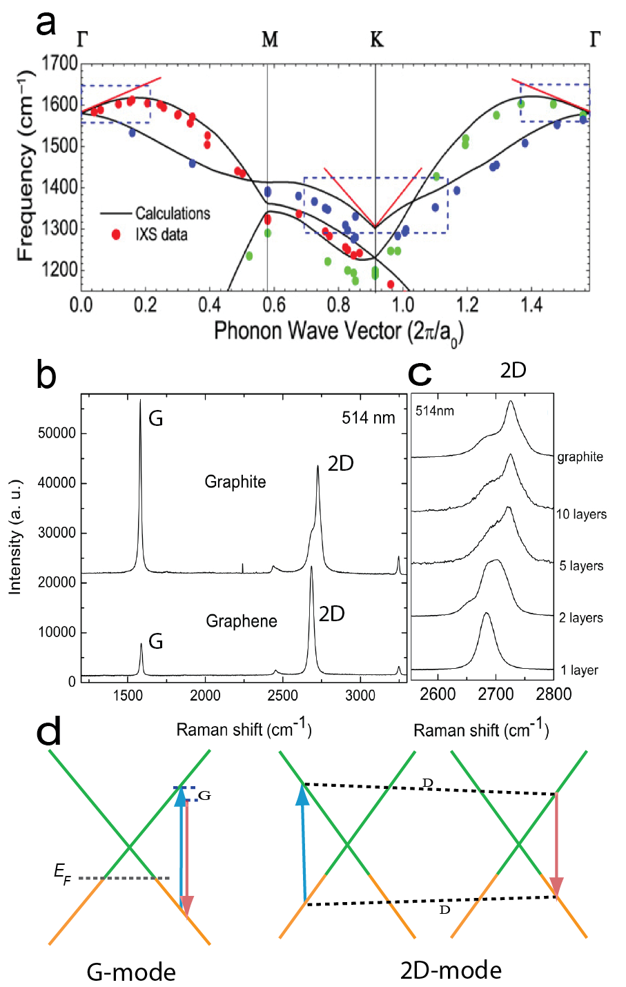
Figure 9b displays typical Raman spectra of SLG and graphite. They show the same qualitative Raman modes, with the two most prominent features being the -mode () and the -mode (, also known as mode). The other weak but very informative Raman feature is the -mode (). The lineshape of mode is very different in SLG, MLG, and graphite (Fig. 9c) Ferrari et al. (2006). As illustrated in Fig. 9d, the -peak arises from Raman scattering of the -point phonon. The -peak, on the other hand, is a two-phonon process involving emission of two -point optical phonons. The -peak is a double resonance process like the -peak. It requires structural defects to relax the momentum conservation constraint.
A detailed theory of the -mode Raman signal was presented in Basko and Aleiner (2008); Basko (2008); Basko et al. (2009); Basko (2009). The capability of controlling the electron Fermi energy through electrical gating helped to elucidate electron-phonon interactions Yan et al. (2007); Pisana et al. (2007); Malard et al. (2008); Das et al. (2008) and the quantum interference between different intermediate excitation pathways Chen et al. (2011); Kalbac et al. (2010). The frequency and linewidth of the Raman -mode reflect the energy and lifetime of the optical phonon at the point. The -point phonon experiences Landau damping by particle-hole excitations if its energy exceeds (see Fig. 2). As a result, the parameters of the Raman -mode depend on the carrier concentration, as demonstrated experimentally Yan et al. (2007); Pisana et al. (2007). The -mode Raman shows a reduced damping and a blue shift when the Fermi energy is larger than one half of the phonon energy, so that the phonon decay pathway into electron-hole pairs gets blocked. When the Fermi energy in graphene is increased further, some of the intermediate electronic transitions necessary for Raman scattering become blocked. This reduces destructive interference among different pathways and increases the -mode signal Chen et al. (2011).
The Raman scattering that gives rise to the mode involves emission of two BZ-boundary phonons close to the -point. Being a two-phonon process, it still has large intensity, which is explained by the triple-resonance mechanism (Fig. 9d), where every intermediate step involves a resonant electronic excitation Basko (2008); Basko et al. (2009). Due to smallness of the phonon energy compared with the incident photon energy , the momenta of the intermediate electron states are restricted to , where is the electron dispersion (Sec. I.3). The phonon momentum (relative to a -point phonon) then equals . Consequently, phonons and intermediate electronic transitions with specific momentum can be excited by varying incident photon energy for Raman modes. This allows one to map the dispersion of both the phonon and the electrons.
Once the phonon dispersion is known, Raman scattering can be used to probe electronic band-structure changes with a fixed laser excitation. For example, it can distinguish SLG, BLG, and MLG due to their different electronic dispersions Ferrari et al. (2006). In BLG and MLG there are several conduction and valence bands (Sec. V). Hence, valence electrons at more than one momentum can satisfy the relation. This leads to an apparent broadening and asymmetry of the Raman peaks for BLG and MLG, compared to those for SLG Ferrari et al. (2006).
The Raman -mode (short for the defect-mode) requires the existence of atomically sharp defects to provide the required momentum matching to scatter a zone boundary phonon close to -point. The intensity of the -peak is used to characterize the sample quality of graphene Malard et al. (2009); Dresselhaus et al. (2010); Ferrari (2007). The -mode is also useful for probing graphene edges, which can be considered as line defects. Experiments show that the -peak is indeed the strongest at graphene edges Graf et al. (2007); Gupta et al. (2009); Casiraghi et al. (2009), and that the -mode intensity is at maximum for light polarization parallel to the edge and at minimum for the perpendicular polarization Casiraghi et al. (2009). For ideal edges, theory predicts that the -mode Raman peak intensity is zero for zigzag edges but large for armchair ones Casiraghi et al. (2009). In addition to the effects discussed above, the intensity and frequency of Raman peaks also depend on the substrate Wang et al. (2008c); Ni et al. (2008a); *Ni2009uso; Lee et al. (2008b); Berciaud et al. (2008), temperature Calizo et al. (2007), and strain Yu et al. (2008); Proctor et al. (2009); Mohiuddin et al. (2009); Huang et al. (2009) through their effects on the phonon dispersion and electron Fermi energy.
III.4 Electron-phonon and electron-plasmon interaction
The energies and lifetimes of charge carriers in graphene are significantly affected by interactions with plasmons and phonons. The electron-phonon (el-ph) interaction results in a variety of novel phenomena discussed in Sec. III.3. The ARPES has been used to probe the signature of the el-ph interaction in the electronic spectra of graphene Bostwick et al. (2007b); McChesney et al. (2007, 2010); Zhou et al. (2008b) via the measurement of the quasiparticle velocity . The el-ph coupling constant is usually defined by Ashcroft and Mermin (1976). However, electron-electron (el-el) interaction also contributes to velocity renormalization (Secs. I.4 and II.2). Hence, thus defined gives a good estimate of el-ph coupling only if el-el interaction is screened, which is the case for graphene on a metallic substrate Siegel et al. (2011).
The el-ph interaction in graphene strongly depends on the carrier concentration, as shown in Fig. 10a,b. Siegel et al. (2011) have reported a large reduction of for quasi-free-standing graphene with close to the Dirac point . The overall reduction of the el-ph interaction can be reproduced by theoretical calculations Park et al. (2007). However, to account for the fine features of the quasiparticle dispersion, the el-el interaction has to be included Siegel et al. (2011); Zhou et al. (2008b); Lazzeri et al. (2008). At high doping appears to be enhanced, reaching values , and strongly anisotropic, similar to what is observed in graphite Zhou et al. (2006); Leem et al. (2008); Park et al. (2008a) and in the intercalated compound CaC6 Valla et al. (1999). Calandra and Mauri (2007b) argued these effects result from distortion of the graphene bands that hybridize with a new Ca-related band. On the other hand, Park et al. (2008b) suggested that the anisotropy of comes from the nonlinear band dispersion of the graphene bands at high doping.
From a high resolution ARPES study Zhou et al. (2008c) concluded that the electron-phonon coupling is dominated by the following phonon modes: phonon at approximately near the BZ corner, phonon () at the zone center, and the out-of-plane phonon at . Among these, the phonon is the one that mostly contribute to and mainly responsible for the kinks in the ARPES and in the tunneling spectra Li et al. (2009a), see Fig. 11b,c. The contribution of a specific phonon mode to can also be determined by studying how the Raman signal varies as a function of the applied magnetic field. These magneto-Raman studies focused on the phonon Faugeras et al. (2009, 2011), as the phonon is Raman inactive in high quality graphene samples.
The origin of the large discrepancy (Fig. 10d) between theoretically predicted and experimentally measured values of is debated.151515See Bianchi et al. (2010); Bostwick et al. (2007a); Park et al. (2008b, 2007); McChesney et al. (2007, 2010, 2008); Zhou et al. (2008c); Calandra and Mauri (2007a); Filleter et al. (2009); Grüneis et al. (2009). Siegel et al. (2012) found a good agreement with the theory (Fig. 10d) using the bare velocity measured for graphene grown on Cu where the el-el interaction is expected to be screened.
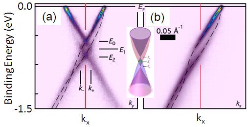
Electron-plasmon interaction is also believed to play an important role in renormalizing the band structure of graphene. Bostwick et al. (2007b, a, 2010) have argued that this interaction is responsible for the anomalous departure from the linear dispersion observed in epitaxial graphene grown on the Si face of SiC. Bostwick et al. (2010) have provided evidence (Fig. 11) for a well-resolved plasmaron band in the ARPES spectra of a “freestanding” graphene sample in which hydrogen has been intercalated between graphene and SiC to make negligible the interaction between the two. The plasmaron of momentum is a bound state of a hole with momentum and a plasmons of momentum Lundqvist (1967). Theoretical calculations Polini et al. (2008) within the approximation predict that the plasmaron band appears at finite charge densities. Its energy separation from the primary quasiparticle band is proportional to with a coefficient that depends on the Coulomb interaction strength , which in turn depends on the dielectric environment of graphene. Quantitative aspects of these calculations were disputed by Lischner et al. (2013) who included vertex corrections neglected in the scheme. Compared to Polini et al. (2008), for the same Lischner et al. (2013) find a broader plasmaron peak at a smaller separation from the primary band, which appears to be in a better agreement with the experiments of Bostwick et al. (2010).
No evidence of the plasmaron band has been reported in samples where decoupling of graphene from the buffer later was achieved by either gold or fluorine intercalation Walter et al. (2011b); Starodub et al. (2011). This has been attributed to a stronger dielectric screening by the buffer layer. An alternative interpretation of the apparent nonlinearity of the Dirac spectrum of graphene on SiC invokes a substrate-induced band gap Zhou et al. (2007, 2008c, 2008a); Benfatto and Cappelluti (2008); Kim et al. (2008), see Sec. IV.2 below.
IV Induced effects
IV.1 Inhomogeneities and disorder
Intentional and unintentional doping by charged impurities plays a very important role in the electronic phenomena of graphene. It is unclear if there is a single dominant source of unintentional doping even for most studied type of samples: exfoliated graphene on SiO2. In addition to adsorbates from the ambient atmosphere, doping could also result from charged defects in SiO2 Adam et al. (2007); Wehling et al. (2007); Schedin et al. (2007); Zhou et al. (2008d); Coletti et al. (2010) lithographic residues Dan et al. (2009), and metal contacts Connolly et al. (2010).
The dopants introduce not only a change in the average carrier concentration but also charge inhomogeneities and scattering. Near the graphene neutrality point inhomogeneities of either sign can arise, which are often referred to as the electron-hole puddles Geim and Novoselov (2007). Thus, even at the neutrality point the graphene is always locally doped. This is a qualitative explanation for nonvanishing conductivity Geim and Novoselov (2007); Tan et al. (2007); Chen et al. (2008) and TDOS Martin et al. (2008). A more detailed model Adam et al. (2007); Hwang et al. (2007a); Shklovskii (2007); Rossi and Das Sarma (2008) invokes a system of conducting electron-rich and hole-rich regions separated by - junctions Cheianov et al. (2007b); Zhang and Fogler (2008). The transport involves percolation through the and regions aided by tunneling across the junctions Cheianov et al. (2007a); Das Sarma et al. (2011). Many elements of this semiclassical model hark back to the earlier studies of two-dimensional Efros et al. (1993); Fogler (2004) and three-dimensional Efros and Shklovskii (1984) electron systems in semiconductors. However, the puddle model may not be quantitatively reliable for graphene. The correlation length of the density inhomogeneities is typically very short. For SLG on SiO2 it was consistently estimated to be of the order of using several complementary scanned probes microscopy techniques Deshpande et al. (2011); Luican et al. (2011b); Berezovsky et al. (2010); Martin et al. (2008). A typical electron-hole “puddle” is also too small to contain even a single charge Martin et al. (2008). Therefore, the inhomogeneities in question may be better described as quantum interference patterns of disorder-scattered electron waves rather than large semiclassical puddles. The situation may change if Coulomb interactions among electrons and impurities is screened. The crossover to the semiclassical regime is predicted to occur Fogler (2009) for graphene on a substrate of high dielectric constant . Suppression of density inhomogeneities in one graphene layer due to screening by a nearby second layer has been invoked to explain the observed localization transition in graphene-hBN-graphene structures Ponomarenko et al. (2011).
The inhomogeneities may also be induced by elastic strain and ripples Brey and Palacios (2008); Guinea et al. (2008b); Gibertini et al. (2010). Electron density inside the highly strained graphene bubbles Bunch et al. (2008); Levy et al. (2010); Georgiou et al. (2011) is undoubtedly inhomogeneous. However, the relation between strain and electron density is nonlocal. Indeed, no local correlations between the carrier density in graphene and the roughness of SiO2 substrate is evident in scanned probe images Martin et al. (2008); Deshpande et al. (2011); Zhang et al. (2009a).
The hypothesis that unintentional doping is caused by impurities trapped under graphene is supported by some micro-Raman experiments showing that proximity to the SiO2 substrate results in increase of carrier density Berciaud et al. (2008); Ni et al. (2009b); Bukowska et al. (2011). Yet other micro-Raman measurements Casiraghi et al. (2009) have not observed such correlations.
Charge inhomogeneities can be reduced by either removing the substrate Du et al. (2008); Knox et al. (2011) or using a high-quality hBN substrate Dean et al. (2010). The random charge fluctuations of exfoliated graphene on hBN are at least two orders of magnitude smaller than those on SiO2 according to the STM studies Xue et al. (2011); Decker et al. (2011b). (However, in such structures periodic charge oscillations may appear instead of random ones, see Sec. IV.3.) These random fluctuations are on par with the values estimated from transport data for free-standing graphene Du et al. (2008). The electronic mobility of graphene on hBN approaches implying the mean-free path of several hundreds nm Du et al. (2008); Dean et al. (2010).
Although detrimental for transport properties, impurities can play a role of elementary perturbations that help reveal useful physical information. We can give two examples. First, disorder-induced LDOS fluctuations seen in STS Rutter et al. (2007); Zhang et al. (2009a) reveal the dominant momenta for inter- and intra-valley scattering and therefore shed light on chirality and energy spectrum of the quasiparticles. Second, by utilizing ionized Co adatoms one can study screening properties of graphene. The screening cloud surrounding the adatoms was shown to have a qualitatively different profile depending on the total charge of the adatom cluster. In the sub-critical case this profile is governed essentially by the linear response dielectic constant of graphene. Theoretical modeling of the STS spectra Brar et al. (2011); Wang et al. (2012) suggests the enhanced value of this constant, which is indicative of many-body interactions Sodemann and Fogler (2012). In the super-critical case Wang et al. (2013) sharp resonances in the local DOS appear, which is the hallmark of a nonlinear screening with intriguing analogy to “atomic collapse” of super-heavy elements.
IV.2 Substrate-induced doping
Metallic substrates induce a strong doping of graphene, which is readily seen by the ARPES (Fig. 12a). The chemical potential measured with respect to the Dirac point ranges from approximately for Cu (111) Gao et al. (2010) and Cu films Siegel et al. (2012); Walter et al. (2011c) to for other transition metals, such as Ni (111) Nagashima et al. (1994); Dedkov et al. (2008); Varykhalov et al. (2008), Ru (0001) Himpsel et al. (1982); Enderlein et al. (2010); Sutter et al. (2009), and Co (0001) Rader et al. (2009). An exception to this is graphene on Ir (111) N’Diaye et al. (2006); Pletikosić et al. (2009), where the surface states of the substrate cause pinning of near zero.
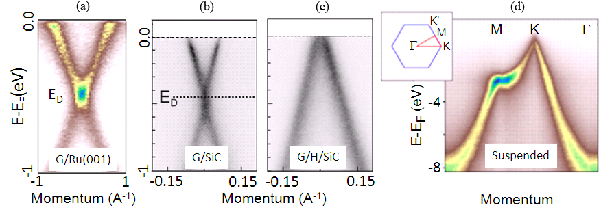
Naively, graphene is -doped if and -doped otherwise, where is the work function of pristine graphene and is that of the metal. In fact, the charge transfer is affected by chemical interaction between graphene and the metal and by their equilibrium separation Giovannetti et al. (2008). The amount of charge transfer can be modified by intercalation. Fluorine intercalation yields a large -type doping of graphene Walter et al. (2011b). Hydrogen intercalation leads to decoupling of graphene from the substrate Riedl et al. (2009), as evidenced by the ARPES dispersions, Fig. 12(b) and (c), typical of suspended graphene, cf. Fig. 12(d). Similar effects can be obtained by Au intercalation Gierz et al. (2008). When gold atoms are intercalated between graphene and a Ni (111) substrate Varykhalov et al. (2008), drops down to , corresponding to the two orders of magnitude decrease in the carrier concentration.
IV.3 Moiré patterns and energy gaps
When the lattice constants of the graphene layer and the substrate differ by a small relative amount and/or misoriented by an angle a moiré supelattice arises Marchini et al. (2007); N’Diaye et al. (2006); Wang et al. (2008a); Wintterlin and Bocquet (2009). The electron dispersion in the presence of the moiré superlattice gets modified as a result of hybridization of the original Dirac cones with their replicas folded into a superlattice Brillouin zone (sBZ). Such replicas have been seen in the ARPES spectra of graphene on Ir (111) Pletikosić et al. (2009) although they may also be due to the final-state diffraction Sutter et al. (2009).
The most striking experimental manifestations of the moiré superlattice effects have recently been observed in SGL on hBN. This system has , so that the moiré period can be as long as , which can be easily imaged by scanned probes (Fig. 13, insets). Dependence of the moiré period on the misorientation angle is very sharp, Fig. 13A, so achieving large period requires precise alignment.
It has been predicted theoretically that at the intersections of the replica and the main bands new Dirac points appear, Fig. 13C. For the practical case of a weak superlattice potential, these points have energy
| (29) |
where is the moiré period. [For the opposite limit of strong modulation, see Brey and Fertig (2009).] The extra Dirac points are characterized by a modified and generally, anisotropic quasiparticle velocity Park et al. (2008d); Guinea and Low (2010); Wallbank et al. (2013). The original Dirac point at the center of the sBZ remains gapless, at least, within the scope of generic theoretical models of the moiré superlattice which preserve sublattice symmetry.
First attempts to identify extra Dirac points in SLG/hBN structures were unsuccessful because these points were outside the experimental energy window Xue et al. (2011). In more recent experiments, which utilized precisely aligned () structures, the new Dirac points are clearly evidenced by additional minima of the DOS measured by STS Yankowitz et al. (2012), Fig. 13B. The unmistakable signatures of the second-generation Dirac points in transport include peaks in longitudinal resistance and the sign change of the Hall resistance Ponomarenko et al. (2013); Dean et al. (2013); Yankowitz et al. (2012); Yang et al. (2013), Fig. 13C and D. Additional Landau level (LL) fans emerging from these extra Dirac points are seen in magnetotransport Ponomarenko et al. (2013); Dean et al. (2013); Hunt et al. (2013) and the gate capacitance measurements. The detailed structure of such LLs is predicted to be fractal, as spectacularly illustrated by the iconic image of the “Hofstadter butterfly” Hofstadter (1976). Experiments Hunt et al. (2013) in strong fields demonstrate additional quantum Hall plateaus and a large gap (tens of meV) at the neutrality point, the physical origin of which remains to be understood.
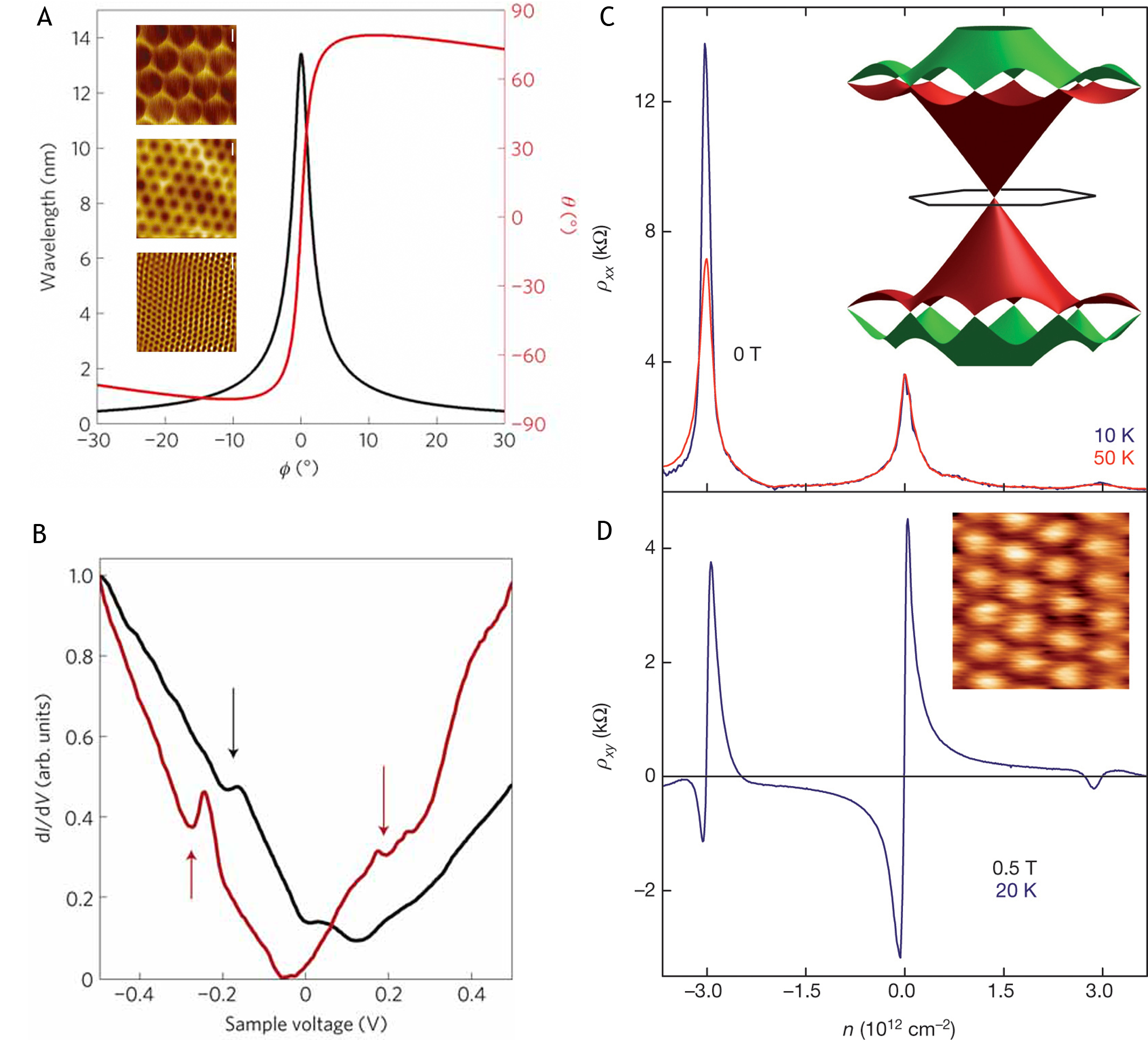
Opening a band gap at the Dirac point is indeed the most often cited effect that can enable wider applications of graphene. Inducing gap by confinement in various graphene superstructures such as quantum dots, ribbons, etc., has proved to be problematic due to disorder effects. Inducing a gap through graphene/substrate interaction seems an attractive alternative. The most straightforward mechanism of the gap generation is breaking the sublattice symmetry of graphene Brey and Fertig (2006); Giovannetti et al. (2007); Nakada et al. (1996); Nilsson et al. (2007); Trauzettel et al. (2007) For a hypothetical commensurate SLG/hBN structure, a band gap was predicted Giovannetti et al. (2007); Sławińska et al. (2010). Theoretically, the gap can also be induced by hybridization of the two valleys Mañes et al. (2007). A small band gap in graphene can also be induced by a spin-orbit coupling of Rashba type Kane and Mele (2005). The curvature of the graphene sheet is predicted to enhance the Rashba splitting Huertas-Hernando et al. (2006); Kuemmeth et al. (2008).
Existence of substrate-induced gaps have been indicated by many ARPES experiments. A very wide spread of gap values has been reported, which remains unexplained. One of the earliest ARPES studies Oshima and Nagashima (1997) claimed the largest gap so far, , for a “soft” SLG on TaC (111). Large gaps have also been reported for graphene on certain metallic substrates. Brugger et al. (2009) found gap for SLG on Ru (0001). Nagashima et al. (1994) observed – gaps in SLG on Ni (111) intercalated with alkaline metals. For Ru (0001) covered a with monolayer of gold Enderlein et al. (2010) and for Ir (111) substrates Starodub et al. (2011) the gap is . The effect of intercalants is counterintuitive because these are metals to which graphene interacts weakly. The gap for SLG on Cu is –. Zhou et al. (2007) made a case for the gap in epitaxial graphene on SiC. As discussed in Sec. III.4, a competing interpretation of these data is in terms of plasmarons Bostwick et al. (2007b, a, 2010). Comparable gaps were found for other semiconducting substrates Siegel et al. (2011); Walter et al. (2011c). For graphene on graphite the gap of Li et al. (2009a); Siegel et al. (2011) was reported. The STS Kawasaki et al. (2002) observed a for SLG/single-layer hBN/Ni (111) structure.
The largest Rashba splitting has been reported for graphene on magnetic substrate Ni (111) intercalated by Au Varykhalov et al. (2008). The mechanism behind this enhancement is still unknown. No Rashba splitting has been observed on another magnetic substrate, Co (0001) intercalated by Au Rader et al. (2009). Although intrinsic spin-orbit (SO) coupling is also responsible for the opening a band gap, , in pure SLG it is predicted to be extremely small, e.g., – Kane and Mele (2005). A broken symmetry at the interface of two SLG can somewhat amplify this gap Schmidt and Loss (2010). Impurities in graphene resulting in type deformation of the flat graphene are also predicted to enhance up to Castro Neto and Guinea (2009). In fact, a recent experimental study on hydrogenated graphene revealed a drastically enhanced of Balakrishnan et al. (2013). Alternatively, the interactions of charge carriers in graphene with heavy atoms such as In and Tl adsorbed on graphene are predicted to enhance up to and , respectively Weeks et al. (2011).
IV.4 Elastic strain
A controlled uniaxial strain can be readily introduced into graphene by stretching the flexible substrate. The strain modifies graphene phonon energy spectrum, which is effectively probed by Raman spectroscopy. Under uniaxial strain the and phonon bands display significant red shift proportional to the applied strain: a result of the anharmonicity of the interatomic potentials in graphene Ni et al. (2008a); *Ni2009uso; Huang et al. (2009); Mohiuddin et al. (2009); Tsoukleri et al. (2009). Meanwhile the bonds of graphene lengthen/shorten in the direction parallel/perpendicular to the strain axis. This reduces the symmetry of the honeycomb lattice to , and splits the doubly degenerate band into two singlet bands, and , with normal modes perpendicular and parallel to the strain axis, respectively. The polarization of Raman scattered light for the and modes is thus expected to depend on the direction of the strain axis relative to the crystal orientation: a conjecture verified by Huang et al. (2009) and Mohiuddin et al. (2009).
Strain also introduces profound modifications to graphene electronic structure. The defining topology feature of graphene electronic band, namely the degeneracy of conical electron and hole bands at Dirac points, is protected by the inversion symmetry of graphene lattice Hasegawa et al. (2006); Kishigi et al. (2008); Wunsch et al. (2008). A small perturbation in form of mechanical strain does not lift the degeneracy, but deforms the energy bands and shifts the Dirac points in both the energy and the momentum space. The former is equivalent to a scalar potential also known as the deformation potential. A general nonuniform strain generates a spatially varying dilation of the graphene lattice and therefore local ion density. The deformation potential arises because the corresponding Coulomb potential is only partially screened by electrons Suzuura and Ando (2002); Kim and Castro Neto (2008); Guinea et al. (2008a). Next, shifting the Dirac point in the -space away from the () points Pereira and Castro Neto (2009); Farjam and Rafii-Tabar (2009); Ni et al. (2008a); *Ni2009uso; Dietl et al. (2008). is analogous to the effect induced by an external magnetic field applied perpendicular to the graphene plane. One can parametrize the mechanical strain by a gauge field Iordanskii and Koshelev (1985); Kane and Mele (1997); Sasaki et al. (2005); Morpurgo and Guinea (2006); Katsnelson and Novoselov (2007); Fogler et al. (2008) and define the pseudomagnetic field . The strain-induced and have opposite signs at two valleys and , so that the time-reversal symmetry is preserved.
It is possible to engineer a special nonuniform strain for which is approximately constant in a finite-size region. If such pseudomagnetic field is strong enough, it can lead to Landau quantization and quantum Hall-like states Guinea et al. (2010b, a). In a recent experiment Levy et al. (2010), such an unusual Landau quantization has been observed in highly strained graphene nanobubbles. The strain arises upon cooling because of a mismatch in the thermal expansion coefficients of graphene and the Pt substrate (Fig. 14A). The pseudo-Landau levels, manifested as local density of states peaks, are probed by STS (Figs. 14B and C). Their energies follow the theoretically predicted behavior with a gigantic , see Fig. 14C.
IV.5 Photo-induced effects
Optical spectroscopy with ultrafast laser excitation pulses provides a unique tool to probe the dynamic evolution of electrons and phonons in graphene, including the cooling of the non-equilibrium quasiparticle plasma through electron-electron and electron-phonon interactions and the relaxation of hot optical phonons. These processes are not only of fundamental interest due to the unusual electronic structure in graphene, but also important for technological applications of high-field electronics and nonlinear photonic devices Xia et al. (2009a); Bao et al. (2009); Zhang et al. (2010); Sun et al. (2010b); Bonaccorso et al. (2010).
Response of graphene to a pulsed laser excitation has been studied by several complementary ultrafast spectroscopy techniques. For example, pump-probe IR/visible spectroscopy Sun et al. (2008); Dawlaty et al. (2008); Newson et al. (2009); Huang et al. (2010) and pump-probe THz spectroscopy George et al. (2008) has been employed to track the time evolution of optical absorption and transmission by graphene. Ultrafast photoluminescence Lui et al. (2010); Liu et al. (2010); Stöhr et al. (2010) has been used to monitor light emission by non-equilibrium electron gas. Time-resolved Raman spectroscopy Yan et al. (2009); Chatzakis et al. (2011) has explored generation and decay of hot optical phonons. Breusing et al. (2009) studied graphite using pump pulses and a broadband probe pulses with energy spectrum from to . Figure 15a shows the observed increase of transmission during the first with sub- time resolution. This phenomenon is attributed to partial Pauli blocking of the optical transition by photo-excited electron-hole pairs. The change in transmission scales linearly with the pump influence and decays with two time constants of and . The former characterizes electron-electron interactions, which cause energy redistribution within the conduction and valence band, as well as relaxation of occupation factors by Auger processes. The second time constant describes interaction of quasiparticles with optical phonons. The emission of optical phonons with energy cools down electron-hole plasma. Once its temperature drops below this number, emission of optical phonons becomes ineffective. Eventual equilibration of the electron and lattice temperatures is achieved by emission of acoustic phonons on a time scale of .
The decay dynamics of graphene in the temporal range is shown in Fig. 15b with three different probe photon energies. In addition to the fast decay processes described above, it shows a slower relaxation process with a time constant of . This picosecond time scale reflects partial thermalization between the hot electron/holes and optical phonons with the acoustic phonons in graphene. We note that the photo-induced transmission change can become negative at certain probe photon energies at longer delay. This is because optical excitation not only leads to Pauli blocking of interband transitions, but also increased high frequency absorption from intraband transitions. At longer pump-probe delay, the intraband absorption can dominate over the Pauli blocking effects at some probe photon energies. Similar photo-induced transmission decreases have also been observed in optical pump-THz probe measurements, where photo-induced intraband transitions always dominate George et al. (2008); Strait et al. (2011); Wright et al. (2009).
Ultrafast photoluminescence monitors the light emission from the highly non-equilibrium electrons after femtosecond pump excitations Lui et al. (2010); Liu et al. (2010); Stöhr et al. (2010). Broad light emission across the visible spectral range (–) was observed with femtosecond near-IR laser excitation, where the incident photon has an energy of . This unusual blue-shifted photoluminescence exhibits a nonlinear dependence on the laser fluence, and it has a dominant relaxation time within . This nonlinear blue-shifted luminescence was attributed to recombination of hot electron-hole plasma generated right after the femtosecond excitation.
In addition to the electron dynamics, researchers were able to probe the phonon dynamics specifically using time-resolved Raman spectroscopy Chatzakis et al. (2011); Yan et al. (2009). Such studies show a decay lifetime of for the BZ-center -mode phonons. This time scale corresponds to the cooling of the optical phonons through anharmonic coupling to acoustic phonons, and the time constant is similar to that obtained in pump-probe transmission spectroscopy.
V Bilayer and multilayer graphene
There has been a rapidly increasing interest in graphene systems with more than one layer (for an early review, see Nilsson et al. (2008)). The electronic structure of BLG and MLG is distinctly different from that of SLG. These differences give rise to many new phenomena, ranging from a tunable bandgap McCann and Fal’ko (2006); McCann (2006); Castro et al. (2007); Oostinga et al. (2008); Zhang et al. (2009b) to strongly correlated ground states Feldman et al. (2009); Bao et al. (2010); Weitz et al. (2010); Mayorov et al. (2011a); Velasco et al. (2012). Unfortunately, space limitations and the open debate on the nature of these low-energy states Nilsson et al. (2006); Min et al. (2008); Barlas et al. (2010); Nandkishore and Levitov (2010a, b, 2011); Vafek and Yang (2010) do not permit us to describe them in any detail. In this short section we confine ourselves to discussing “higher” energy properties of these materials that have been measured by ARPES and by optical spectroscopy.
We begin with discussing the quasiparticle dispersion of BLG. For the Bernal stacked BLG, which is the most energetically favorable structure, it is conventionally described by means of five parameters. They include four hopping integrals , , , , and also the on-site energy shift (Fig. 1B).161616For a discussion of these numerical values and comparison with graphite, see Li et al. (2009b); Zhang et al. (2008a); Kuzmenko et al. (2009c, a). When BLG is subject to an electric field due to external gates or charged impurities, the sixth parameter, a scalar potential on the two layers must be included. The interlayer bias is given by the product of the layer separation and the electric field between the layers.
The BLG has four atoms in the unit cell, and so the electron spectrum consists of four bands. The two outer (lowest and highest energy) bands are hyperbolic, with the extremal values at approximately reached at the BZ corners. The shape of the two inner bands is more intricate. At high energies they are nested with the outer bands. At low energies their dispersion depends on the relation between the gap and the hopping integral , which causes the trigonal warping. At , the trigonal warping is a small effect. The bands are shaped as sombreros, e.g., the conduction band has a local maximum at energy at and a local minimum — the bottom of the sombrero — at the ring , see Fig. 16d (right) McCann and Fal’ko (2006). As is decreased, the trigonal warping of the bottom of the sombrero becomes more and more pronounced. In the absence of the interlayer bias, , the parabolic extrema split into the four conical Dirac points. This reconstruction is an example of the Lifshitz transition. The linear rather than parabolic shape of the bands in the symmetric BLG is supported by the linear- dependence of low-temperature electric conductivity in extremely clean suspended BLG Mayorov et al. (2011a). However, in less perfect samples, the quadruple Dirac cones structure is smeared by disorder. It is therefore common to approximate the inner bands by hyperboloids touching at a point, see Fig. 16d (left).
In order to vary , one has to apply an external electric field to BLG. This can be achieved experimentally through electrostatic gating or doping. If and are electric displacement fields on the two sides of BLG (Fig. 16c), then the interlayer electric field is determined by their mean . Notably, is smaller than due to screening effects. Calculations within the self-consistent Hartree approximation McCann and Fal’ko (2006) predict a factor of two or so reduction in typical experimental conditions.
The difference of the displacement fields produces a net carrier doping, and so the Fermi energy shift (Fig. 16d). Unless and are precisely equal or precisely opposite, the modification of the band gap and the shift of the Fermi energy occur simultaneously McCann and Fal’ko (2006); McCann (2006); Castro et al. (2007).
The control of electronic structure of BLG was first revealed in ARPES studies of potassium-doped epitaxial graphene on SiC Ohta et al. (2006). Figures 16e-g display the evolution of the ARPES spectra with doping. As prepared, BLG is -type doped. This corresponds to a finite and zero , leading to a nonzero bandgap (Fig. 16e). Potassium adsorption generates a finite . When its value is the same as , one obtains an electron doped gapless BLG (Fig. 16f). With further increase in potassium doping, the bandgap reappears (Fig. 16g). Tuning of BLG electron structure can be also achieved via coupling to different substrates Siegel et al. (2010).
Complimentary insights on the band structure of BLG has been provided through IR spectroscopy. There is a total of six inter-band optical transitions possible in this material. The near-perfect nesting of two conductions bands results in a strong absorption peak at mid-IR energy , when the transition between them is activated by -type doping. A refined estimate of has been obtained by monitoring the lineshape and position of this peak in a gated BLG structure as a function of the gate voltage and modeling these spectra theoretically Zhang et al. (2009b). Similarly, the -type doping activates transition between the two valence bands. From slight differences of - and -type spectra, the electron-hole symmetry breaking parameters and have been inferred. The parameters obtained from the IR experiments are corroborated by those derived from the Raman spectroscopy Malard et al. (2007) and the capacitance measurements of the TDOS Henriksen and Eisenstein (2010).
The bandgap tuning by electrical gating was demonstrated using IR spectroscopy through monitoring the gate-induced change in other three transitions shown in Fig. 16d by arrows Mak et al. (2009); Kuzmenko et al. (2009b); Zhang et al. (2009b). The dependence on the bandgap on the mean displacement field (Fig. 16h) was found to be in agreement with the theory McCann and Fal’ko (2006).
On the other hand, observing the predicted bandgap value from electrical transport measurements has been challenging.171717See Szafranek et al. (2010); Xia et al. (2010); Castro et al. (2007); Oostinga et al. (2008). Gated BLG typically exhibits an insulating behavior only at , suggesting a very narrow gap Oostinga et al. (2008). This is because electrical transport is extremely sensitive to defects and impurities, and a very high quality graphene is required to reach the intrinsic BLG behavior. Recent transport studies Xia et al. (2010) however demonstrate transport gaps closer to those obtained through IR spectroscopy.
Electron-phonon coupling in gated BLG shows up in tunable electron-phonon Fano resonances Tang et al. (2010); Kuzmenko et al. (2009a); Cappelluti et al. (2010). There is a host of other effects that originate from unique gate-tunable electronic structure in BLG that have been predicted theoretically and are amenable to spectroscopic studies, e.g., a rich Landau level spectrum structure Zhang et al. (2011). However, we must leave this topic now to at least briefly discuss MLG.
The electronic structure of MLG has been investigated experimentally using optical spectroscopy. Figure 16a displays a set of IR absorption spectra from to layer graphene over the photon-energy range of – Mak et al. (2010). At energies in the range the MLG is expected to behave in the first approximation as a stack of uncoupled SLG, each possessing the universal optical conductivity , Eq. (22). Indeed, at energies above , the measured optical absorption scales linearly with . However, at lower energies, the absorption becomes highly structured and distinct for different . The evolution of the absorption spectra as a function of can be visualized from the false color plot Fig. 16b in which the principle transition energies are marked by the solid curves. The shape of these curves can be understood through zone-folding of the graphite band-structure. In particular, a gapless band is present if is odd and absent if it is even Mak et al. (2010).
VI Outlook
A wealth of spectroscopic data analyzed in this review has provided a panoramic picture of electronic phenomena in graphene. The concept of 2D Dirac quasiparticles offers a unifying description of the gross features revealed in all spectroscopic and transport probes. At the same time, pronounced and reproducible deviations from the predictions of noninteracting models of graphene have been documented. An outstanding challenge for future research is probing these many-body effects using specimens of record-high electron mobility where the role of disorder is further reduced.
Due to space limitations, we have not been able to cover some topics at all, e.g., nanostructured graphene, spin phenomena, graphene at ultra-high doping, or fractional quantum Hall effect in graphene Goerbig (2011). We also covered some others, e.g., BLG and MLG in insufficient detail. These topics are being actively explored, and the consensus is still being reached (for review, see McCann and Koshino (2013)). In addition, a particularly interesting class of materials for future research are hybrid multilayer structures and superlattices assembled from graphene and other ultrathin atomic crystals, such as hBN, MoS2, etc.Geim and Grigorieva (2013).
Besides fundamental research, graphene and its spectroscopy have inspired a number of applications. For example, the spectroscopic studies motivated the development of novel experimental tools and methods compatible with the architecture of gatable devices. Novel scanning spectroscopies have advanced by exploiting the unique aspect of graphene that it is unobstructed by other interfaces. Controlled modification of graphene properties has been demonstrated through using elastic strain, interactions with the substrate, adatoms, and/or other graphene layers. These new experimental approaches are expected to find applications in other areas of condensed matter physics. Examples of viable device concepts spawned by photon-based spectroscopies include compact (passive) optical components, photodetectors and bolometers, and saturable absorbers. In addition, standard plasmonics figures of merit show competitiveness or even superiority of graphene as a plasmonic medium compared to more seasoned metal-based technologies. An unresolved question is whether graphene is suitable for achieving population inversion and lasing.
Acknowledgments
D. B., M. F., and F. W. acknowledge support from ONR under Grant No. N0014-13-0464. The work at UCSD is also supported by DOE-BES under Contract No. DE-FG02-00ER45799, by AFOSR Grant No. FA9550-09-1-0566, by NSF Grant No. DMR-1337356, by ARO Grant No. W911NF-13-1-0210, and also by UCOP and FENA. Additionally, F. W. is supported by DOE-BES under Contracts No. DE-SC0003949 and No. DE-AC02-05CH11231. A. L. acknowledges support from the Novel -bonded Materials Program at Lawrence Berkeley National Laboratory, funded by the DOE Office of Basic Energy Sciences, Materials Sciences and Engineering Division under Contract No. DE-AC02-05CH11231. Y. Z. is supported by NSF of China through Grant No. 11034001 and and MOST of China through Grant No. 2011CB921802.
References
- Abedpour et al. (2007) Abedpour, N, M. Neek-Amal, Reza Asgari, F. Shahbazi, N. Nafari, and M. Reza Rahimi Tabar (2007), “Roughness of undoped graphene and its short-range induced gauge field,” Phys. Rev. B 76, 195407.
- Abergel et al. (2007) Abergel, D S L, A. Russell, and Vladimir I. Fal’ko (2007), “Visibility of graphene flakes on a dielectric substrate,” Appl. Phys. Lett. 91 (6), 063125.
- Adam et al. (2007) Adam, S, E. H. Hwang, V. M. Galitski, and S. Das Sarma (2007), “A self-consistent theory for graphene transport,” Proc. Natl. Acad. Sci. USA 104 (47), 18392.
- Ando et al. (2002) Ando, Tsuneya, Yisong Zheng, and Hidekatsu Suzuura (2002), “Dynamical Conductivity and Zero-Mode Anomaly in Honeycomb Lattices,” J. Phys. Soc. Jpn. 71 (5), 1318–1324.
- Ashcroft and Mermin (1976) Ashcroft, N W, and N. D. Mermin (1976), Solid State Physics (Saunders College, Philadelphia).
- Bae et al. (2010) Bae, Sukang, Hyeongkeun Kim, Youngbin Lee, Xiangfan Xu, Jae-Sung Park, Yi Zheng, Jayakumar Balakrishnan, Tian Lei, Hye Ri Kim, Young Il Song, Young-Jin Kim, Kwang S. Kim, Barbaros Ozyilmaz, Jong-Hyun Ahn, Byung Hee Hong, and Sumio Iijima (2010), “Roll-to-roll production of 30-inch graphene films for transparent electrodes,” Nature Nano. 5 (8), 574–578.
- Balakrishnan et al. (2013) Balakrishnan, Jayakumar, Gavin Kok Wai Koon, Manu Jaiswal, A. H. Castro Neto, and Barbaros Özyilmaz (2013), “Colossal enhancement of spin-orbit coupling in weakly hydrogenated graphene,” Nature Phys. 9 (5), 284–287.
- Balandin et al. (2008) Balandin, Alexander A, Suchismita Ghosh, Wenzhong Bao, Irene Calizo, Desalegne Teweldebrhan, Feng Miao, and Chun Ning Lau (2008), “Superior Thermal Conductivity of Single-Layer Graphene,” Nano Lett. 8 (3), 902–907.
- Bao et al. (2009) Bao, Qiaoliang, Han Zhang, Yu Wang, Zhenhua Ni, Yongli Yan, Ze Xiang Shen, Kian Ping Loh, and Ding Yuan Tang (2009), “Atomic-Layer Graphene as a Saturable Absorber for Ultrafast Pulsed Lasers,” Adv. Funct. Mater. 19 (19), 3077–3083.
- Bao et al. (2010) Bao, Wenzhong, Zeng Zhao, Hang Zhang, Gang Liu, Philip Kratz, Lei Jing, Jairo Velasco, Dmitry Smirnov, and Chun Ning Lau (2010), “Magnetoconductance Oscillations and Evidence for Fractional Quantum Hall States in Suspended Bilayer and Trilayer Graphene,” Phys. Rev. Lett. 105, 246601.
- Barlas et al. (2010) Barlas, Yafis, R. Côté, J. Lambert, and A. H. MacDonald (2010), “Anomalous Exciton Condensation in Graphene Bilayers,” Phys. Rev. Lett. 104, 096802.
- Barlas et al. (2007) Barlas, Yafis, T. Pereg-Barnea, Marco Polini, Reza Asgari, and A. H. MacDonald (2007), “Chirality and Correlations in Graphene,” Phys. Rev. Lett. 98, 236601.
- Basko (2008) Basko, D M (2008), “Theory of resonant multiphonon Raman scattering in graphene,” Phys. Rev. B 78, 125418.
- Basko (2009) Basko, D M (2009), “Calculation of the Raman G peak intensity in monolayer graphene: role of Ward identities,” New J. Phys. 11 (9), 095011.
- Basko and Aleiner (2008) Basko, D M, and I. L. Aleiner (2008), “Interplay of Coulomb and electron-phonon interactions in graphene,” Phys. Rev. B 77, 041409(R).
- Basko et al. (2009) Basko, D M, S. Piscanec, and A. C. Ferrari (2009), “Electron-electron interactions and doping dependence of the two-phonon Raman intensity in graphene,” Phys. Rev. B 80, 165413.
- Basov et al. (2011) Basov, D N, Richard D. Averitt, Dirk van der Marel, Martin Dressel, and Kristjan Haule (2011), “Electrodynamics of correlated electron materials,” Rev. Mod. Phys. 83, 471–541.
- Benfatto and Cappelluti (2008) Benfatto, L, and E. Cappelluti (2008), “Spectroscopic signatures of massless gap opening in graphene,” Phys. Rev. B 78, 115434.
- Berciaud et al. (2008) Berciaud, Stéphane, Sunmin Ryu, Louis E. Brus, and Tony F. Heinz (2008), “Probing the Intrinsic Properties of Exfoliated Graphene: Raman Spectroscopy of Free-Standing Monolayers,” Nano Lett. 9 (1), 346–352.
- Berezovsky et al. (2010) Berezovsky, J, M F Borunda, E J Heller, and R M Westervelt (2010), “Imaging coherent transport in graphene (part I): mapping universal conductance fluctuations,” Nanotechnology 21 (27), 274013–.
- Berger et al. (2004) Berger, Claire, Zhimin Song, Tianbo Li, Xuebin Li, Asmerom Y. Ogbazghi, Rui Feng, Zhenting Dai, Alexei N. Marchenkov, Edward H. Conrad, Phillip N. First, and Walt A. de Heer (2004), “Ultrathin Epitaxial Graphite: 2D Electron Gas Properties and a Route toward Graphene-based Nanoelectronics,” J. Phys. Chem. B 108 (52), 19912–19916.
- Berger et al. (2006) Berger, Claire, Zhimin Song, Xuebin Li, Xiaosong Wu, Nate Brown, Cecile Naud, Didier Mayou, Tianbo Li, Joanna Hass, Alexei N. Marchenkov, Edward H. Conrad, Phillip N. First, and Walt A. de Heer (2006), “Electronic Confinement and Coherence in Patterned Epitaxial Graphene,” Science 312 (5777), 1191–1196.
- Bianchi et al. (2010) Bianchi, M, E. D. L. Rienks, S. Lizzit, A. Baraldi, R. Balog, L. Hornekær, and Ph. Hofmann (2010), “Electron-phonon coupling in potassium-doped graphene: Angle-resolved photoemission spectroscopy,” Phys. Rev. B 81, 041403(R).
- Bistritzer and MacDonald (2011) Bistritzer, Rafi, and Allan H. MacDonald (2011), “Moiré bands in twisted double-layer graphene,” Proc. Natl. Acad. Sci. USA 108, 12233.
- Blake et al. (2007) Blake, P, E. W. Hill, A. H. Castro Neto, K. S. Novoselov, D. Jiang, R. Yang, T. J. Booth, and A. K. Geim (2007), “Making graphene visible,” Appl. Phys. Lett. 91 (6), 063124.
- Boehm et al. (1962) Boehm, H P, A. Clauss, G. O. Fischer, and U. Hofmann (1962), “Das Adsorptionsverhalten sehr dünner Kohlenstoff-Folien,” Z. Anorg. Allg. Chem. 316 (3-4), 119–127.
- Bolotin et al. (2008) Bolotin, K I, K. J. Sikes, Z. Jiang, M. Klima, G. Fudenberg, J. Hone, P. Kim, and H. L. Stormer (2008), “Ultrahigh electron mobility in suspended graphene,” Solid State Commun. 146, 351–355.
- van Bommel et al. (1975) van Bommel, A J, J. E. Crombeen, and A. van Tooren (1975), “LEED and Auger electron observations of the SiC(0001) surface,” Surf. Sci. 48 (2), 463–472.
- Bonaccorso et al. (2010) Bonaccorso, F, Z. Sun, T. Hasan, and A. C. Ferrari (2010), “Graphene photonics and optoelectronics,” Nat. Photon. 4 (9), 611–622.
- Bostwick et al. (2007a) Bostwick, Aaron, Taisuke Ohta, Jessica L. McChesney, Thomas Seyller, Karsten Horn, and Eli Rotenberg (2007a), “Renormalization of graphene bands by many-body interactions,” Solid State Commun. 143 (1–2), 63–71.
- Bostwick et al. (2007b) Bostwick, Aaron, Taisuke Ohta, Thomas Seyller, Karsten Horn, and Eli Rotenberg (2007b), “Quasiparticle dynamics in graphene,” Nature Phys. 3 (1), 36–40.
- Bostwick et al. (2010) Bostwick, Aaron, Florian Speck, Thomas Seyller, Karsten Horn, Marco Polini, Reza Asgari, Allan H. MacDonald, and Eli Rotenberg (2010), “Observation of Plasmarons in Quasi-Freestanding Doped Graphene,” Science 328 (5981), 999–1002.
- Brar et al. (2011) Brar, Victor W, Régis Decker, Hans-Michael Solowan, Yang Wang, Lorenzo Maserati, Kevin T. Chan, Hoonkyung Lee, Çağlar O. Girit, Alex Zettl, Steven G. Louie, Marvin L. Cohen, and Michael F. Crommie (2011), “Gate-controlled ionization and screening of cobalt adatoms on a graphene surface,” Nature Phys. 7 (1), 43–47.
- Brar et al. (2010) Brar, Victor W, Sebastian Wickenburg, Melissa Panlasigui, Cheol-Hwan Park, Tim O. Wehling, Yuanbo Zhang, Régis Decker, Çağlar Girit, Alexander V. Balatsky, Steven G. Louie, Alex Zettl, and Michael F. Crommie (2010), “Observation of Carrier-Density-Dependent Many-Body Effects in Graphene via Tunneling Spectroscopy,” Phys. Rev. Lett. 104, 036805.
- Breusing et al. (2009) Breusing, Markus, Claus Ropers, and Thomas Elsaesser (2009), “Ultrafast Carrier Dynamics in Graphite,” Phys. Rev. Lett. 102, 086809.
- Brey and Fertig (2006) Brey, L, and H. A. Fertig (2006), “Electronic states of graphene nanoribbons studied with the Dirac equation,” Phys. Rev. B 73, 235411.
- Brey and Fertig (2009) Brey, L, and H. A. Fertig (2009), “Emerging Zero Modes for Graphene in a Periodic Potential,” Phys. Rev. Lett. 103, 046809.
- Brey and Palacios (2008) Brey, L, and J. J. Palacios (2008), “Exchange-induced charge inhomogeneities in rippled neutral graphene,” Phys. Rev. B 77, 041403(R).
- Brihuega et al. (2008) Brihuega, I, P. Mallet, C. Bena, S. Bose, C. Michaelis, L. Vitali, F. Varchon, L. Magaud, K. Kern, and J. Y. Veuillen (2008), “Quasiparticle Chirality in Epitaxial Graphene Probed at the Nanometer Scale,” Phys. Rev. Lett. 101, 206802.
- Brugger et al. (2009) Brugger, Thomas, Sebastian Günther, Bin Wang, J. Hugo Dil, Marie-Laure Bocquet, Jürg Osterwalder, Joost Wintterlin, and Thomas Greber (2009), “Comparison of electronic structure and template function of single-layer graphene and a hexagonal boron nitride nanomesh on Ru(0001),” Phys. Rev. B 79, 045407.
- Bukowska et al. (2011) Bukowska, H, F Meinerzhagen, S Akcöltekin, O Ochedowski, M Neubert, V Buck, and M Schleberger (2011), “Raman spectra of graphene exfoliated on insulating crystalline substrates,” New J. Phys. 13 (6), 063018.
- Bunch et al. (2008) Bunch, J Scott, Scott S. Verbridge, Jonathan S. Alden, Arend M. van der Zande, Jeevak M. Parpia, Harold G. Craighead, and Paul L. McEuen (2008), “Impermeable Atomic Membranes from Graphene Sheets,” Nano Lett. 8 (8), 2458–2462.
- Calandra and Mauri (2007a) Calandra, Matteo, and Francesco Mauri (2007a), “Electron-phonon coupling and electron self-energy in electron-doped graphene: Calculation of angular-resolved photoemission spectra,” Phys. Rev. B 76, 205411.
- Calandra and Mauri (2007b) Calandra, Matteo, and Francesco Mauri (2007b), “Electronic structure of heavily doped graphene: The role of foreign atom states,” Phys. Rev. B 76, 161406.
- Calizo et al. (2007) Calizo, I, A. A. Balandin, W. Bao, F. Miao, and C. N. Lau (2007), “Temperature Dependence of the Raman Spectra of Graphene and Graphene Multilayers,” Nano Lett. 7 (9), 2645–2649.
- Cappelluti et al. (2010) Cappelluti, E, L. Benfatto, and A. B. Kuzmenko (2010), “Phonon switching and combined Fano-Rice effect in optical spectra of bilayer graphene,” Phys. Rev. B 82, 041402(R).
- Carbotte et al. (2012) Carbotte, J P, J. P. F. LeBlanc, and E. J. Nicol (2012), “Emergence of Plasmaronic Structure in the Near Field Optical Response of Graphene,” Phys. Rev. B 85, 201411(R).
- Casiraghi et al. (2009) Casiraghi, C, A. Hartschuh, H. Qian, S. Piscanec, C. Georgi, A. Fasoli, K. S. Novoselov, D. M. Basko, and A. C. Ferrari (2009), “Raman Spectroscopy of Graphene Edges,” Nano Lett. 9 (4), 1433–1441.
- Castro et al. (2007) Castro, Eduardo V, K. S. Novoselov, S. V. Morozov, N. M.R. Peres, J. M. B. Lopes dos Santos, Johan Nilsson, F. Guinea, A. K. Geim, and A. H. Castro Neto (2007), “Biased Bilayer Graphene: Semiconductor with a Gap Tunable by the Electric Field Effect,” Phys. Rev. Lett. 99 (21), 216802.
- Castro Neto and Guinea (2009) Castro Neto, A H, and F. Guinea (2009), “Impurity-Induced Spin-Orbit Coupling in Graphene,” Phys. Rev. Lett. 103, 026804.
- Castro Neto et al. (2009) Castro Neto, A H, F. Guinea, N. M. R. Peres, K. S. Novoselov, and A. K. Geim (2009), “The electronic properties of graphene,” Rev. Mod. Phys. 81 (1), 109–162.
- Chae et al. (2011) Chae, Dong-Hun, Tobias Utikal, Siegfried Weisenburger, Harald Giessen, Klaus v. Klitzing, Markus Lippitz, and Jurgen Smet (2011), “Excitonic Fano Resonance in Free-Standing Graphene,” Nano Lett. 11 (3), 1379–1382.
- Chae et al. (2012) Chae, Jungseok, Suyong Jung, Andrea F. Young, Cory R. Dean, Lei Wang, Yuanda Gao, Kenji Watanabe, Takashi Taniguchi, James Hone, Kenneth L. Shepard, Phillip Kim, Nikolai B. Zhitenev, and Joseph A. Stroscio (2012), “Renormalization of the Graphene Dispersion Velocity Determined from Scanning Tunneling Spectroscopy,” Phys. Rev. Lett. 109, 116802.
- Charrier et al. (2002) Charrier, A, A. Coati, T. Argunova, F. Thibaudau, Y. Garreau, R. Pinchaux, I. Forbeaux, J.-M. Debever, M. Sauvage-Simkin, and J.-M. Themlin (2002), “Solid-state decomposition of silicon carbide for growing ultra-thin heteroepitaxial graphite films,” J. Appl. Phys. 92 (5), 2479–2484.
- Chatzakis et al. (2011) Chatzakis, Ioannis, Hugen Yan, Daohua Song, Stéphane Berciaud, and Tony F. Heinz (2011), “Temperature dependence of the anharmonic decay of optical phonons in carbon nanotubes and graphite,” Phys. Rev. B 83, 205411.
- Cheianov et al. (2007a) Cheianov, V V, V. I. Fal’ko, B. L. Altshuler, and I. L. Aleiner (2007a), “Random Resistor Network Model of Minimal Conductivity in Graphene,” Phys. Rev. Lett. 99 (17), 176801.
- Cheianov et al. (2007b) Cheianov, Vadim V, Vladimir Fal’ko, and B. L. Altshuler (2007b), “The Focusing of Electron Flow and a Veselago Lens in Graphene p-n Junctions,” Science 315 (5816), 1252–1255.
- Chen et al. (2011) Chen, Chi-Fan, Cheol-Hwan Park, Bryan W. Boudouris, Jason Horng, Baisong Geng, Caglar Girit, Alex Zettl, Michael F. Crommie, Rachel A. Segalman, Steven G. Louie, and Feng Wang (2011), “Controlling inelastic light scattering quantum pathways in graphene,” Nature (London) 471 (7340), 617–620.
- Chen et al. (2008) Chen, J-H, C. Jang, S. Adam, M. S. Fuhrer, E. D. Williams, and M. Ishigami (2008), “Charged-impurity scattering in graphene,” Nature Phys. 4 (5), 377–381.
- Chen et al. (2012) Chen, Jianing, Michela Badioli, Pablo Alonso-Gonzalez, Sukosin Thongrattanasiri, Florian Huth, Johann Osmond, Marko Spasenovic, Alba Centeno, Amaia Pesquera, Philippe Godignon, Amaia Zurutuza Elorza, Nicolas Camara, F. Javier Garcia de Abajo, Rainer Hillenbrand, and Frank H. L. Koppens (2012), “Optical nano-imaging of gate-tunable graphene plasmons,” Nature (London) 487 (7405), 77–81.
- Chiu and Quinn (1974) Chiu, K W, and J. J. Quinn (1974), “Plasma oscillations of a two-dimensional electron gas in a strong magnetic field,” Phys. Rev. B 9, 4724–4732.
- Choi et al. (2009) Choi, H, F. Borondics, D. A. Siegel, S. Y. Zhou, M. C. Martin, A. Lanzara, and R. A. Kaindl (2009), “Broadband electromagnetic response and ultrafast dynamics of few-layer epitaxial graphene,” Appl. Phys. Lett. 94 (17), 172102.
- Coletti et al. (2010) Coletti, C, C. Riedl, D. S. Lee, B. Krauss, L. Patthey, K. von Klitzing, J. H. Smet, and U. Starke (2010), “Charge neutrality and band-gap tuning of epitaxial graphene on SiC by molecular doping,” Phys. Rev. B 81, 235401.
- Connolly et al. (2010) Connolly, M R, K. L. Chiou, C. G. Smith, D. Anderson, G. A. C. Jones, A. Lombardo, A. Fasoli, and A. C. Ferrari (2010), “Scanning gate microscopy of current-annealed single layer graphene,” Appl. Phys. Lett. 96 (11), 113501.
- Connolly and Smith (2010) Connolly, M R, and C. G. Smith (2010), “Nanoanalysis of graphene layers using scanning probe techniques,” Phil. Trans. R. Soc. A 368 (1932), 5379–5389.
- Crassee et al. (2011a) Crassee, I, J. Levallois, D. van der Marel, A. L. Walter, Th. Seyller, and A. B. Kuzmenko (2011a), “Multicomponent magneto-optical conductivity of multilayer graphene on SiC,” Phys. Rev. B 84, 035103.
- Crassee et al. (2012) Crassee, I, M. Orlita, M. Potemski, A. L. Walter, M. Ostler, Th. Seyller, I. Gaponenko, J. Chen, and A. B. Kuzmenko (2012), “Intrinsic Terahertz Plasmons and Magnetoplasmons in Large Scale Monolayer Graphene,” Nano Lett. 12 (12), 2470–2474.
- Crassee et al. (2011b) Crassee, Iris, Julien Levallois, Andrew L. Walter, Markus Ostler, Aaron Bostwick, Eli Rotenberg, Thomas Seyller, Dirk van der Marel, and Alexey B. Kuzmenko (2011b), “Giant Faraday rotation in single- and multilayer graphene,” Nature Phys. 7 (1), 48–51.
- Daimon et al. (1995) Daimon, H, S. Imada, H. Nishimoto, and S. Suga (1995), “Structure factor in photoemission from valence band,” J. Electron Spect. Rel. Phen. 76, 487–492.
- Dan et al. (2009) Dan, Yaping, Ye Lu, Nicholas J. Kybert, Zhengtang Luo, and A. T. Charlie Johnson (2009), “Intrinsic Response of Graphene Vapor Sensors,” Nano Lett. 9 (4), 1472–1475.
- Das et al. (2008) Das, A, S. Pisana, B. Chakraborty, S. Piscanec, S. K. Saha, V. U. Waghmare, K. S. Novoselov, H. R. Krishnamurthy, A. K. Geim, A. C. Ferrari, and A. K. Sood (2008), “Monitoring dopants by Raman scattering in an electrochemically top-gated graphene transistor,” Nature Nano. 3 (4), 210–215.
- Das Sarma et al. (2011) Das Sarma, S, Shaffique Adam, E. H. Hwang, and Enrico Rossi (2011), “Electronic transport in two-dimensional graphene,” Rev. Mod. Phys. 83, 407–470.
- Das Sarma and Hwang (2013) Das Sarma, S, and E. H. Hwang (2013), “Velocity renormalization and anomalous quasiparticle dispersion in extrinsic graphene,” Phys. Rev. B 87, 045425.
- Das Sarma et al. (2007) Das Sarma, S, E. H. Hwang, and Wang-Kong Tse (2007), “Many-body interaction effects in doped and undoped graphene: Fermi liquid versus non-Fermi liquid,” Phys. Rev. B 75, 121406(R).
- Dawlaty et al. (2008) Dawlaty, Jahan M, Shriram Shivaraman, Mvs Chandrashekhar, Farhan Rana, and Michael G. Spencer (2008), “Measurement of ultrafast carrier dynamics in epitaxial graphene,” Appl. Phys. Lett. 92 (4), 042116.
- Dean et al. (2013) Dean, C R, L. Wang, P. Maher, C. Forsythe, F. Ghahari, Y. Gao, J. Katoch, M. Ishigami, P. Moon, M. Koshino, and et al. (2013), “Hofstadter’s butterfly and the fractal quantum Hall effect in moiré superlattices,” Nature (London) 497 (7451), 598–602.
- Dean et al. (2010) Dean, C R, A. F. Young, I. Meric, C. Lee, L. Wang, S. Sorgenfrei, K. Watanabe, T. Taniguchi, P. Kim, K. L. Shepard, and J. Hone (2010), “Boron nitride substrates for high-quality graphene electronics,” Nature Nano. 5 (10), 722–726.
- Decker et al. (2011a) Decker, Régis, Yang Wang, Victor W. Brar, William Regan, Hsin-Zon Tsai, Qiong Wu, William Gannett, Alex Zettl, and Michael F. Crommie (2011a), “Local Electronic Properties of Graphene on a BN Substrate via Scanning Tunneling Microscopy,” Nano Lett. 11 (6), 2291–2295.
- Decker et al. (2011b) Decker, Régis, Yang Wang, Victor W. Brar, William Regan, Hsin-Zon Tsai, Qiong Wu, William Gannett, Alex Zettl, and Michael F. Crommie (2011b), “Local Electronic Properties of Graphene on a BN Substrate via Scanning Tunneling Microscopy,” Nano Lett. 11 (6), 2291–2295.
- Dedkov et al. (2008) Dedkov, Yu S, M. Fonin, U. Rüdiger, and C. Laubschat (2008), “Rashba Effect in the Graphene/Ni(111) System,” Phys. Rev. Lett. 100, 107602.
- Demel et al. (1990) Demel, T, D. Heitmann, P. Grambow, and K. Ploog (1990), “Nonlocal dynamic response and level crossings in quantum-dot structures,” Phys. Rev. Lett. 64, 788–791.
- Demel et al. (1991) Demel, T, D. Heitmann, P. Grambow, and K. Ploog (1991), “One-dimensional plasmons in AlGaAs/GaAs quantum wires,” Phys. Rev. Lett. 66, 2657–2660.
- Deshpande et al. (2009) Deshpande, A, W. Bao, F. Miao, C. N. Lau, and B. J. LeRoy (2009), “Spatially resolved spectroscopy of monolayer graphene on SiO2,” Phys. Rev. B 79, 205411.
- Deshpande et al. (2011) Deshpande, A, W. Bao, Z. Zhao, C. N. Lau, and B. J. LeRoy (2011), “Imaging charge density fluctuations in graphene using Coulomb blockade spectroscopy,” Phys. Rev. B 83, 155409.
- Dietl et al. (2008) Dietl, Petra, Frédéric Piéchon, and Gilles Montambaux (2008), “New Magnetic Field Dependence of Landau Levels in a Graphene-like Structure,” Phys. Rev. Lett. 100, 236405.
- Dikin et al. (2007) Dikin, Dmitriy A, Sasha Stankovich, Eric J. Zimney, Richard D. Piner, Geoffrey H. B. Dommett, Guennadi Evmenenko, SonBinh T. Nguyen, and Rodney S. Ruoff (2007), “Preparation and characterization of graphene oxide paper,” Nature (London) 448 (7152), 457–460.
- Dresselhaus et al. (2012) Dresselhaus, M S, A. Jorio, L. G. Cançado, G. Dresselhaus, and R. Saito (2012), “Raman Spectroscopy: Characterization of Edges, Defects, and the Fermi Energy of Graphene and Carbons,” in Graphene Nanoelectronics: Metrology, Synthesis, Properties and Applications, edited by Hasan Reza, Chap. 2 (Springer, Berlin) pp. 15–55.
- Dresselhaus et al. (2010) Dresselhaus, Mildred S, Ado Jorio, Mario Hofmann, Gene Dresselhaus, and Riichiro Saito (2010), “Perspectives on Carbon Nanotubes and Graphene Raman Spectroscopy,” Nano Lett. 10 (3), 751–758.
- Drut and Lähde (2009) Drut, Joaquín E, and Timo A. Lähde (2009), “Is Graphene in Vacuum an Insulator?” Phys. Rev. Lett. 102, 026802.
- Du et al. (2008) Du, Xu, Ivan Skachko, Anthony Barker, and Eva Y. Andrei (2008), “Approaching ballistic transport in suspended graphene,” Nature Nano. 3 (8), 491–495.
- Eberlein et al. (2008) Eberlein, T, U. Bangert, R. R. Nair, R. Jones, M. Gass, A. L. Bleloch, K. S. Novoselov, A. Geim, and P. R. Briddon (2008), “Plasmon spectroscopy of free-standing graphene films,” Phys. Rev. B 77, 233406.
- Efetov and Kim (2010) Efetov, Dmitri K, and Philip Kim (2010), “Controlling Electron-Phonon Interactions in Graphene at Ultrahigh Carrier Densities,” Phys. Rev. Lett. 105, 256805.
- Efros et al. (1993) Efros, A L, F. G. Pikus, and V. G. Burnett (1993), “Density of states of a two-dimensional electron gas in a long-range random potential,” Phys. Rev. B 47, 2233–2243.
- Efros and Shklovskii (1984) Efros, A L, and B. I. Shklovskii (1984), Electronic Properties of Doped Semiconductors (Springer-Verlag, New York).
- El-Kady et al. (2012) El-Kady, Maher F, Veronica Strong, Sergey Dubin, and Richard B. Kaner (2012), “Laser Scribing of High-Performance and Flexible Graphene-Based Electrochemical Capacitors,” Science 335 (6074), 1326–1330.
- Elias et al. (2011) Elias, D C, R. V. Gorbachev, A. S. Mayorov, S. V. Morozov, A. A. Zhukov, P. Blake, L. A. Ponomarenko, I. V. Grigorieva, K. S. Novoselov, F. Guinea, and A. K. Geim (2011), “Dirac cones reshaped by interaction effects in suspended graphene,” Nature Phys. 7 (9), 701–704.
- Eliasson et al. (1986) Eliasson, G, Ji-Wei Wu, P. Hawrylak, and J. J. Quinn (1986), “Magnetoplasma modes of a spatially periodic two-dimensional electron gas,” Solid State Commun. 60 (1), 41–44.
- Emtsev et al. (2009) Emtsev, Konstantin V, Aaron Bostwick, Karsten Horn, Johannes Jobst, Gary L. Kellogg, Lothar Ley, Jessica L. McChesney, Taisuke Ohta, Sergey A. Reshanov, Jonas Rohrl, Eli Rotenberg, Andreas K. Schmid, Daniel Waldmann, Heiko B. Weber, and Thomas Seyller (2009), “Towards wafer-size graphene layers by atmospheric pressure graphitization of silicon carbide,” Nature Mater. 8 (3), 203–207.
- Enderlein et al. (2010) Enderlein, C, Y S Kim, A Bostwick, E Rotenberg, and K Horn (2010), “The formation of an energy gap in graphene on ruthenium by controlling the interface,” New J. Phys. 12 (3), 033014.
- Falkovsky and Varlamov (2007) Falkovsky, L A, and A. A. Varlamov (2007), “Space-time dispersion of graphene conductivity,” Eur. Phys. J. B 56, 281–284.
- Fang et al. (2013) Fang, Zheyu, Sukosin Thongrattanasiri, Andrea Schlather, Zheng Liu, Lulu Ma, Yumin Wang, Pulickel M. Ajayan, Peter Nordlander, Naomi J. Halas, and F. Javier García de Abajo (2013), “Gated Tunability and Hybridization of Localized Plasmons in Nanostructured Graphene,” ACS Nano 7 (3), 2388–2395.
- Farjam and Rafii-Tabar (2009) Farjam, M, and H. Rafii-Tabar (2009), “Comment on “Band structure engineering of graphene by strain: First-principles calculations”,” Phys. Rev. B 80, 167401.
- Faugeras et al. (2011) Faugeras, C, M. Amado, P. Kossacki, M. Orlita, M. Kühne, A. A. L. Nicolet, Yu. I. Latyshev, and M. Potemski (2011), “Magneto-Raman Scattering of Graphene on Graphite: Electronic and Phonon Excitations,” Phys. Rev. Lett. 107, 036807.
- Faugeras et al. (2009) Faugeras, C, M. Amado, P. Kossacki, M. Orlita, M. Sprinkle, C. Berger, W. A. de Heer, and M. Potemski (2009), “Tuning the Electron-Phonon Coupling in Multilayer Graphene with Magnetic Fields,” Phys. Rev. Lett. 103, 186803.
- Fei et al. (2012) Fei, Z, A. S. Rodin, G. O. Andreev, W. Bao, A. S. McLeod, M. Wagner, L. M. Zhang, Z. Zhao, M. Thiemens, G. Dominguez, M. M. Fogler, A. H. Castro Neto, C. N. Lau, F. Keilmann, and D. N. Basov (2012), “Gate-tuning of graphene plasmons revealed by infrared nano-imaging,” Nature (London) 487 (7405), 82–85.
- Fei et al. (2013) Fei, Z, A. S. Rodin, W. Gannett, S. Dai, W. Regan, A. S. McLeod, M. Wagner, M. K. Liu, G. Dominguez, M. Thiemens, A. H. Castro Neto, F. Keilmann, A. Zettl, M. M. Fogler, and D. N. Basov (2013), “Electronic and plasmonic phenomena at grain boundaries in chemical vapor deposited graphene,” Nature Nano. 8, 821–825.
- Fei et al. (2011) Fei, Zhe, Gregory O. Andreev, Wenzhong Bao, Lingfeng M. Zhang, Alexander S. McLeod, Chen Wang, Margaret K. Stewart, Zeng Zhao, Gerardo Dominguez, Mark Thiemens, Michael M. Fogler, Michael J. Tauber, Antonio H. Castro-Neto, Chun Ning Lau, Fritz Keilmann, and Dimitri N. Basov (2011), “Infrared Nanoscopy of Dirac Plasmons at the Graphene-SiO2 Interface,” Nano Lett. 11 (11), 4701–4705.
- Fei et al. (2008) Fei, Zhe, Yi Shi, Lin Pu, Feng Gao, Yu Liu, L. Sheng, Baigeng Wang, Rong Zhang, and Youdou Zheng (2008), “High-energy optical conductivity of graphene determined by reflection contrast spectroscopy,” Phys. Rev. B 78, 201402.
- Feldman et al. (2009) Feldman, Benjamin E, Jens Martin, and Amir Yacoby (2009), “Broken-symmetry states and divergent resistance in suspended bilayer graphene,” Nature Phys. 5, 889–893.
- Ferrari et al. (2006) Ferrari, A C, J. C. Meyer, V. Scardaci, C. Casiraghi, M. Lazzeri, F. Mauri, S. Piscanec, D. Jiang, K. S. Novoselov, S. Roth, and A. K. Geim (2006), “Raman Spectrum of Graphene and Graphene Layers,” Phys. Rev. Lett. 97, 187401.
- Ferrari (2007) Ferrari, Andrea C (2007), “Raman spectroscopy of graphene and graphite: Disorder, electron-phonon coupling, doping and nonadiabatic effects,” Solid State Commun. 143 (1–2), 47–57.
- Filleter et al. (2009) Filleter, T, J. L. McChesney, A. Bostwick, E. Rotenberg, K. V. Emtsev, Th. Seyller, K. Horn, and R. Bennewitz (2009), “Friction and Dissipation in Epitaxial Graphene Films,” Phys. Rev. Lett. 102, 086102.
- Fogler et al. (2008) Fogler, M M, F. Guinea, and M. I. Katsnelson (2008), “Pseudomagnetic Fields and Ballistic Transport in a Suspended Graphene Sheet,” Phys. Rev. Lett. 101, 226804.
- Fogler (2004) Fogler, Michael M (2004), “Nonlinear screening and percolative transition in a two-dimensional electron liquid,” Phys. Rev. B 69, 121409.
- Fogler (2009) Fogler, Michael M (2009), “Neutrality Point of Graphene with Coplanar Charged Impurities,” Phys. Rev. Lett. 103, 236801.
- Forbeaux et al. (1998) Forbeaux, I, J.-M. Themlin, and J.-M. Debever (1998), “Heteroepitaxial graphite on 6H-SiC(0001): Interface formation through conduction-band electronic structure,” Phys. Rev. B 58, 16396–16406.
- Foster and Aleiner (2008) Foster, Matthew S, and Igor L. Aleiner (2008), “Graphene via large : A renormalization group study,” Phys. Rev. B 77, 195413.
- Gallagher et al. (2010) Gallagher, Patrick, Kathryn Todd, and David Goldhaber-Gordon (2010), “Disorder-induced gap behavior in graphene nanoribbons,” Phys. Rev. B 81, 115409.
- Gangadharaiah et al. (2008) Gangadharaiah, S, A. M. Farid, and E. G. Mishchenko (2008), “Charge Response Function and a Novel Plasmon Mode in Graphene,” Phys. Rev. Lett. 100 (16), 166802.
- Gao et al. (2010) Gao, Li, Jeffrey R. Guest, and Nathan P. Guisinger (2010), “Epitaxial Graphene on Cu(111),” Nano Lett. 10 (9), 3512–3516.
- Geim (2009) Geim, A K (2009), “Graphene: Status and Prospects,” Science 324 (5934), 1530–1534.
- Geim and Grigorieva (2013) Geim, A K, and I. V. Grigorieva (2013), “Van der Waals heterostructures,” Nature (London) 499 (7459), 419–425.
- Geim and Novoselov (2007) Geim, A K, and K. S. Novoselov (2007), “The rise of graphene,” Nature Mater. 6 (3), 183–191.
- George et al. (2008) George, Paul A, Jared Strait, Jahan Dawlaty, Shriram Shivaraman, Mvs Chandrashekhar, Farhan Rana, and Michael G. Spencer (2008), “Ultrafast Optical-Pump Terahertz-Probe Spectroscopy of the Carrier Relaxation and Recombination Dynamics in Epitaxial Graphene,” Nano Lett. 8 (12), 4248–4251.
- Georgiou et al. (2011) Georgiou, T, L. Britnell, P. Blake, R. V. Gorbachev, A. Gholinia, A. K. Geim, C. Casiraghi, and K. S. Novoselov (2011), “Graphene bubbles with controllable curvature,” Appl. Phys. Lett. 99 (9), 093103.
- Ghosh et al. (2008) Ghosh, S, I. Calizo, D. Teweldebrhan, E. P. Pokatilov, D. L. Nika, A. A. Balandin, W. Bao, F. Miao, and C. N. Lau (2008), “Extremely high thermal conductivity of graphene: Prospects for thermal management applications in nanoelectronic circuits,” Appl. Phys. Lett. 92 (15), 151911.
- Gibertini et al. (2010) Gibertini, Marco, Andrea Tomadin, Marco Polini, A. Fasolino, and M. I. Katsnelson (2010), “Electron density distribution and screening in rippled graphene sheets,” Phys. Rev. B 81, 125437.
- Gierz et al. (2011) Gierz, Isabella, Jürgen Henk, Hartmut Höchst, Christian R. Ast, and Klaus Kern (2011), “Illuminating the dark corridor in graphene: Polarization dependence of angle-resolved photoemission spectroscopy on graphene,” Phys. Rev. B 83, 121408.
- Gierz et al. (2008) Gierz, Isabella, Christian Riedl, Ulrich Starke, Christian R. Ast, and Klaus Kern (2008), “Atomic Hole Doping of Graphene,” Nano Lett. 8 (12), 4603–4607.
- Giovannetti et al. (2008) Giovannetti, G, P. A. Khomyakov, G. Brocks, V. M. Karpan, J. van den Brink, and P. J. Kelly (2008), “Doping Graphene with Metal Contacts,” Phys. Rev. Lett. 101, 026803.
- Giovannetti et al. (2007) Giovannetti, Gianluca, Petr A. Khomyakov, Geert Brocks, Paul J. Kelly, and Jeroen van den Brink (2007), “Substrate-induced band gap in graphene on hexagonal boron nitride: Ab initio density functional calculations,” Phys. Rev. B 76, 073103.
- Giuliani and Vignale (2005) Giuliani, G, and G. Vignale (2005), Quantum Theory of the Electron Liquid (Cambridge University Press, New York).
- Glattli et al. (1985) Glattli, D C, E. Y. Andrei, G. Deville, J. Poitrenaud, and F. I. B. Williams (1985), “Dynamical Hall Effect in a Two-Dimensional Classical Plasma,” Phys. Rev. Lett. 54, 1710–1713.
- Goerbig (2011) Goerbig, M O (2011), “Electronic properties of graphene in a strong magnetic field,” Rev. Mod. Phys. 83, 1193–1243.
- González et al. (1994) González, J, F. Guinea, and M. A. H. Vozmediano (1994), “Non-Fermi liquid behavior of electrons in the half-filled honeycomb lattice (A renormalization group approach),” Nucl. Phys. B 424 [FS], 595.
- González et al. (1999) González, J, F. Guinea, and M. A. H. Vozmediano (1999), “Marginal-Fermi-liquid behavior from two-dimensional Coulomb interaction,” Phys. Rev. B 59 (4), R2474–R2477.
- Graf et al. (2007) Graf, D, F. Molitor, K. Ensslin, C. Stampfer, A. Jungen, C. Hierold, and L. Wirtz (2007), “Spatially Resolved Raman Spectroscopy of Single- and Few-Layer Graphene,” Nano Lett. 7 (2), 238–242.
- Grigorenko et al. (2012) Grigorenko, A N, M. Polini, and K. S. Novoselov (2012), “Graphene plasmonics,” Nat. Phot. 6 (11), 749–758.
- Grüneis et al. (2009) Grüneis, A, C. Attaccalite, A. Rubio, D. V. Vyalikh, S. L. Molodtsov, J. Fink, R. Follath, W. Eberhardt, B. Büchner, and T. Pichler (2009), “Electronic structure and electron-phonon coupling of doped graphene layers in KC8,” Phys. Rev. B 79, 205106.
- Grushin et al. (2009) Grushin, Adolfo G, Belén Valenzuela, and María A. H. Vozmediano (2009), “Effect of Coulomb interactions on the optical properties of doped graphene,” Phys. Rev. B 80, 155417.
- Guinea et al. (2010a) Guinea, F, A. K. Geim, M. I. Katsnelson, and K. S. Novoselov (2010a), “Generating quantizing pseudomagnetic fields by bending graphene ribbons,” Phys. Rev. B 81, 035408.
- Guinea et al. (2008a) Guinea, F, Baruch Horovitz, and P. Le Doussal (2008a), “Gauge field induced by ripples in graphene,” Phys. Rev. B 77, 205421.
- Guinea et al. (2010b) Guinea, F, M. I. Katsnelson, and A. K. Geim (2010b), “Energy gaps and a zero-field quantum Hall effect in graphene by strain engineering,” Nature Phys. 6 (1), 30–33.
- Guinea et al. (2008b) Guinea, F, M. I. Katsnelson, and M. A. H. Vozmediano (2008b), “Midgap states and charge inhomogeneities in corrugated graphene,” Phys. Rev. B 77, 075422.
- Guinea and Low (2010) Guinea, F, and Tony Low (2010), “Band structure and gaps of triangular graphene superlattices,” Phil. Trans. Roy. Soc. A 368 (1932), 5391–5402.
- Gupta et al. (2009) Gupta, Awnish K, Timothy J. Russin, Humberto R. Gutiérrez, and Peter C. Eklund (2009), “Probing Graphene Edges via Raman Scattering,” ACS Nano 3 (1), 45–52.
- Gusynin and Sharapov (2006) Gusynin, V P, and S. G. Sharapov (2006), “Transport of Dirac quasiparticles in graphene: Hall and optical conductivities,” Phys. Rev. B 73 (24), 245411.
- Han et al. (2010) Han, Melinda Y, Juliana C. Brant, and Philip Kim (2010), “Electron Transport in Disordered Graphene Nanoribbons,” Phys. Rev. Lett. 104, 056801.
- Han et al. (2007) Han, Melinda Y, Barbaros Özyilmaz, Yuanbo Zhang, and Philip Kim (2007), “Energy Band-Gap Engineering of Graphene Nanoribbons,” Phys. Rev. Lett. 98, 206805.
- Hasegawa et al. (2006) Hasegawa, Yasumasa, Rikio Konno, Hiroki Nakano, and Mahito Kohmoto (2006), “Zero modes of tight-binding electrons on the honeycomb lattice,” Phys. Rev. B 74, 033413.
- Hass et al. (2008) Hass, J, F. Varchon, J. E. Millán-Otoya, M. Sprinkle, N. Sharma, W. A. de Heer, C. Berger, P. N. First, L. Magaud, and E. H. Conrad (2008), “Why Multilayer Graphene on 4H-SiC(0001̄) Behaves Like a Single Sheet of Graphene,” Phys. Rev. Lett. 100, 125504.
- de Heer et al. (2011) de Heer, Walt A, Claire Berger, Ming Ruan, Mike Sprinkle, Xuebin Li, Yike Hu, Baiqian Zhang, John Hankinson, and Edward Conrad (2011), “Large area and structured epitaxial graphene produced by confinement controlled sublimation of silicon carbide,” Proc. Natl. Acad. Sci. USA 108 (41), 16900–16905.
- de Heer et al. (2007) de Heer, Walt A, Claire Berger, Xiaosong Wu, Phillip N. First, Edward H. Conrad, Xuebin Li, Tianbo Li, Michael Sprinkle, Joanna Hass, Marcin L. Sadowski, Marek Potemski, and Gérard Martinez (2007), “Epitaxial graphene,” Solid State Commun. 143 (1–2), 92 – 100.
- Henriksen et al. (2010) Henriksen, E A, P. Cadden-Zimansky, Z. Jiang, Z. Q. Li, L.-C. Tung, M. E. Schwartz, M. Takita, Y.-J. Wang, P. Kim, and H. L. Stormer (2010), “Interaction-Induced Shift of the Cyclotron Resonance of Graphene Using Infrared Spectroscopy,” Phys. Rev. Lett. 104, 067404.
- Henriksen and Eisenstein (2010) Henriksen, E A, and J. P. Eisenstein (2010), “Measurement of the electronic compressibility of bilayer graphene,” Phys. Rev. B 82, 041412(R).
- Hernandez et al. (2008) Hernandez, Yenny, Valeria Nicolosi, Mustafa Lotya, Fiona M. Blighe, Zhenyu Sun, Sukanta De, McGovernI. T., Brendan Holland, Michele Byrne, Yurii K. Gun’Ko, John J. Boland, Peter Niraj, Georg Duesberg, Satheesh Krishnamurthy, Robbie Goodhue, John Hutchison, Vittorio Scardaci, Andrea C. Ferrari, and Jonathan N. Coleman (2008), “High-yield production of graphene by liquid-phase exfoliation of graphite,” Nature Nano. 3 (9), 563–568.
- Himpsel et al. (1982) Himpsel, FJ, K. Christmann, P. Heimann, D.E. Eastman, and Peter J. Feibelman (1982), “Adsorbate band dispersions for C on Ru(0001),” Surf. Sci. Lett. 115 (3), L159–L164.
- Hofmann et al. (2011) Hofmann, T, A. Boosalis, P. Kühne, C. M. Herzinger, J. A. Woollam, D. K. Gaskill, J. L. Tedesco, and M. Schubert (2011), “Hole-channel conductivity in epitaxial graphene determined by terahertz optical-Hall effect and midinfrared ellipsometry,” Appl. Phys. Lett. 98 (4), 041906.
- Hofstadter (1976) Hofstadter, Douglas R (1976), “Energy levels and wave functions of Bloch electrons in rational and irrational magnetic fields,” Phys. Rev. B 14, 2239–2249.
- Horng et al. (2011) Horng, Jason, Chi-Fan Chen, Baisong Geng, Caglar Girit, Yuanbo Zhang, Zhao Hao, Hans A. Bechtel, Michael Martin, Alex Zettl, Michael F. Crommie, Y. Ron Shen, and Feng Wang (2011), “Drude conductivity of Dirac fermions in graphene,” Phys. Rev. B 83, 165113.
- Huang et al. (2010) Huang, Libai, Gregory V. Hartland, Li-Qiang Chu, Luxmi, Randall M. Feenstra, Chuanxin Lian, Kristof Tahy, and Huili Xing (2010), “Ultrafast Transient Absorption Microscopy Studies of Carrier Dynamics in Epitaxial Graphene,” Nano Lett. 10 (4), 1308–1313.
- Huang et al. (2009) Huang, Mingyuan, Hugen Yan, Changyao Chen, Daohua Song, Tony F. Heinz, and James Hone (2009), “Phonon softening and crystallographic orientation of strained graphene studied by Raman spectroscopy,” Proc. Natl. Acad. Sci. USA 106 (18), 7304–7308.
- Huang et al. (2011) Huang, Pinshane Y, Carlos S. Ruiz-Vargas, Arend M. van der Zande, William S. Whitney, Mark P. Levendorf, Joshua W. Kevek, Shivank Garg, Jonathan S. Alden, Caleb J. Hustedt, Ye Zhu, Jiwoong Park, Paul L. McEuen, and David A. Muller (2011), “Grains and grain boundaries in single-layer graphene atomic patchwork quilts,” Nature (London) 469 (7330), 389–392.
- Huertas-Hernando et al. (2006) Huertas-Hernando, Daniel, F. Guinea, and Arne Brataas (2006), “Spin-orbit coupling in curved graphene, fullerenes, nanotubes, and nanotube caps,” Phys. Rev. B 74, 155426.
- Hunt et al. (2013) Hunt, B, J. D. Sanchez-Yamagishi, A. F. Young, M. Yankowitz, B. J. LeRoy, K. Watanabe, T. Taniguchi, P. Moon, M. Koshino, P. Jarillo-Herrero, and et al. (2013), “Massive Dirac Fermions and Hofstadter Butterfly in a van der Waals Heterostructure,” Science 340 (6139), 1427–1430.
- Hwang et al. (2011) Hwang, Choongyu, Cheol-Hwan Park, David A. Siegel, Alexei V. Fedorov, Steven G. Louie, and Alessandra Lanzara (2011), “Direct measurement of quantum phases in graphene via photoemission spectroscopy,” Phys. Rev. B 84, 125422.
- Hwang et al. (2012a) Hwang, Choongyu, David A. Siegel, Sung-Kwan Mo, William Regan, Ariel Ismach, Yuegang Zhang, Alex Zettl, and Alessandra Lanzara (2012a), “Fermi velocity engineering in graphene by substrate modification,” Sci. Rep. 2, 590.
- Hwang et al. (2007a) Hwang, E H, S. Adam, and S. Das Sarma (2007a), “Carrier Transport in Two-Dimensional Graphene Layers,” Phys. Rev. Lett. 98 (18), 186806.
- Hwang and Das Sarma (2007) Hwang, E H, and S. Das Sarma (2007), “Dielectric Function, Screening, and Plasmons in Two-Dimensional Graphene,” Phys. Rev. B 75, 205418.
- Hwang et al. (2007b) Hwang, E H, Ben Yu-Kuang Hu, and S. Das Sarma (2007b), “Density Dependent Exchange Contribution to d mu / d n and Compressibility in Graphene,” Phys. Rev. Lett. 99, 226801.
- Hwang et al. (2010) Hwang, E H, Rajdeep Sensarma, and S. Das Sarma (2010), “Plasmon-phonon coupling in graphene,” Phys. Rev. B 82, 195406.
- Hwang et al. (2012b) Hwang, J, J. P. F. LeBlanc, and J. P. Carbotte (2012b), “Optical self-energy in graphene due to correlations,” J. Phys.: Condens. Mat. 24 (24), 245601.
- Iordanskii and Koshelev (1985) Iordanskii, S V, and A. E. Koshelev (1985), “Dislocations and localization effects in multivalley conductors,” JETP Lett. 41, 574–577.
- Jablan et al. (2009) Jablan, Marinko, Hrvoje Buljan, and Marin Soljačić (2009), “Plasmonics in graphene at infrared frequencies,” Phys. Rev. B 80, 245435.
- Jiang et al. (2007) Jiang, Z, E. A. Henriksen, L. C. Tung, Y.-J. Wang, M. E. Schwartz, M. Y. Han, P. Kim, and H. L. Stormer (2007), “Infrared Spectroscopy of Landau Levels of Graphene,” Phys. Rev. Lett. 98, 197403.
- Ju et al. (2011) Ju, Long, Baisong Geng, Jason Horng, Caglar Girit, Michael Martin, Zhao Hao, Hans A. Bechtel, Xiaogan Liang, Alex Zettl, Y. Ron Shen, and Feng Wang (2011), “Graphene plasmonics for tunable terahertz metamaterials,” Nature Nano. 6 (10), 630–634.
- Kalbac et al. (2010) Kalbac, Martin, Alfonso Reina-Cecco, Hootan Farhat, Jing Kong, Ladislav Kavan, and Mildred S. Dresselhaus (2010), “The Influence of Strong Electron and Hole Doping on the Raman Intensity of Chemical Vapor-Deposition Graphene,” ACS Nano 4 (10), 6055–6063.
- Kane and Mele (1997) Kane, C L, and E. J. Mele (1997), “Size, Shape, and Low Energy Electronic Structure of Carbon Nanotubes,” Phys. Rev. Lett. 78, 1932–1935.
- Kane and Mele (2005) Kane, C L, and E. J. Mele (2005), “Quantum Spin Hall Effect in Graphene,” Phys. Rev. Lett. 95, 226801.
- Katsnelson and Novoselov (2007) Katsnelson, M I, and K. S. Novoselov (2007), “Graphene: New bridge between condensed matter physics and quantum electrodynamics,” Solid State Commun. 143 (1–2), 3–13.
- Katsnelson et al. (2006) Katsnelson, M I, K. S. Novoselov, and A. K. Geim (2006), “Chiral tunnelling and the Klein paradox in graphene,” Nature Phys. 2 (9), 620–625.
- Katsnelson (2012) Katsnelson, Mikhail I (2012), Graphene: Carbon in Two Dimensions (Cambridge, New York).
- Kawasaki et al. (2002) Kawasaki, T, T. Ichimura, H. Kishimoto, A. A. Akbar, T. Ogawa, and C. Oshima (2002), “Double Atomic Layers of Graphene/Monolayer h-BN on Ni(111) Studied by Scanning Tunneling Microscopy and Scanning Tunneling Spectroscopy,” Surf. Rev. Lett. 9, 1459–1464.
- Kechedzhi and Das Sarma (2013) Kechedzhi, K, and S. Das Sarma (2013), “Plasmon anomaly in the dynamical optical conductivity of graphene,” Phys. Rev. B 88, 085403.
- Khveshchenko (2001) Khveshchenko, D V (2001), “Ghost Excitonic Insulator Transition in Layered Graphite,” Phys. Rev. Lett. 87, 246802.
- Kim and Castro Neto (2008) Kim, Eun-Ah, and A. H. Castro Neto (2008), “Graphene as an electronic membrane,” Europhys. Lett. 84 (5), 57007.
- Kim et al. (2009) Kim, Keun Soo, Yue Zhao, Houk Jang, Sang Yoon Lee, Jong Min Kim, Kwang S. Kim, Jong-Hyun Ahn, Philip Kim, Jae-Young Choi, and Byung Hee Hong (2009), “Large-scale pattern growth of graphene films for stretchable transparent electrodes,” Nature (London) 457 (7230), 706–710.
- Kim et al. (2008) Kim, Seungchul, Jisoon Ihm, Hyoung Joon Choi, and Young-Woo Son (2008), “Origin of Anomalous Electronic Structures of Epitaxial Graphene on Silicon Carbide,” Phys. Rev. Lett. 100, 176802.
- Kishigi et al. (2008) Kishigi, Keita, Ryuichi Takeda, and Yasumasa Hasegawa (2008), “Energy gap of tight-binding electrons on generalized honeycomb lattice,” J. Phys.: Conf. Ser. 132 (1), 012005–.
- Knox et al. (2011) Knox, Kevin R, Andrea Locatelli, Mehmet B. Yilmaz, Dean Cvetko, Tevfik Onur Menteş, Miguel Ángel Niño, Philip Kim, Alberto Morgante, and Richard M. Osgood (2011), “Making angle-resolved photoemission measurements on corrugated monolayer crystals: Suspended exfoliated single-crystal graphene,” Phys. Rev. B 84, 115401.
- Koch et al. (2010) Koch, R J, Th. Seyller, and J. A. Schaefer (2010), “Strong phonon-plasmon coupled modes in the graphene/silicon carbide heterosystem,” Phys. Rev. B 82 (20), 201413.
- Koepke et al. (2013) Koepke, Justin C, Joshua D. Wood, David Estrada, Zhun-Yong Ong, Kevin T. He, Eric Pop, and Joseph W. Lyding (2013), “Atomic-Scale Evidence for Potential Barriers and Strong Carrier Scattering at Graphene Grain Boundaries: A Scanning Tunneling Microscopy Study,” ACS Nano 7 (1), 75–86.
- Kotov et al. (2012) Kotov, Valeri N, Bruno Uchoa, Vitor M. Pereira, F. Guinea, and A. H. Castro Neto (2012), “Electron-Electron Interactions in Graphene: Current Status and Perspectives,” Rev. Mod. Phys. 84, 1067–1125.
- Kravets et al. (2010) Kravets, V G, A. N. Grigorenko, R. R. Nair, P. Blake, S. Anissimova, K. S. Novoselov, and A. K. Geim (2010), “Spectroscopic ellipsometry of graphene and an exciton-shifted van Hove peak in absorption,” Phys. Rev. B 81, 155413.
- Kuemmeth et al. (2008) Kuemmeth, F, S. Ilani, D. C. Ralph, and P. L. McEuen (2008), “Coupling of spin and orbital motion of electrons in carbon nanotubes,” Nature (London) 452 (7186), 448–452.
- Kukushkin et al. (2003) Kukushkin, I V, J. H. Smet, S. A. Mikhailov, D. V. Kulakovskii, K. von Klitzing, and W. Wegscheider (2003), “Observation of Retardation Effects in the Spectrum of Two-Dimensional Plasmons,” Phys. Rev. Lett. 90, 156801.
- Kumada et al. (2013) Kumada, N, S. Tanabe, H. Hibino, H. Kamata, M. Hashisaka, K. Muraki, and T. Fujisawa (2013), “Plasmon transport in graphene investigated by time-resolved electrical measurements,” Nature Commun. 4, 1363.
- Kuzmenko et al. (2009a) Kuzmenko, A B, L. Benfatto, E. Cappelluti, I. Crassee, D. van der Marel, P. Blake, K. S. Novoselov, and A. K. Geim (2009a), “Gate Tunable Infrared Phonon Anomalies in Bilayer Graphene,” Phys. Rev. Lett. 103 (11), 116804.
- Kuzmenko et al. (2009b) Kuzmenko, A B, I. Crassee, D. van der Marel, P. Blake, and K. S. Novoselov (2009b), “Determination of the gate-tunable band gap and tight-binding parameters in bilayer graphene using infrared spectroscopy,” Phys. Rev. B 80 (16), 165406.
- Kuzmenko et al. (2009c) Kuzmenko, A B, E. van Heumen, D. van der Marel, P. Lerch, P. Blake, K. S. Novoselov, and A. K. Geim (2009c), “Infrared spectroscopy of electronic bands in bilayer graphene,” Phys. Rev. B 79 (11), 115441.
- Trambly de Laissardiére et al. (2010) Trambly de Laissardiére, G, D. Mayou, and L. Magaud (2010), “Localization of Dirac Electrons in Rotated Graphene Bilayers,” Nano Lett. 10 (3), 804–808.
- Lazzeri et al. (2008) Lazzeri, Michele, Claudio Attaccalite, Ludger Wirtz, and Francesco Mauri (2008), “Impact of the electron-electron correlation on phonon dispersion: Failure of LDA and GGA DFT functionals in graphene and graphite,” Phys. Rev. B 78, 081406(R).
- LeBlanc et al. (2011) LeBlanc, J P F, J. P. Carbotte, and E. J. Nicol (2011), “Effect of electron-phonon coupling on energy and density of states renormalizations of dynamically screened graphene,” Phys. Rev. B 84, 165448.
- Lee et al. (2008a) Lee, C, X. Wei, J. W. Kysar, and J. Hone (2008a), “Measurement of the Elastic Properties and Intrinsic Strength of Monolayer Graphene,” Science 321, 385.
- Lee et al. (2008b) Lee, Dong Su, Christian Riedl, Benjamin Krauss, Klaus von Klitzing, Ulrich Starke, and Jurgen H. Smet (2008b), “Raman Spectra of Epitaxial Graphene on SiC and of Epitaxial Graphene Transferred to SiO2,” Nano Lett. 8 (12), 4320–4325.
- Leem et al. (2008) Leem, C S, B. J. Kim, Chul Kim, S. R. Park, T. Ohta, A. Bostwick, E. Rotenberg, H. D. Kim, M. K. Kim, H. J. Choi, and C. Kim (2008), “Effect of Linear Density of States on the Quasiparticle Dynamics and Small Electron-Phonon Coupling in Graphite,” Phys. Rev. Lett. 100, 016802.
- Levitov et al. (2013) Levitov, L S, A. V. Shtyk, and M. V. Feigelman (2013), “Electron-Electron Interactions and Plasmon Dispersion in Graphene,” Phys. Rev. B 88, 235403.
- Levy et al. (2010) Levy, N, S. A. Burke, K. L. Meaker, M. Panlasigui, A. Zettl, F. Guinea, A. H. Castro Neto, and M. F. Crommie (2010), “Strain-Induced Pseudo-Magnetic Fields Greater Than 300 Tesla in Graphene Nanobubbles,” Science 329 (5991), 544–547.
- Li and Andrei (2012) Li, Guohong, and Eva Y. Andrei (2012), “Scanning Tunneling Microscopy and Spectroscopy of Graphene,” in Graphene Nanoelectronics: Metrology, Synthesis, Properties and Applications, edited by Hasan Reza, Chap. 3 (Springer, Berlin) pp. 57–91.
- Li et al. (2009a) Li, Guohong, Adina Luican, and Eva Y. Andrei (2009a), “Scanning Tunneling Spectroscopy of Graphene on Graphite,” Phys. Rev. Lett. 102, 176804.
- Li et al. (2010) Li, Xuesong, Carl W. Magnuson, Archana Venugopal, Jinho An, Ji Won Suk, Boyang Han, Mark Borysiak, Weiwei Cai, Aruna Velamakanni, Yanwu Zhu, Lianfeng Fu, Eric M. Vogel, Edgar Voelkl, Luigi Colombo, and Rodney S. Ruoff (2010), “Graphene Films with Large Domain Size by a Two-Step Chemical Vapor Deposition Process,” Nano Lett. 10 (11), 4328–4334.
- Li et al. (2011) Li, Xuesong, Carl W. Magnuson, Archana Venugopal, Rudolf M. Tromp, James B. Hannon, Eric M. Vogel, Luigi Colombo, and Rodney S. Ruoff (2011), “Large-Area Graphene Single Crystals Grown by Low-Pressure Chemical Vapor Deposition of Methane on Copper,” J. Am. Chem. Soc. 133, 2816–2819.
- Li et al. (2008) Li, Z Q, E. A. Henriksen, Z. Jiang, Z. Hao, M. C. MartinAND P. Kim, H. L. Stormer, and D. N. Basov (2008), “Dirac charge dynamics in graphene by infrared spectroscopy,” Nature Phys. 4 (7), 532–535.
- Li et al. (2009b) Li, Z Q, E. A. Henriksen, Z. Jiang, Z. Hao, M. C. Martin, P. Kim, H. L. Stormer, and D. N. Basov (2009b), “Band Structure Asymmetry of Bilayer Graphene Revealed by Infrared Spectroscopy,” Phys. Rev. Lett. 102 (3), 037403.
- Liang et al. (2001) Liang, Wenjie, Marc Bockrath, Dolores Bozovic, Jason H. Hafner, M. Tinkham, and Hongkun Park (2001), “Fabry-Perot interference in a nanotube electron waveguide,” Nature (London) 411 (6838), 665–669.
- Lischner et al. (2013) Lischner, Johannes, Derek Vigil-Fowler, and Steven G. Louie (2013), “Physical Origin of Satellites in Photoemission of Doped Graphene: An Ab Initio Plus Cumulant Study,” Phys. Rev. Lett. 110, 146801.
- Liu et al. (2010) Liu, Wei-Tao, S. W. Wu, P. J. Schuck, M. Salmeron, Y. R. Shen, and F. Wang (2010), “Nonlinear broadband photoluminescence of graphene induced by femtosecond laser irradiation,” Phys. Rev. B 82, 081408(R).
- Liu et al. (2009) Liu, Xinglan, Jeroen B. Oostinga, Alberto F. Morpurgo, and Lieven M. K. Vandersypen (2009), “Electrostatic confinement of electrons in graphene nanoribbons,” Phys. Rev. B 80, 121407.
- Liu et al. (2011) Liu, Y, G. Bian, T. Miller, and T.-C. Chiang (2011), “Visualizing Electronic Chirality and Berry Phases in Graphene Systems Using Photoemission with Circularly Polarized Light,” Phys. Rev. Lett. 107, 166803.
- Liu and Willis (2010) Liu, Yu, and R. F. Willis (2010), “Plasmon-phonon strongly coupled mode in epitaxial graphene,” Phys. Rev. B 81 (8), 081406.
- Liu et al. (2008) Liu, Yu, R. F. Willis, K. V. Emtsev, and Th. Seyller (2008), “Plasmon dispersion and damping in electrically isolated two-dimensional charge sheets,” Phys. Rev. B 78 (20), 201403.
- Ludwig et al. (1994) Ludwig, Andreas W W, Matthew P. A. Fisher, R. Shankar, and G. Grinstein (1994), “Integer quantum Hall transition: An alternative approach and exact results,” Phys. Rev. B 50, 7526–7552.
- Lui et al. (2010) Lui, Chun Hung, Kin Fai Mak, Jie Shan, and Tony F. Heinz (2010), “Ultrafast Photoluminescence from Graphene,” Phys. Rev. Lett. 105, 127404.
- Luican et al. (2011a) Luican, A, Guohong Li, A. Reina, J. Kong, R. R. Nair, K. S. Novoselov, A. K. Geim, and E. Y. Andrei (2011a), “Single-Layer Behavior and Its Breakdown in Twisted Graphene Layers,” Phys. Rev. Lett. 106, 126802.
- Luican et al. (2011b) Luican, Adina, Guohong Li, and Eva Y. Andrei (2011b), “Quantized Landau level spectrum and its density dependence in graphene,” Phys. Rev. B 83, 041405.
- Lundqvist (1967) Lundqvist, B (1967), “Single-particle spectrum of the degenerate electron gas,” Zeit. Phys. B 6, 193–205.
- Mañes et al. (2007) Mañes, J L, F. Guinea, and María A. H. Vozmediano (2007), “Existence and topological stability of Fermi points in multilayered graphene,” Phys. Rev. B 75, 155424.
- Mak et al. (2009) Mak, Kin Fai, Chun Hung Lui, Jie Shan, and Tony F. Heinz (2009), “Observation of an Electric-Field-Induced Band Gap in Bilayer Grapheneby Infrared Spectroscopy,” Phys. Rev. Lett. 102 (25), 256405.
- Mak et al. (2010) Mak, Kin Fai, Matthew Y. Sfeir, James A. Misewich, and Tony F. Heinz (2010), “The evolution of electronic structure in few-layer graphene revealed by optical spectroscopy,” Proc. Natl. Acad. Sci. USA 107 (34), 14999–15004.
- Mak et al. (2008) Mak, Kin Fai, Matthew Y. Sfeir, Yang Wu, Chun Hung Lui, James A. Misewich, and Tony F. Heinz (2008), “Measurement of the Optical Conductivity of Graphene,” Phys. Rev. Lett. 101, 196405.
- Mak et al. (2011) Mak, Kin Fai, Jie Shan, and Tony F. Heinz (2011), “Seeing Many-Body Effects in Single- and Few-Layer Graphene: Observation of Two-Dimensional Saddle-Point Excitons,” Phys. Rev. Lett. 106, 046401.
- Malard et al. (2008) Malard, L M, D. C. Elias, E. S. Alves, and M. A. Pimenta (2008), “Observation of Distinct Electron-Phonon Couplings in Gated Bilayer Graphene,” Phys. Rev. Lett. 101, 257401.
- Malard et al. (2007) Malard, L M, J. Nilsson, D. C. Elias, J. C. Brant, F. Plentz, E. S. Alves, A. H. Castro Neto, and M. A. Pimenta (2007), “Probing the electronic structure of bilayer graphene by Raman scattering,” Phys. Rev. B 76, 201401(R).
- Malard et al. (2009) Malard, L M, M. A. Pimenta, G. Dresselhaus, and M. S. Dresselhaus (2009), “Raman spectroscopy in graphene,” Phys. Rep. 473 (5–6), 51–87.
- Mallet et al. (2007) Mallet, P, F. Varchon, C. Naud, L. Magaud, C. Berger, and J.-Y. Veuillen (2007), “Electron states of mono- and bilayer graphene on SiC probed by scanning-tunneling microscopy,” Phys. Rev. B 76, 041403(R).
- Marchini et al. (2007) Marchini, S, S. Günther, and J. Wintterlin (2007), “Scanning tunneling microscopy of graphene on Ru(0001),” Phys. Rev. B 76, 075429.
- Martin et al. (2008) Martin, J, N. Akerman, G. Ulbricht, T. Lohmann, J. H. Smet, K. von Klitzing, and A. Yacoby (2008), “Observation of electron-hole puddles in graphene using a scanning single-electron transistor,” Nature Phys. 4 (2), 144–148.
- Mast et al. (1985) Mast, D B, A. J. Dahm, and A. L. Fetter (1985), “Observation of Bulk and Edge Magnetoplasmons in a Two-Dimensional Electron Fluid,” Phys. Rev. Lett. 54, 1706–1709.
- Maultzsch et al. (2004) Maultzsch, J, S. Reich, C. Thomsen, H. Requardt, and P. Ordejón (2004), “Phonon Dispersion in Graphite,” Phys. Rev. Lett. 92, 075501.
- Mayorov et al. (2011a) Mayorov, A S, D. C. Elias, M. Mucha-Kruczynski, R. V. Gorbachev, T. Tudorovskiy, A. Zhukov, S. V. Morozov, M. I. Katsnelson, V. I. Fal’ko, A. K. Geim, and K. S. Novoselov (2011a), “Interaction-Driven Spectrum Reconstruction in Bilayer Graphene,” Science 333 (6044), 860–863.
- Mayorov et al. (2011b) Mayorov, Alexander S, Roman V. Gorbachev, Sergey V. Morozov, Liam Britnell, Rashid Jalil, Leonid A. Ponomarenko, Peter Blake, Kostya S. Novoselov, Kenji Watanabe, Takashi Taniguchi, and A. K. Geim (2011b), “Micrometer-Scale Ballistic Transport in Encapsulated Graphene at Room Temperature,” Nano Lett. 11 (6), 2396–2399.
- McCann (2006) McCann, Edward (2006), “Asymmetry gap in the electronic band structure of bilayer graphene,” Phys. Rev. B 74 (16), 161403.
- McCann and Fal’ko (2006) McCann, Edward, and Vladimir I. Fal’ko (2006), “Landau-Level Degeneracy and Quantum Hall Effect in a Graphite Bilayer,” Phys. Rev. Lett. 96 (8), 086805.
- McCann and Koshino (2013) McCann, Edward, and Mikito Koshino (2013), “The electronic properties of bilayer graphene,” Rep. Prog. Phys. 76 (5), 056503.
- McChesney et al. (2008) McChesney, J L, A. Bostwick, T. Ohta, K. Emtsev, T. Seyller, K. Horn, and E. Rotenberg (2008), “Self-consistent analysis of electron-phonon coupling parameters of graphene,” Unpublished, arXiv:0809.4046 .
- McChesney et al. (2007) McChesney, J L, A. Bostwick, T. Ohta, K. V. Emtsev, T. Seyller, K. Horn, and E. Rotenberg (2007), “Massive enhancement of electron-phonon coupling in doped graphene by an electronic singularity,” Unpublished, arXiv:0705.3264 .
- McChesney et al. (2010) McChesney, J L, Aaron Bostwick, Taisuke Ohta, Thomas Seyller, Karsten Horn, J. González, and Eli Rotenberg (2010), “Extended van Hove Singularity and Superconducting Instability in Doped Graphene,” Phys. Rev. Lett. 104, 136803.
- McClure (1957) McClure, J W (1957), “Band Structure of Graphite and de Haas-van Alphen Effect,” Phys. Rev. 108 (3), 612–618.
- Mikhailov and Ziegler (2007) Mikhailov, S A, and K. Ziegler (2007), “New Electromagnetic Mode in Graphene,” Phys. Rev. Lett. 99 (1), 016803.
- Miller et al. (2009) Miller, David L, Kevin D. Kubista, Gregory M. Rutter, Ming Ruan, Walt A. de Heer, Phillip N. First, and Joseph A. Stroscio (2009), “Observing the Quantization of Zero Mass Carriers in Graphene,” Science 324 (5929), 924–927.
- Millis (2004) Millis, A (2004), “Optical conductivity and correlated electron physics,” in Strong interactions in low dimensions, Physics and Chemistry of Materials with Low-Dimensional Structures, Vol. 25, edited by D. Baeriswyl, L. Degiorgi, F. Lévy, and E. Mooser, Chap. 7 (Kluwer, Dordrecht) pp. 195–235.
- Min et al. (2008) Min, Hongki, Giovanni Borghi, Marco Polini, and A. H. MacDonald (2008), “Pseudospin magnetism in graphene,” Phys. Rev. B 77, 041407(R).
- Mishchenko (2008) Mishchenko, E G (2008), “Minimal conductivity in graphene: Interaction corrections and ultraviolet anomaly,” Europhys. Lett. 83 (1), 17005.
- Mishchenko et al. (2010) Mishchenko, E G, A. V. Shytov, and P. G. Silvestrov (2010), “Guided Plasmons in Graphene p–n Junctions,” Phys. Rev. Lett. 104 (15), 156806.
- Mohiuddin et al. (2009) Mohiuddin, T M G, A. Lombardo, R. R. Nair, A. Bonetti, G. Savini, R. Jalil, N. Bonini, D. M. Basko, C. Galiotis, N. Marzari, K. S. Novoselov, A. K. Geim, and A. C. Ferrari (2009), “Uniaxial strain in graphene by Raman spectroscopy: peak splitting, Grüneisen parameters, and sample orientation,” Phys. Rev. B 79, 205433.
- Mohr et al. (2007) Mohr, M, J. Maultzsch, E. Dobardžić, S. Reich, I. Milošević, M. Damnjanović, A. Bosak, M. Krisch, and C. Thomsen (2007), “Phonon dispersion of graphite by inelastic x-ray scattering,” Phys. Rev. B 76, 035439.
- Morozov et al. (2008) Morozov, S V, K. S. Novoselov, M. I. Katsnelson, F. Schedin, D. C. Elias, J. A. Jaszczak, and A. K. Geim (2008), “Giant Intrinsic Carrier Mobilities in Graphene and Its Bilayer,” Phys. Rev. Lett. 100, 016602.
- Morpurgo and Guinea (2006) Morpurgo, A F, and F. Guinea (2006), “Intervalley Scattering, Long-Range Disorder, and Effective Time-Reversal Symmetry Breaking in Graphene,” Phys. Rev. Lett. 97, 196804.
- Mucha-Kruczyński et al. (2008) Mucha-Kruczyński, M, O. Tsyplyatyev, A. Grishin, E. McCann, Vladimir I. Fal’ko, Aaron Bostwick, and Eli Rotenberg (2008), “Characterization of graphene through anisotropy of constant-energy maps in angle-resolved photoemission,” Phys. Rev. B 77, 195403.
- Nagashima et al. (1994) Nagashima, A, N. Tejima, and C. Oshima (1994), “Electronic states of the pristine and alkali-metal-intercalated monolayer graphite/Ni(111) systems,” Phys. Rev. B 50, 17487–17495.
- Nagashima et al. (1993) Nagashima, Ayato, Kenji Nuka, Hiroshi Itoh, Takeo Ichinokawa, Chuhei Oshima, and Shigeki Otani (1993), “Electronic states of monolayer graphite formed on TiC(111) surface,” Surf. Sci. 291 (1–2), 93–98.
- Nair et al. (2008) Nair, R R, P. Blake, A. N. Grigorenko, K. S. Novoselov, T. J. Booth, T. Stauber, N. M. R. Peres, and A. K. Geim (2008), “Fine Structure Constant Defines Visual Transparency of Graphene,” Science 320 (5881), 1308.
- Nair et al. (2012) Nair, R R, M. Sepioni, I-Ling Tsai, O. Lehtinen, J. Keinonen, A. V. Krasheninnikov, T. Thomson, A. K. Geim, and I. V. Grigorieva (2012), “Spin-half paramagnetism in graphene induced by point defects,” Nature Phys. 8 (3), 199–202.
- Nakada et al. (1996) Nakada, Kyoko, Mitsutaka Fujita, Gene Dresselhaus, and Mildred S. Dresselhaus (1996), “Edge state in graphene ribbons: Nanometer size effect and edge shape dependence,” Phys. Rev. B 54, 17954–17961.
- Nandkishore and Levitov (2010a) Nandkishore, Rahul, and Leonid Levitov (2010a), “Dynamical Screening and Excitonic Instability in Bilayer Graphene,” Phys. Rev. Lett. 104 (15), 156803.
- Nandkishore and Levitov (2010b) Nandkishore, Rahul, and Leonid Levitov (2010b), “Quantum anomalous Hall state in bilayer graphene,” Phys. Rev. B 82, 115124.
- Nandkishore and Levitov (2011) Nandkishore, Rahul, and Leonid Levitov (2011), “Polar Kerr Effect and Time Reversal Symmetry Breaking in Bilayer Graphene,” Phys. Rev. Lett. 107, 097402.
- N’Diaye et al. (2006) N’Diaye, Alpha T, Sebastian Bleikamp, Peter J. Feibelman, and Thomas Michely (2006), “Two-Dimensional Ir Cluster Lattice on a Graphene Moiré on Ir(111),” Phys. Rev. Lett. 97, 215501.
- Newaz et al. (2012) Newaz, AKM, Yevgeniy S. Puzyrev, Bin Wang, Sokrates T. Pantelides, and Kirill I. Bolotin (2012), “Probing charge scattering mechanisms in suspended graphene by varying its dielectric environment,” Nat. Commun. 3, 734–.
- Newson et al. (2009) Newson, Ryan W, Jesse Dean, Ben Schmidt, and Henry M. van Driel (2009), “Ultrafast carrier kinetics in exfoliated graphene and thin graphite films,” Opt. Express 17 (4), 2326–2333.
- Ni et al. (2007) Ni, Z H, H. M. Wang, J. Kasim, H. M. Fan, T. Yu, Y. H. Wu, Y. P. Feng, and Z. X. Shen (2007), “Graphene Thickness Determination Using Reflection and Contrast Spectroscopy,” Nano Lett. 7 (9), 2758–2763.
- Ni et al. (2008a) Ni, Zhen Hua, Ting Yu, Yun Hao Lu, Ying Ying Wang, Yuan Ping Feng, and Ze Xiang Shen (2008a), “Uniaxial Strain on Graphene: Raman Spectroscopy Study and Band-Gap Opening,” ACS Nano 2 (11), 2301–2305.
- Ni et al. (2009a) Ni, Zhen Hua, Ting Yu, Yun Hao Lu, Ying Ying Wang, Yuan Ping Feng, and Ze Xiang Shen (2009a), “Uniaxial Strain on Graphene: Raman Spectroscopy Study and Band-Gap Opening,” ACS Nano 3 (2), 483–483.
- Ni et al. (2009b) Ni, Zhen Hua, Ting Yu, Zhi Qiang Luo, Ying Ying Wang, Lei Liu, Choun Pei Wong, Jianmin Miao, Wei Huang, and Ze Xiang Shen (2009b), “Probing Charged Impurities in Suspended Graphene Using Raman Spectroscopy,” ACS Nano 3 (3), 569–574.
- Ni et al. (2008b) Ni, Zhenhua, Yingying Wang, Ting Yu, and Zexiang Shen (2008b), “Raman spectroscopy and imaging of graphene,” Nano Research 1, 273–291.
- Nikitin et al. (2011) Nikitin, A Yu, F. Guinea, F. J. García-Vidal, and L. Martín-Moreno (2011), “Edge and Waveguide THz Surface Plasmon Modes in GrapheneMicro-Ribbons,” Phys. Rev. B 84, 161407.
- Nilsson et al. (2007) Nilsson, Johan, A. H. Castro Neto, F. Guinea, and N. M. R. Peres (2007), “Transmission through a biased graphene bilayer barrier,” Phys. Rev. B 76, 165416.
- Nilsson et al. (2008) Nilsson, Johan, A. H. Castro Neto, F. Guinea, and N. M. R. Peres (2008), “Electronic properties of bilayer and multilayer graphene,” Phys. Rev. B 78 (4), 045405.
- Nilsson et al. (2006) Nilsson, Johan, A. H. Castro Neto, N. M. R. Peres, and F. Guinea (2006), “Electron-electron interactions and the phase diagram of a graphene bilayer,” Phys. Rev. B 73, 214418.
- Novoselov et al. (2005a) Novoselov, K S, A. K. Geim, S. V. Morozov, D. Jiang, M. I. Katsnelson, I. V. Grigorieva, S. V. Dubonos, and A. A. Firsov (2005a), “Two-Dimensional Gas of Massless Dirac Fermions in Graphene,” Nature (London) 438, 197–200.
- Novoselov et al. (2005b) Novoselov, K S, D. Jiang, F. Schedin, T. J. Booth, V. V. Khotkevich, S. V. Morozov, and A. K. Geim (2005b), “Two-dimensional atomic crystals,” Proc. Natl. Acad. Sci. USA 102 (30), 10451–10453.
- Nozieres and Pines (1999) Nozieres, P, and D. Pines (1999), Theory Of Quantum Liquids, Advanced Book Classics (Perseus Books, Cambridge, MA).
- Ohta et al. (2006) Ohta, Taisuke, Aaron Bostwick, Thomas Seyller, Karsten Horn, and Eli Rotenberg (2006), “Controlling the Electronic Structure of Bilayer Graphene,” Science 313 (5789), 951–954.
- Oksanen et al. (2014) Oksanen, Mika, Andreas Uppstu, Antti Laitinen, Daniel J. Cox, Monica Craciun, Saverio Russo, Ari Harju, and Pertti Hakonen (2014), “Single- and multi-mode Fabry-Pérot interference in suspended graphene,” Phys. Rev. B 89, 121414(R), in press.
- Oostinga et al. (2008) Oostinga, Jeroen B, Hubert B. Heersche, Xinglan Liu, Alberto F. Morpurgo, and Lieven M. K. Vandersypen (2008), “Gate-induced insulating state in bilayer graphene devices,” Nature Mater. 7 (2), 151–157.
- Oostinga et al. (2010) Oostinga, Jeroen B, Benjamin Sacépé, Monica F. Craciun, and Alberto F. Morpurgo (2010), “Magnetotransport through graphene nanoribbons,” Phys. Rev. B 81, 193408.
- Orlita and Potemski (2010) Orlita, M, and M Potemski (2010), “Dirac electronic states in graphene systems: optical spectroscopy studies,” Semicond. Sci. Tech. 25 (6), 063001.
- Oshima and Nagashima (1997) Oshima, Chuhei, and Ayato Nagashima (1997), “Ultra-thin epitaxial films of graphite and hexagonal boron nitride on solid surfaces,” J. Phys.: Condens. Mat. 9 (1), 1–20.
- Papagno et al. (2012) Papagno, Marco, Stefano Rusponi, Polina Makarovna Sheverdyaeva, Sergio Vlaic, Markus Etzkorn, Daniela Pacilé, Paolo Moras, Carlo Carbone, and Harald Brune (2012), “Large Band Gap Opening between Graphene Dirac Cones Induced by Na Adsorption onto an Ir Superlattice,” ACS Nano 6 (1), 199–204.
- Park et al. (2007) Park, Cheol-Hwan, Feliciano Giustino, Marvin L. Cohen, and Steven G. Louie (2007), “Velocity Renormalization and Carrier Lifetime in Graphene from the Electron-Phonon Interaction,” Phys. Rev. Lett. 99, 086804.
- Park et al. (2008a) Park, Cheol-Hwan, Feliciano Giustino, Marvin L. Cohen, and Steven G. Louie (2008a), “Electron Phonon Interactions in Graphene, Bilayer Graphene, and Graphite,” Nano Lett. 8 (12), 4229–4233.
- Park et al. (2008b) Park, Cheol-Hwan, Feliciano Giustino, Jessica L. McChesney, Aaron Bostwick, Taisuke Ohta, Eli Rotenberg, Marvin L. Cohen, and Steven G. Louie (2008b), “Van Hove singularity and apparent anisotropy in the electron-phonon interaction in graphene,” Phys. Rev. B 77, 113410.
- Park et al. (2008c) Park, Cheol-Hwan, Li Yang, Young-Woo Son, Marvin L. Cohen, and Steven G. Louie (2008c), “Anisotropic behaviours of massless Dirac fermions in graphene under periodic potentials,” Nature Phys. 4 (3), 213–217.
- Park et al. (2008d) Park, Cheol-Hwan, Li Yang, Young-Woo Son, Marvin L. Cohen, and Steven G. Louie (2008d), “New Generation of Massless Dirac Fermions in Graphene under External Periodic Potentials,” Phys. Rev. Lett. 101, 126804.
- Pereira and Castro Neto (2009) Pereira, Vitor M, and A. H. Castro Neto (2009), “Strain Engineering of Graphene’s Electronic Structure,” Phys. Rev. Lett. 103, 046801.
- Peres (2010) Peres, N M R (2010), “Colloquium: The transport properties of graphene: An introduction,” Rev. Mod. Phys. 82 (3), 2673–2700.
- Peres et al. (2006) Peres, N M R, F. Guinea, and A. H. Castro Neto (2006), “Electronic properties of disordered two-dimensional carbon,” Phys. Rev. B 73, 125411.
- Peres et al. (2010) Peres, N M R, R. M. Ribeiro, and A. H. Castro Neto (2010), “Excitonic Effects in the Optical Conductivity of Gated Graphene,” Phys. Rev. Lett. 105, 055501.
- Peres et al. (2008) Peres, N M R, T. Stauber, and A. H. Castro Neto (2008), “The infrared conductivity of graphene on top of silicon oxide,” Europhys. Lett. 84 (3), 38002.
- Petković et al. (2013) Petković, I, F. I. B. Williams, K. Bennaceur, F. Portier, P. Roche, and D. C. Glattli (2013), “Carrier Drift Velocity and Edge Magnetoplasmons in Graphene,” Phys. Rev. Lett. 110, 016801.
- Pfnür et al. (2011) Pfnür, H, T Langer, J Baringhaus, and C Tegenkamp (2011), “Multiple plasmon excitations in adsorbed two-dimensional systems,” J. Phys.: Condens. Mat. 23 (11), 112204.
- Pisana et al. (2007) Pisana, Simone, Michele Lazzeri, Cinzia Casiraghi, Kostya S. Novoselov, A. K. Geim, Andrea C. Ferrari, and Francesco Mauri (2007), “Breakdown of the adiabatic Born-Oppenheimer approximation in graphene,” Nature Mater. 6 (3), 198–201.
- Piscanec et al. (2004) Piscanec, S, M. Lazzeri, Francesco Mauri, A. C. Ferrari, and J. Robertson (2004), “Kohn Anomalies and Electron-Phonon Interactions in Graphite,” Phys. Rev. Lett. 93, 185503.
- Pletikosić et al. (2009) Pletikosić, I, M. Kralj, P. Pervan, R. Brako, J. Coraux, A. T. N’Diaye, C. Busse, and T. Michely (2009), “Dirac Cones and Minigaps for Graphene on Ir(111),” Phys. Rev. Lett. 102, 056808.
- Polini et al. (2007) Polini, Marco, Reza Asgari, Yafis Barlas, T. Pereg-Barnea, and A. H. MacDonald (2007), “Graphene: A pseudochiral Fermi liquid,” Solid State Commun. 143 (1-2), 58 – 62.
- Polini et al. (2008) Polini, Marco, Reza Asgari, Giovanni Borghi, Yafis Barlas, T. Pereg-Barnea, and A. H. MacDonald (2008), “Plasmons and the spectral function of graphene,” Phys. Rev. B 77, 081411(R).
- Ponomarenko et al. (2011) Ponomarenko, L A, A. K. Geim, A. A. Zhukov, R. Jalil, S. V. Morozov, K. S. Novoselov, I. V. Grigorieva, E. H. Hill, V. V. Cheianov, V. I. Fal’ko, K. Watanabe, T. Taniguchi, and R. V. Gorbachev (2011), “Tunable metal-insulator transition in double-layer graphene heterostructures,” Nature Phys. 7 (12), 958–961.
- Ponomarenko et al. (2013) Ponomarenko, L A, R. V. Gorbachev, G. L. Yu, D. C. Elias, R. Jalil, A. A. Patel, A. Mishchenko, A. S. Mayorov, C. R. Woods, J. R. Wallbank, and et al. (2013), “Cloning of Dirac fermions in graphene superlattices,” Nature (London) 497 (7451), 594–597.
- Ponomarenko et al. (2010) Ponomarenko, L A, R. Yang, R. V. Gorbachev, P. Blake, A. S. Mayorov, K. S. Novoselov, M. I. Katsnelson, and A. K. Geim (2010), “Density of States and Zero Landau Level Probed through Capacitance of Graphene,” Phys. Rev. Lett. 105, 136801.
- Principi et al. (2012) Principi, A, Marco Polini, Reza Asgari, and A.H. MacDonald (2012), “The tunneling density-of-states of interacting massless Dirac fermions,” Solid State Commun. 152 (15), 1456 – 1459.
- Principi et al. (2013a) Principi, Alessandro, Giovanni Vignale, Matteo Carrega, and Marco Polini (2013a), “Intrinsic lifetime of Dirac plasmons in graphene,” Phys. Rev. B 88, 195405.
- Principi et al. (2013b) Principi, Alessandro, Giovanni Vignale, Matteo Carrega, and Marco Polini (2013b), “The impact of disorder on Dirac plasmon losses,” Phys. Rev. B 88, 121405(R).
- Proctor et al. (2009) Proctor, John E, Eugene Gregoryanz, Konstantin S. Novoselov, Mustafa Lotya, Jonathan N. Coleman, and Matthew P. Halsall (2009), “High-pressure Raman spectroscopy of graphene,” Phys. Rev. B 80, 073408.
- Qazilbash et al. (2009) Qazilbash, M M, J. J. Hamlin, R. E. Baumbach, Lijun Zhang, D. J. Singh, M. B. Maple, and D. N. Basov (2009), “Electronic correlations in the iron pnictides,” Nature Phys. 5 (9), 647–650.
- R. Roldán et al. (2009) R. Roldán, R, J.-N. Fuchs, and M. O. Goerbig (2009), “Collective modes of doped graphene and a standard two-dimensional electron gas in a strong magnetic field: Linear magnetoplasmons versus magnetoexcitons,” Phys. Rev. B 80, 085408.
- Rader et al. (2009) Rader, O, A. Varykhalov, J. Sánchez-Barriga, D. Marchenko, A. Rybkin, and A. M. Shikin (2009), “Is There a Rashba Effect in Graphene on Ferromagnets?” Phys. Rev. Lett. 102, 057602.
- Ren et al. (2012) Ren, Lei, Qi Zhang, Jun Yao, Zhengzong Sun, Ryosuke Kaneko, Zheng Yan, Sébastien Nanot, Zhong Jin, Iwao Kawayama, Masayoshi Tonouchi, James M. Tour, and Junichiro Kono (2012), “Terahertz and Infrared Spectroscopy of Gated Large-Area Graphene,” Nano Lett. 12 (7), 3711–3715.
- Riedl et al. (2009) Riedl, C, C. Coletti, T. Iwasaki, A. A. Zakharov, and U. Starke (2009), “Quasi-Free-Standing Epitaxial Graphene on SiC Obtained by Hydrogen Intercalation,” Phys. Rev. Lett. 103, 246804.
- Roddaro et al. (2007) Roddaro, S, P. Pingue, V. Piazza, V. Pellegrini, and F. Beltram (2007), “The Optical Visibility of Graphene: Interference Colors of Ultrathin Graphite on SiO2,” Nano Lett. 7 (9), 2707–2710.
- Rollings et al. (2006) Rollings, E, G.-H. Gweon, S.Y. Zhou, B.S. Mun, J.L. McChesney, B.S. Hussain, A.V. Fedorov, P.N. First, W.A. de Heer, and A. Lanzara (2006), “Synthesis and characterization of atomically thin graphite films on a silicon carbide substrate,” J. Phys. Chem. Solids 67 (9–10), 2172–2177.
- Rossi and Das Sarma (2008) Rossi, Enrico, and Sankar Das Sarma (2008), “Ground State of Graphene in the Presence of Random Charged Impurities,” Phys. Rev. Lett. 101, 166803.
- Rouhi et al. (2012) Rouhi, Nima, Santiago Capdevila, Dheeraj Jain, Katayoun Zand, Yung Wang, Elliott Brown, Lluis Jofre, and Peter Burke (2012), “Terahertz graphene optics,” Nano Research 5, 667–678.
- Rutter et al. (2007) Rutter, G M, J. N. Crain, N. P. Guisinger, T. Li, P. N. First, and J. A. Stroscio (2007), “Scattering and Interference in Epitaxial Graphene,” Science 317 (5835), 219–222.
- Sabio et al. (2008) Sabio, J, J. Nilsson, and A. H. Castro Neto (2008), “-sum rule and unconventional spectral weight transfer in graphene,” Phys. Rev. B 78, 075410.
- Sadowski et al. (2006) Sadowski, M L, G. Martinez, M. Potemski, C. Berger, and W. A. de Heer (2006), “Landau Level Spectroscopy of Ultrathin Graphite Layers,” Phys. Rev. Lett. 97, 266405.
- Lopes dos Santos et al. (2007) Lopes dos Santos, J M B, N. M. R. Peres, and A. H. Castro Neto (2007), “Graphene Bilayer with a Twist: Electronic Structure,” Phys. Rev. Lett. 99, 256802.
- Lopes dos Santos et al. (2012) Lopes dos Santos, J M B, N. M. R. Peres, and A. H. Castro Neto (2012), “Continuum model of the twisted graphene bilayer,” Phys. Rev. B 86, 155449.
- Santoso et al. (2011) Santoso, I, P. K. Gogoi, H. B. Su, H. Huang, Y. Lu, D. Qi, W. Chen, M. A. Majidi, Y. P. Feng, A. T. S. Wee, K. P. Loh, T. Venkatesan, R. P. Saichu, A. Goos, A. Kotlov, M. Rübhausen, and A. Rusydi (2011), “Observation of room-temperature high-energy resonant excitonic effects in graphene,” Phys. Rev. B 84, 081403.
- Sasaki et al. (2005) Sasaki, Ken-ichi, Yoshiyuki Kawazoe, and Riichiro Saito (2005), “Local Energy Gap in Deformed Carbon Nanotubes,” Prog. Theor. Phys. 113 (3), 463–480.
- Scharf et al. (2013) Scharf, Benedikt, Vasili Perebeinos, Jaroslav Fabian, and Phaedon Avouris (2013), “Effects of optical and surface polar phonons on the optical conductivity of doped graphene,” Phys. Rev. B 87, 035414.
- Schedin et al. (2007) Schedin, F, A. K. Geim, S. V. Morozov, E. W. Hill, P. Blake, M. I. Katsnelson, and K. S. Novoselov (2007), “Detection of individual gas molecules adsorbed on graphene,” Nature Mater. 6 (9), 652–655.
- Schmidt and Loss (2010) Schmidt, Manuel J, and Daniel Loss (2010), “Edge states and enhanced spin-orbit interaction at graphene/graphane interfaces,” Phys. Rev. B 81, 165439.
- Shallcross et al. (2010) Shallcross, S, S. Sharma, E. Kandelaki, and O. A. Pankratov (2010), “Electronic structure of turbostratic graphene,” Phys. Rev. B 81, 165105.
- Sheehy and Schmalian (2007) Sheehy, Daniel E, and Jörg Schmalian (2007), “Quantum Critical Scaling in Graphene,” Phys. Rev. Lett. 99, 226803.
- Sheehy and Schmalian (2009) Sheehy, Daniel E, and Jörg Schmalian (2009), “Optical transparency of graphene as determined by the fine-structure constant,” Phys. Rev. B 80, 193411.
- Shin et al. (2011) Shin, S Y, N. D. Kim, J. G. Kim, K. S. Kim, D. Y. Noh, Kwang S. Kim, and J. W. Chung (2011), “Control of the -plasmon in a single layer graphene by charge doping,” Appl. Phys. Lett. 99 (8), 082110.
- Shirley et al. (1995) Shirley, Eric L, L. J. Terminello, A. Santoni, and F. J. Himpsel (1995), “Brillouin-zone-selection effects in graphite photoelectron angular distributions,” Phys. Rev. B 51, 13614–13622.
- Shklovskii (2007) Shklovskii, B I (2007), “Simple model of Coulomb disorder and screening in graphene,” Phys. Rev. B 76 (23), 233411.
- Siegel et al. (2012) Siegel, D A, C. Hwang, A. V. Fedorov, and A. Lanzara (2012), “Electron-Phonon Coupling in Highly-Screened Graphene,” New J. Phys. 14, 095006.
- Siegel et al. (2010) Siegel, D A, C. G. Hwang, A. V. Fedorov, and A. Lanzara (2010), “Quasifreestanding multilayer graphene films on the carbon face of SiC,” Phys. Rev. B 81, 241417.
- Siegel et al. (2008) Siegel, D A, S. Y. Zhou, F. El Gabaly, A. V. Fedorov, A. K. Schmid, and A. Lanzara (2008), “Self-doping effects in epitaxially grown graphene,” Appl. Phys. Lett. 93 (24), 243119.
- Siegel et al. (2011) Siegel, David A, Cheol-Hwan Park, Choongyu Hwang, Jack Deslippe, Alexei V. Fedorov, Steven G. Louie, and Alessandra Lanzara (2011), “Many-body interactions in quasi-freestanding graphene,” Proc. Natl. Acad. Sci. USA 108 (28), 11365–11369.
- Siegel et al. (2013) Siegel, David A, William Regan, Alexei V. Fedorov, A. Zettl, and Alessandra Lanzara (2013), “Charge-Carrier Screening in Single-Layer Graphene,” Phys. Rev. Lett. 110, 146802.
- Sławińska et al. (2010) Sławińska, J, I. Zasada, and Z. Klusek (2010), “Energy gap tuning in graphene on hexagonal boron nitride bilayer system,” Phys. Rev. B 81, 155433.
- Sodemann and Fogler (2012) Sodemann, I, and M. M. Fogler (2012), “Interaction corrections to the polarization function of graphene,” Phys. Rev. B 86, 115408.
- Son (2007) Son, D T (2007), “Quantum critical point in graphene approached in the limit of infinitely strong Coulomb interaction,” Phys. Rev. B 75, 235423.
- Song et al. (2010) Song, Young Jae, Alexander F. Otte, Young Kuk, Yike Hu, David B. Torrance, Phillip N. First, Walt A. de Heer, Hongki Min, Shaffique Adam, Mark D. Stiles, Allan H. MacDonald, and Joseph A. Stroscio (2010), “High-resolution tunnelling spectroscopy of a graphene quartet,” Nature (London) 467 (7312), 185–189.
- Sprinkle et al. (2009) Sprinkle, M, D. Siegel, Y. Hu, J. Hicks, A. Tejeda, A. Taleb-Ibrahimi, P. Le Fèvre, F. Bertran, S. Vizzini, H. Enriquez, S. Chiang, P. Soukiassian, C. Berger, W. A. de Heer, A. Lanzara, and E. H. Conrad (2009), “First Direct Observation of a Nearly Ideal Graphene Band Structure,” Phys. Rev. Lett. 103, 226803.
- Stampfer et al. (2009) Stampfer, C, J. Güttinger, S. Hellmüller, F. Molitor, K. Ensslin, and T. Ihn (2009), “Energy Gaps in Etched Graphene Nanoribbons,” Phys. Rev. Lett. 102, 056403.
- Starodub et al. (2011) Starodub, Elena, Aaron Bostwick, Luca Moreschini, Shu Nie, Farid El Gabaly, Kevin F. McCarty, and Eli Rotenberg (2011), “In-plane orientation effects on the electronic structure, stability, and Raman scattering of monolayer graphene on Ir(111),” Phys. Rev. B 83, 125428.
- Stauber et al. (2008a) Stauber, T, N. M. R. Peres, and A. H. Castro Neto (2008a), “Conductivity of suspended and non-suspended graphene at finite gate voltage,” Phys. Rev. B 78, 085418.
- Stauber et al. (2008b) Stauber, T, N. M. R. Peres, and A. K. Geim (2008b), “Optical conductivity of graphene in the visible region of the spectrum,” Phys. Rev. B 78, 085432.
- Stöhr et al. (2010) Stöhr, Rainer J, Roman Kolesov, Jens Pflaum, and Jörg Wrachtrup (2010), “Fluorescence of laser-created electron-hole plasma in graphene,” Phys. Rev. B 82, 121408(R).
- Strait et al. (2011) Strait, Jared H, Haining Wang, Shriram Shivaraman, Virgil Shields, Michael Spencer, and Farhan Rana (2011), “Very Slow Cooling Dynamics of Photoexcited Carriers in Graphene Observed by Optical-Pump Terahertz-Probe Spectroscopy,” Nano Lett. 11 (11), 4902–4906.
- Sun et al. (2010a) Sun, Dong, Charles Divin, Claire Berger, Walt A. de Heer, Phillip N. First, and Theodore B. Norris (2010a), “Spectroscopic Measurement of Interlayer Screening in Multilayer Epitaxial Graphene,” Phys. Rev. Lett. 104, 136802.
- Sun et al. (2008) Sun, Dong, Zong-Kwei Wu, Charles Divin, Xuebin Li, Claire Berger, Walt A. de Heer, Phillip N. First, and Theodore B. Norris (2008), “Ultrafast Relaxation of Excited Dirac Fermions in Epitaxial Graphene Using Optical Differential Transmission Spectroscopy,” Phys. Rev. Lett. 101, 157402.
- Sun et al. (2010b) Sun, Zhipei, Tawfique Hasan, Felice Torrisi, Daniel Popa, Giulia Privitera, Fengqiu Wang, Francesco Bonaccorso, Denis M. Basko, and Andrea C. Ferrari (2010b), “Graphene Mode-Locked Ultrafast Laser,” ACS Nano 4 (2), 803–810.
- Sutter et al. (2009) Sutter, P, M. S. Hybertsen, J. T. Sadowski, and E. Sutter (2009), “Electronic Structure of Few-Layer Epitaxial Graphene on Ru(0001),” Nano Lett. 9 (7), 2654–2660.
- Suzuura and Ando (2002) Suzuura, Hidekatsu, and Tsuneya Ando (2002), “Phonons and electron-phonon scattering in carbon nanotubes,” Phys. Rev. B 65, 235412.
- Szafranek et al. (2010) Szafranek, B N, D. Schall, M. Otto, D. Neumaier, and H. Kurz (2010), “Electrical observation of a tunable band gap in bilayer graphene nanoribbons at room temperature,” Appl. Phys. Lett. 96 (11), 112103.
- Tan et al. (2007) Tan, Y-W, Y. Zhang, K. Bolotin, Y. Zhao, S. Adam, E. H. Hwang, S. Das Sarma, H. L. Stormer, and P. Kim (2007), “Measurement of Scattering Rate and Minimum Conductivity in Graphene,” Phys. Rev. Lett. 99, 246803.
- Tang et al. (2010) Tang, Tsung-Ta, Yuanbo Zhang, Cheol-Hwan Park, Baisong Geng, Caglar Girit, Zhao Hao, Michael C. Martin, Alex Zettl, Michael F. Crommie, Steven G. Louie, Y. Ron Shen, and Feng Wang (2010), “A tunable phonon-exciton Fano system in bilayer graphene,” Nature Nano. 5 (1), 32–36.
- Tao et al. (2011) Tao, Chenggang, Liying Jiao, Oleg V. Yazyev, Yen-Chia Chen, Juanjuan Feng, Xiaowei Zhang, Rodrigo B. Capaz, James M. Tour, Alex Zettl, Steven G. Louie, Hongjie Dai, and Michael F. Crommie (2011), “Spatially resolving edge states of chiral graphene nanoribbons,” Nature Phys. 7 (8), 616–620.
- Tapasztó et al. (2012) Tapasztó, Levente, Péter Nemes-Incze, Gergely Dobrik, Kwon Jae Yoo, Chanyong Hwang, and László P. Biró (2012), “Mapping the electronic properties of individual graphene grain boundaries,” Appl. Phys. Lett. 100 (5), 053114.
- Tassin et al. (2012) Tassin, Philippe, Thomas Koschny, Maria Kafesaki, and Costas M. Soukoulis (2012), “A comparison of graphene, superconductors and metals as conductors for metamaterials and plasmonics,” Nat. Photon. 6 (4), 259–264.
- Tegenkamp et al. (2011) Tegenkamp, C, H. Pfnür, T. Langer, J. Baringhaus, and H. W. Schumacher (2011), “Plasmon electron-hole resonance in epitaxial graphene,” J. Phys.: Condens. Mat. 23 (1), 012001–.
- Todd et al. (2008) Todd, Kathryn, Hung-Tao Chou, Sami Amasha, and David Goldhaber-Gordon (2008), “Quantum Dot Behavior in Graphene Nanoconstrictions,” Nano Lett. 9 (1), 416–421.
- Trauzettel et al. (2007) Trauzettel, Bjorn, Denis V. Bulaev, Daniel Loss, and Guido Burkard (2007), “Spin qubits in graphene quantum dots,” Nature Phys. 3 (3), 192–196.
- Tsoukleri et al. (2009) Tsoukleri, Georgia, John Parthenios, Konstantinos Papagelis, Rashid Jalil, Andrea C. Ferrari, Andre K. Geim, Kostya S. Novoselov, and Costas Galiotis (2009), “Subjecting a Graphene Monolayer to Tension and Compression,” Small 5 (21), 2397–2402.
- Tudorovskiy and Mikhailov (2010) Tudorovskiy, T, and S. A. Mikhailov (2010), “Intervalley plasmons in graphene,” Phys. Rev. B 82, 073411.
- Vafek and Yang (2010) Vafek, Oskar, and Kun Yang (2010), “Many-body instability of Coulomb interacting bilayer graphene: Renormalization group approach,” Phys. Rev. B 81, 041401(R).
- Vakil and Engheta (2011) Vakil, Ashkan, and Nader Engheta (2011), “Transformation Optics Using Graphene,” Science 332 (6035), 1291–1294.
- Valla et al. (1999) Valla, T, A. V. Fedorov, P. D. Johnson, and S. L. Hulbert (1999), “Many-Body Effects in Angle-Resolved Photoemission: Quasiparticle Energy and Lifetime of a Mo(110) Surface State,” Phys. Rev. Lett. 83, 2085–2088.
- Varykhalov et al. (2008) Varykhalov, A, J. Sánchez-Barriga, A. M. Shikin, C. Biswas, E. Vescovo, A. Rybkin, D. Marchenko, and O. Rader (2008), “Electronic and Magnetic Properties of Quasifreestanding Graphene on Ni,” Phys. Rev. Lett. 101, 157601.
- Velasco et al. (2012) Velasco, J, L. Jing, W. Bao, Y. Lee, P. Kratz, V. Aji, M. Bockrath, C. N. Lau, C. Varma, R. Stillwell, D. Smirnov, Fan Zhang, J. Jung, and A. H. MacDonald (2012), “Transport spectroscopy of symmetry-broken insulating states in bilayer graphene,” Nature Nano. 7 (3), 156–160.
- Volkov and Mikhailov (1988) Volkov, V A, and S. A. Mikhailov (1988), “Edge Magnetoplasmons: low frequency weakly damped excitations in inhomogeneoustwo-dimensional electron systems,” Zh. Eksp. Teor. Fiz. 94, 217, [Sov. Phys. JETP 67, 1639 (1988)].
- Wallace (1947) Wallace, P R (1947), “The Band Theory of Graphite,” Phys. Rev. 71 (9), 622–634.
- Wallbank et al. (2013) Wallbank, J R, A. A. Patel, M. Mucha-Kruczyński, A. K. Geim, and V. I. Fal’ko (2013), “Generic miniband structure of graphene on a hexagonal substrate,” Phys. Rev. B 87, 245408.
- Walter et al. (2011a) Walter, Andrew L, Aaron Bostwick, Ki-Joon Jeon, Florian Speck, Markus Ostler, Thomas Seyller, Luca Moreschini, Young Jun Chang, Marco Polini, Reza Asgari, Allan H. MacDonald, Karsten Horn, and Eli Rotenberg (2011a), “Effective screening and the plasmaron bands in graphene,” Phys. Rev. B 84, 085410.
- Walter et al. (2011b) Walter, Andrew L, Ki-Joon Jeon, Aaron Bostwick, Florian Speck, Markus Ostler, Thomas Seyller, Luca Moreschini, Yong Su Kim, Young Jun Chang, Karsten Horn, and Eli Rotenberg (2011b), “Highly p-doped epitaxial graphene obtained by fluorine intercalation,” Appl. Phys. Lett. 98 (18), 184102.
- Walter et al. (2011c) Walter, Andrew L, Shu Nie, Aaron Bostwick, Keun Su Kim, Luca Moreschini, Young Jun Chang, Davide Innocenti, Karsten Horn, Kevin F. McCarty, and Eli Rotenberg (2011c), “Electronic structure of graphene on single-crystal copper substrates,” Phys. Rev. B 84, 195443.
- Wang et al. (2008a) Wang, B, M.-L. Bocquet, S. Marchini, S. Gunther, and J. Wintterlin (2008a), “Chemical origin of a graphene moiré overlayer on Ru(0001),” Phys. Chem. Chem. Phys. 10, 3530–3534.
- Wang et al. (2008b) Wang, Feng, Yuanbo Zhang, Chuanshan Tian, Caglar Girit, Alex Zettl, Michael Crommie, and Y. Ron Shen (2008b), “Gate-Variable Optical Transitions in Graphene,” Science 320 (5873), 206–209.
- Wang et al. (2012) Wang, Y, V. W. Brar, A. V. Shytov, Q. Wu, W. Regan, H.-Z. Tsai, A. Zettl, L. S. Levitov, and M. F. Crommie (2012), “Mapping Dirac Quasiparticles near a Single Coulomb Impurity on Graphene,” Nature Phys. 8, 653–657.
- Wang et al. (2013) Wang, Y, D. Wong, A. V. Shytov, V. W. Brar, S. Choi, Q. Wu, H.-Z. Tsai, W. Regan, A. Zettl, R. K. Kawakami, and et al. (2013), “Observing Atomic Collapse Resonances in Artificial Nuclei on Graphene,” Science 340 (6133), 734–737.
- Wang et al. (2008c) Wang, Ying Ying, Zhen Hua Ni, Ting Yu, Ze Xiang Shen, Hao Min Wang, Yi Hong Wu, Wei Chen, and Andrew Thye Shen Wee (2008c), “Raman Studies of Monolayer Graphene: The Substrate Effect,” J. Phys. Chem. C 112 (29), 10637–10640.
- Weeks et al. (2011) Weeks, Conan, Jun Hu, Jason Alicea, Marcel Franz, and Ruqian Wu (2011), “Engineering a Robust Quantum Spin Hall State in Graphene via Adatom Deposition,” Phys. Rev. X 1, 021001.
- Wehling et al. (2007) Wehling, T O, K. S. Novoselov, S. V. Morozov, E. E. Vdovin, M. I. Katsnelson, A. K. Geim, and A. I. Lichtenstein (2007), “Molecular Doping of Graphene,” Nano Lett. 8 (1), 173–177.
- Weitz et al. (2010) Weitz, R T, M. T. Allen, B. E. Feldman, J. Martin, and A. Yacoby (2010), “Broken-Symmetry States in Doubly Gated Suspended Bilayer Graphene,” Science 330 (6005), 812–816.
- Wintterlin and Bocquet (2009) Wintterlin, J, and M.-L. Bocquet (2009), “Graphene on metal surfaces,” Surf. Sci. 603 (10–12), 1841–1852.
- Wright et al. (2009) Wright, A R, X. G. Xu, J. C. Cao, and C. Zhang (2009), “Strong nonlinear optical response of graphene in the terahertz regime,” Appl. Phys. Lett. 95 (7), 072101.
- Wunsch et al. (2008) Wunsch, B, F Guinea, and F Sols (2008), “Dirac-point engineering and topological phase transitions in honeycomb optical lattices,” New J. Phys. 10 (10), 103027–.
- Wunsch et al. (2006) Wunsch, B, T. Stauber, F. Sols, and F. Guinea (2006), “Dynamical Polarization of Graphene at Finite Doping,” New J. Phys. 8, 318.
- Xia et al. (2010) Xia, Fengnian, Damon B. Farmer, Yu-Ming Lin, and Phaedon Avouris (2010), “Graphene Field-Effect Transistors with High On/Off Current Ratio and Large Transport Band Gap at Room Temperature,” Nano Lett. 10 (2), 715–718.
- Xia et al. (2009a) Xia, Fengnian, Thomas Mueller, Yu-Ming Lin, Alberto Valdes-Garcia, and Phaedon Avouris (2009a), “Ultrafast graphene photodetector,” Nature Nano. 4 (12), 839–843.
- Xia et al. (2009b) Xia, Jilin, Fang Chen, Jinghong Li, and Nongjian Tao (2009b), “Measurement of the quantum capacitance of graphene,” Nature Nano. 4 (8), 505–509.
- Xue et al. (2011) Xue, Jiamin, Javier Sanchez-Yamagishi, Danny Bulmash, Philippe Jacquod, Aparna Deshpande, K. Watanabe, T. Taniguchi, Pablo Jarillo-Herrero, and Brian J. LeRoy (2011), “Scanning tunnelling microscopy and spectroscopy of ultra-flat graphene on hexagonal boron nitride,” Nature Mater. 10 (4), 282–285.
- Xue et al. (2012) Xue, Jiamin, Javier Sanchez-Yamagishi, K. Watanabe, T. Taniguchi, Pablo Jarillo-Herrero, and Brian J. LeRoy (2012), “Long-Wavelength Local Density of States Oscillations Near Graphene Step Edges,” Phys. Rev. Lett. 108, 016801.
- Yan et al. (2012a) Yan, Hugen, Zhiqiang Li, Xuesong Li, Wenjuan Zhu, Phaedon Avouris, and Fengnian Xia (2012a), “Infrared Spectroscopy of Tunable Dirac Terahertz Magneto-Plasmons in Graphene,” Nano Lett. 12 (7), 3766–3771.
- Yan et al. (2013) Yan, Hugen, Tony Low, Wenjuan Zhu, Yanqing Wu, Marcus Freitag, Xuesong Li, Francisco Guinea, Phaedon Avouris, and Fengnian Xia (2013), “Damping pathways of mid-infrared plasmons in graphene nanostructures,” Nature Phot. 7 (5), 394–399.
- Yan et al. (2009) Yan, Hugen, Daohua Song, Kin Fai Mak, Ioannis Chatzakis, Janina Maultzsch, and Tony F. Heinz (2009), “Time-resolved Raman spectroscopy of optical phonons in graphite: Phonon anharmonic coupling and anomalous stiffening,” Phys. Rev. B 80, 121403(R).
- Yan et al. (2012b) Yan, Hugen, Fengnian Xia, Zhiqiang Li, and Phaedon Avouris (2012b), “Plasmonics of coupled graphene micro-structures,” New J. Phys. 14 (12), 125001.
- Yan et al. (2007) Yan, Jun, Yuanbo Zhang, Philip Kim, and Aron Pinczuk (2007), “Electric Field Effect Tuning of Electron-Phonon Coupling in Graphene,” Phys. Rev. Lett. 98, 166802.
- Yang et al. (2009) Yang, Li, Jack Deslippe, Cheol-Hwan Park, Marvin L. Cohen, and Steven G. Louie (2009), “Excitonic Effects on the Optical Response of Graphene and Bilayer Graphene,” Phys. Rev. Lett. 103, 186802.
- Yang et al. (2013) Yang, Wei, Guorui Chen, Zhiwen Shi, Cheng-Cheng Liu, Lianchang Zhang, Guibai Xie, Meng Cheng, Duoming Wang, Rong Yang, Dongxia Shi, Kenji Watanabe, Takashi Taniguchi, Yugui Yao, Yuanbo Zhang, and Guangyu Zhang (2013), “Epitaxial growth of single-domain graphene on hexagonal boron nitride,” Nature Mater. 12 (9), 792–797.
- Yankowitz et al. (2012) Yankowitz, Matthew, Jiamin Xue, Daniel Cormode, Javier D. Sanchez-Yamagishi, K. Watanabe, T. Taniguchi, Pablo Jarillo-Herrero, Philippe Jacquod, and Brian J. LeRoy (2012), “Emergence of superlattice Dirac points in graphene on hexagonal boron nitride,” Nature Phys. 8 (5), 382–386.
- Yu et al. (2013) Yu, G L, R. Jalil, B. Belle, A. S. Mayorov, P. Blake, F. Schedin, S. V. Morozov, L. A. Ponomarenko, F. Chiappini, S. Wiedmann, Uli Zeitler, Mikhail I. Katsnelson, A. K. Geim, Kostya S. Novoselov, and Daniel C. Elias (2013), “Interaction phenomena in graphene seen through quantum capacitance,” Proc. Natl. Acad. Sci. USA 110 (9), 3282–3286.
- Yu and Cardona (1999) Yu, P Y, and M. Cardona (1999), Fundamentals of Semiconductors: Physics and Materials Properties (Springer, Berlin).
- Yu et al. (2008) Yu, Ting, Zhenhua Ni, Chaoling Du, Yumeng You, Yingying Wang, and Zexiang Shen (2008), “Raman Mapping Investigation of Graphene on Transparent Flexible Substrate: The Strain Effect,” J. Phys. Chem. C 112 (33), 12602–12605.
- Zhang et al. (2010) Zhang, Han, Dingyuan Tang, R. J. Knize, Luming Zhao, Qiaoliang Bao, and Kian Ping Loh (2010), “Graphene mode locked, wavelength-tunable, dissipative soliton fiber laser,” Appl. Phys. Lett. 96 (11), 111112.
- Zhang and Fogler (2008) Zhang, L M, and M. M. Fogler (2008), “Nonlinear Screening and Ballistic Transport in a Graphene p–n Junction,” Phys. Rev. Lett. 100, 116804.
- Zhang et al. (2008a) Zhang, L M, Z. Q. Li, D. N. Basov, M. M. Fogler, Z.Hao, and M. C. Martin (2008a), “Determination of the electronic structure of bilayer graphene from infrared spectroscopy,” Phys. Rev. B 78 (23), 235408.
- Zhang et al. (2011) Zhang, Lingfeng M, Michael M. Fogler, and Daniel P. Arovas (2011), “Magnetoelectric coupling, Berry phase, and Landau level dispersion in a biased bilayer graphene,” Phys. Rev. B 84, 075451.
- Zhang et al. (2005a) Zhang, Y, J. P. Small, M. E. S. Amori, and P. Kim (2005a), “Electric Field Modulation of Galvanomagnetic Properties of Mesoscopic Graphite,” Phys. Rev. Lett. 94 (17), 176803.
- Zhang et al. (2009a) Zhang, Yuanbo, Victor W. Brar, Caglar Girit, Alex Zettl, and Michael F. Crommie (2009a), “Origin of spatial charge inhomogeneity in graphene,” Nature Phys. 5 (10), 722–726.
- Zhang et al. (2008b) Zhang, Yuanbo, Victor W. Brar, Feng Wang, Caglar Girit, Yossi Yayon, Melissa Panlasigui, Alex Zettl, and Michael F. Crommie (2008b), “Giant phonon-induced conductance in scanning tunnelling spectroscopy of gate-tunable graphene,” Nature Phys. 4 (8), 627–630.
- Zhang et al. (2009b) Zhang, Yuanbo, Tsung-Ta Tang, Caglar Girit, Zhao Hao, M. C. Martin, A. Zettl, M. F. Crommie, Y. R. Shen, and F.Wang (2009b), “Direct observation of a widely tunable bandgap in bilayer graphene,” Nature (London) 459 (7248), 820–823.
- Zhang et al. (2005b) Zhang, Yuanbo, Yan-Wen, Tan Horst L. Stormer, and Philip Kim (2005b), “Experimental observation of the quantum Hall effect and Berry’s phase in graphene,” Nature (London) 438, 201–204.
- Zhou et al. (2007) Zhou, S Y, G.-H. Gweon, A. V. Fedorov, P. N. First, W. A. de Heer, D.-H. Lee, F. Guinea, A. H. Castro Neto, and A. Lanzara (2007), “Substrate-induced bandgap opening in epitaxial graphene,” Nature Mater. 6 (10), 770–775.
- Zhou et al. (2006) Zhou, S Y, G.-H. Gweon, and A. Lanzara (2006), “Low energy excitations in graphite: The role of dimensionality and lattice defects,” Ann. Phys. (N. Y.) 321 (7), 1730 – 1746.
- Zhou et al. (2008a) Zhou, S Y, D. A. Siegel, A. V. Fedorov, F. El Gabaly, A. K. Schmid, A. H. Castro Neto, D.-H. Lee, and A. Lanzara (2008a), “Origin of the energy bandgap in epitaxial graphene,” Nature Mater. 7 (4), 259–260.
- Zhou et al. (2008b) Zhou, S Y, D. A. Siegel, A. V. Fedorov, and A. Lanzara (2008b), “Departure from the conical dispersion in epitaxial graphene,” Physica E 40 (7), 2642 – 2647.
- Zhou et al. (2008c) Zhou, S Y, D. A. Siegel, A. V. Fedorov, and A. Lanzara (2008c), “Kohn anomaly and interplay of electron-electron and electron-phonon interactions in epitaxial graphene,” Phys. Rev. B 78, 193404.
- Zhou et al. (2008d) Zhou, S Y, D. A. Siegel, A. V. Fedorov, and A. Lanzara (2008d), “Metal to Insulator Transition in Epitaxial Graphene Induced by Molecular Doping,” Phys. Rev. Lett. 101, 086402.
- Ziegler (2007) Ziegler, K (2007), “Minimal conductivity of graphene: Nonuniversal values from the Kubo formula,” Phys. Rev. B 75, 233407.