Multiscale model for phonon-assisted band-to-band tunneling in semiconductors
Abstract
We present a TCAD compatible multiscale model of phonon-assisted band-to-band tunneling (BTBT) in semiconductors, that incorporates the non-parabolic nature of complex bands within the bandgap of the material. This model is shown capture the measured current-voltage data in silicon, for current transport along the , and directions. Our model will be useful to predict band-to-band tunneling phenomena to quantify on and off currents in Tunnel FETs and in small geometry MOSFETs and FINFETs.
I Introduction
The on-current in Tunnel FETs and gate induced off-state drain current in small geometry MOSFETs are due to the tunneling of electrons between valence and conduction bands. This work deals with the process of phonon-assisted band-to-band tunneling (BTBT) across an indirect bandgap. One approach to compute phonon-assisted BTBT current is based on the Non-Equilibrium Green’s function (NEGF) technique, for e.g. Refs. Rivas et al., 2001; Luisier and Klimeck, 2010 using a basis of atomic orbitals. Electron transport is not ballistic, since scattering due to phonons is the driving force for BTBT current. The atomistic NEGF approach, though rigorous and accurate, requires the use of supercomputers Luisier and Klimeck (2008) to simulate realistically sized devices, especially when the effect of electron-phonon coupling Luisier and Klimeck (2009) is included. More efficient quantum transport algorithms such as the Wavefunction Method Luisier et al. (2006) cannot be used since scattering is present. An alternate approach is to use the conventional drift-diffusion equations of semiconductor transport with a suitably calibrated model (eg. Refs. Hurkx, 1992; Pandey et al., 2010; Kao et al., 2012) describing the process of tunneling. Most commercially available semiconductor device simulators (TCAD) are based on this latter approach.
BTBT occurs via evanescent states corresponding to the conduction and valence bands. The properties of evanescent states are described by the complex bandstructure of the material. TCAD compatible models for BTBT in an indirect bandgap semiconductor Kane (1961); Tanaka (1994); Vandenberghe et al. (2011); Schenk (1993); Keldysh (1958) use a simple parabolic approximation for the complex bandstructure within the bandgap, since the curvatures of the real and complex bands are identical at the band extrema Kohn (1959); Heine (1963). However, this approximation can introduce large errors in BTBT currents, since the tunneling current depends exponentially on the action for tunneling, which in turn depends on the complex bandstructure over the entire bandgap, not merely at the band extrema (see Ref. Laux, 2009 and Section IV). A first attempt to include the effect of non-parabolic complex bands to compute BTBT across an indirect bandgap Pandey et al. (2010) ignored the role of phonons, and used the Esaki-Tsu formula Tsu and Esaki (1973) meant for electron tunneling between conduction bands, leading to a prefactor which is independent of the valence band effective mass. We present a physically consistent, multiscale model that incorporates both the non-parabolicity of the complex bands and the physics of the electron-phonon interaction. The non-parabolicity is captured using energy dependent effective masses Pandey et al. (2010), which connect a computation carried out on an atomistic scale (using an tight binding scheme) with a tunneling model that is formulated using effective mass wave functions describing much larger length scales. Our model is symmetric with respect to the valence and conduction band parameters. This model can easily be implemented in a conventional TCAD tool. Finally, our model is shown to capture the measured current-voltage data Solomon et al. (2009) in silicon for current transport along the , and directions.
This paper is organized as follows. In section II, we describe and derive the multiscale BTBT model. Section III compares the results of our model with experimental data. Section IV demonstrates the inadequacy of using a parabolic approximation to the complex bands while computing BTBT currents. Section V summarizes the important conclusions. Finally, the appendices provide supplementary information that will be useful to implement our model.
II Model
Our approach is motivated by a combination of Refs. Tanaka, 1994; Pandey et al., 2010; Laux and Solomon, . We restrict our attention to a 1-D problem. For definiteness, let represent the transport direction. Then, in brief, Ref. Tanaka, 1994 uses a simple WKB form (, where the action is correct up to ) to describe the electronic wavefunctions within the bandgap, whereas Ref. Laux and Solomon, improves this description by including the first order term with respect to in . We include the idea of a position dependent effective mass from Ref. Pandey et al., 2010 in Ref. Laux and Solomon, , and use a WKB form (, with understood to be position dependent) appropriate to this situation Geller and Kohn (1993). It is useful to note that this modified WKB form can be derived from a transfer matrix method Huang et al. (2008) by ignoring reflections. Finally, based on this insight, we use the transfer matrix method to correct for errors caused by the WKB based approach. Note that we do not consider the non-parabolic nature of real energy bands in this work. This allows a simple evaluation of integrals corresponding to the density of states involved in tunneling. We believe that this is a reasonable approximation while computing BTBT currents, since the density of states scales as , unlike the tunneling probability which depends exponentially on the effective masses of the complex bands, via the action for tunneling.
We begin by extracting energy dependent effective masses , of the imaginary parts of the valence and conduction bands from a computation Ajoy et al. (2011); Ajoy, Murali, and Karmalkar (2012) of the direction-dependent complex bandstructure in an tight binding scheme. The valence band maxima are assumed to be at to simplify the description that follows. Note that is parallel or antiparallel to the transport direction, and is chosen by projecting the positions of all the conduction band valleys onto the plane; is the magnitude of . Note also that we have flipped the definitions of and as used in Refs. Ajoy et al., 2011; Ajoy, Murali, and Karmalkar, 2012, in order to remain consistent with Ref. Tanaka, 1994. For each valence band, there are as many tunneling paths as there are conduction valleys, each tagged by a different value of . Within the bandgap , we extract the masses using the definitions and for the imaginary valence and complex conduction bands constituting a tunneling path. Near the band edges, the masses are extracted from the curvature of the bands.

Fig. 1 shows the energy band diagram of a diode for a general case of non-uniform (and possibly degenerate) doping. We consider a large enough tunneling window so that tunneling current computed is independent of its extent. Following Ref. Tanaka, 1994 (also see Table 1, Appendix A), the electronic wavefunction is written as , where , are plane waves with position-independent effective masses , . The extent of the device in , directions is denoted by , . An additional subscript is used to denote quantities on the , sides of the junction respectively. Beyond the classical turning points (, ), is also assumed to be a plane wave. However, we modify the dependent part of the wavefunctions (, for an electron in the valence and conduction bands respectively) within the region to include the effect of a position dependent effective mass and write
| (1a) | ||||
| (1b) | ||||
where , and . Here, , refer to the positions of the band extrema; , are the lengths of the regions outside the tunneling window on the and sides respectively (see Fig. 1); , are the effective masses at the band edges; and , refer to the position dependent effective masses within the bandgap, obtained from , respectively. The terms , are understood to be evaluated at and respectively. Note that the products and remain invariant of the transport direction Rahman, Lundstrom, and Ghosh (2005). We now follow the procedure used in Ref. Tanaka, 1994. The essential differences are presented below. A detailed derivation is provided in Appendix B.
The combined wavefunction of the electron-phonon system is written as , where and gives the occupation number of the phonon mode with wavevector . The electron-phonon interaction Hamiltonian Tanaka (1994) is
| (2) |
where are phonon destruction, creation operators and is the strength of the electron-phonon interaction. From Ref. Tanaka, 1995, , where is the density of the semiconductor, and is the intervalley deformation potential. is energy of the phonon and is the volume of the device . There are four processes to be modeled in order to compute BTBT current – phonon emission or absorption (denoted ) driving the transfer of an electron either from the valence to the conduction band (denoted ) or from the conduction to the valence band (). Since is Hermitian, ; i.e. given electronic states with energies (that are assumed to be appropriately filled/empty to allow electron transfer) and phonon occupations , the transfer is equally likely as within the framework of Fermi’s golden rule. For want of a better alternative, we seek to replace the phonon occupation numbers by their expectation values given by the Bose-Einstein distribution. In doing so, it is important to recognize the subtle point that one cannot set both to be equal to , the expectation value. We thus set for a transfer and for a transfer. The implicit assumption is that there exists a quick phonon relaxation process (not modeled by our Hamiltonian) that drives the phonon population to its equilibrium value after the electron transfer.
Consider first the processes . We then have the electron phonon interaction as
| (3a) | ||||
| (3b) | ||||
with
| (4a) | ||||
| (4b) | ||||
| (4c) | ||||
| (4d) | ||||
| (4e) | ||||
The overbar in eq. (3) indicates the use of the expectation value for the phonon occupation number. The in eq. (3) specifies the condition , . This condition is obtained from the fact for example that and the assumption that is weakly dependent on . The upper (lower) sign in in eqs. (3), (4) corresponds to the first (second) process in (i.e phonon emission/absorption) in the transfer of an electron from the valence band to the conduction band.
The integral involving is next evaluated using the saddle point method. Extending to the complex plane , we have
| (5) | ||||
with . The prefactor in the integral is approximated with its value at the saddle point.
Next consider the processes , leading to
| (6) |
The ′ denotes the reversal of the transfer direction. implies , . Using the Hermiticity of , we can show that for a given pair of energies , and phonon energy . This relationship allows us to describe all the four processes in terms of quantities derived for the two processes.
We now derive the net number of electrons, , transferred per unit time from (including spin) using Fermi’s golden rule. As mentioned earlier, each pair of intersecting complex valence and conduction bands constitutes a tunneling path. Based on the symmetry of the crystal, there can be a multiplicity of different values of within the first Brillouin zone (and hence tunneling paths) that give the same complex bands (see Appendix C). Denoting evaluated in eq. (5) along tunneling path as , we have
| (7) | ||||
where are the Fermi functions evaluated on the two sides. As described in Appendix B, the current density is then
| (8) | ||||
with ,
| (9a) | ||||
| where the crossover point is a solution of | ||||
| (9b) | ||||
| and . The scaling factor | ||||
| (9c) | ||||
and the refers to the condition , , . The effective masses , and the wavevectors , are obtained from the complex bandstructure of the material. Note that we have used to mean in order to avoid tedious notation.
The expression in eq. (8) is symmetric with respect to the conduction and valence band masses. The term is independent of and is similar in spirit to the transmission coefficient computed with a transfer matrix method in Ref. Pandey et al., 2010. To correct for errors introduced by neglecting reflections Huang et al. (2008) in assuming the WKB forms eq. (1) and eq. (1), we use the transfer matrix method to compute the term equivalent to . We also include the velocity ratio in the formula for . We find that the inclusion of the transfer matrix method changes the current by a factor approximately between (see Appendix D). The deviation between a WKB calculation and more accurate computational methods is known to be dependent on doping (and hence electric field). A similar trend of WKB underestimating the tunneling probability, as observed here, has been reported in Ref. Vandenberghe et al., 2010 (in the case of BTBT in a direct bandgap material for moderate doping, see Fig. 6(c) therein) and Ref. Mayer, 2010 (in the case of tunneling through a triangular barrier).
III Results
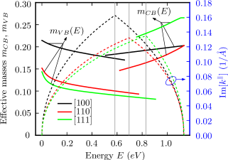
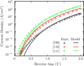
We now test our model against experimental data Solomon et al. (2009) available for BTBT in silicon. This data is unique in that the same doping profile has been used to study BTBT along the , and directions. We implement our model in the open source drift-diffusion based TCAD code pyEDA Chen . We also modify the pyEDA code to include the effects of degenerate doping and incomplete ionization of dopants. Information regarding the phonon energies, modes and electron-phonon deformation potentials are taken from Ref. Fischetti et al., 2007. Owing to the conservation condition in eq. (8), we only require the phonon modes along the direction in silicon. To summarize, there is one longitudinal optical (LO) and acoustic (LA) mode, and two doubly degenerate transverse optical (TO) and acoustic (TA) phonon modes with energies , , , and deformation potentials , , , respectively. The density is taken from Ref. Tanaka, 1995. The TA mode provides the largest contribution to the BTBT current (for example, of the total current at reverse bias of for the direction in the device considered here.) In order to simplify computation, we restrict ourselves to the tunneling paths (and hence values of ) that minimize the area bounded by the imaginary parts of the valence and conduction bands involved in tunneling. Other tunneling paths enclose much larger areas and are hence expected to contribute negligibly to tunneling current, due to the term in eq. (8). Further, these paths all happen to originate from the valence band for light holes. The multiplicity for transport along the , and directions respectively (Appendix C) in silicon. Fig. 2 shows the energy dependent effective mass computed using an tight binding scheme Ajoy et al. (2011) and parameters from Ref. Boykin, Klimeck, and Oyafuso, 2004. The invariant product is , written using a coordinate system aligned with the major and minor axes of any one of the six conduction band ellipsoids. Similarly, the product is , corresponding to the effective masses of the light holes , and along the three orthogonal , and directions respectively. The value of and in eq. (8) are obtained from these invariant products and the values of , in Fig. 2 at the band edges. Fig. 3 shows that the results of our model agree very well with the experimental data. We have assumed a bandgap , corresponding to a bandgap narrowing of , by fitting the results of our model with the experimental data (We found this to be a better strategy than calculating the bandgap narrowing apriori, since the value of bandgap narrowing is dependent on doping, which is non-uniform for the devices we have considered here. The model for BTBT that we have derived assumes a uniform bandgap.) This value of narrowing is consistent with studies on bandgap narrowing in space charge regions Chen, Li, and Teng (1989); Lowney (1985) for the doping levels considered here. Further, based on a result obtained using theory Miller (2008) that , we have scaled all the effective masses by the factor , where is the bandgap for moderate doping. At low values of reverse bias, our model underestimates the experimentally observed value of current (for e.g., for transport along , at , whereas ). It is likely that some other mechanism of current transport (such as tunneling via traps, or SRH recombination via traps) could possibly explain the difference between our simulations and experimental data at small values of reverse bias (see for e.g. Fig. 7 of Ref. Schenk, 1993). It is possible that the trap distribution/energies are different in the experimental samples that we have compared our model against for transport along the different directions, leading to a better match between the experimental data and the model for the direction. A detailed analysis of this deviation could be the focus of future work.
IV Error due to parabolic approximation of complex bands
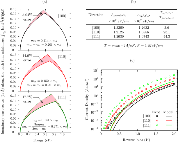
We now demonstrate the inadequacy of using a parabolic approximation to the complex bandstructure while computing BTBT currents. Fig. 4(a) shows a parabolic approximation (dashed lines) to the complex bands (solid lines, obtained from an calculation) along the tunneling path that minimizes . The curvatures of the imaginary and real bands are identical at the band extrema. The values of , and are from Ref. Boykin, Klimeck, and Oyafuso, 2004. The expressions for are from Ref. Pandey et al., 2010, based on the theory in Ref. Rahman, Lundstrom, and Ghosh, 2005. The areas in the method and parabolic approximations are listed in Fig. 4(b); the errors due to a parabolic approximation with respect to the results are indicated in Fig. 4(a). Note that the error is largest along the direction. A simple result for the transmission (setting the phonon energy to , assuming a uniform field , and using a WKB approximation) gives Laux (2009) , where is the multiplicity of tunneling paths. As indicated in Fig. 4(b), the parabolic approximation underestimates the tunneling current by a factor of along the direction. Finally, Fig. 4(c) shows the results of using the parabolic approximation in our BTBT model (as usual, is computed using transfer matrices). We use the same bandgap (and scaling of masses) as in Fig. 3. Clearly, the parabolic approximation does not capture the measured data. Further, it significantly underestimates the difference between the currents in the and directions. We would like to clarify that though the choice of effective energy gap can increase or decrease the absolute values of the current levels, it cannot correctly predict the difference in currents between the and directions. This can been seen from Fig. 4(a), where error in the action for tunneling along the direction is significantly greater than that along the direction.
V Conclusion
In conclusion, we have presented a multiscale model for phonon assisted BTBT that accounts for the complex bandstructure within the bandgap of an indirect semiconductor. We have shown that the predictions of this model compare very well with experimental data for BTBT in silicon along different orientations. We have shown that including the effect of non-parabolic complex bands is important to capture the correct difference between tunneling currents observed along the , and directions. The framework presented here can be used to modify Tanaka’s results Tanaka (1994) on BTBT across a direct bandgap to include the effect of an energy dependent effective mass. Such an extension will find application in treating BTBT in materials such as germanium, where the direct bandgap is only about larger than the indirect bandgap.
Appendix A Description of wavefunctions and energies
| Region | Wavefunction | Energy | |
|---|---|---|---|
| VB | |||
| — eq. (1) | |||
| CB | |||
| — eq. (1) | |||
The wavefunctions within the effective mass approximation are written as and for an electron in the valence and conduction bands respectively. The extents of the device in the directions are . As shown in Fig. 1, the component of the energy of an electron corresponding to its motion in the plane is designated in the valence band and in the conduction band. Note that
Further, following Ref. Tanaka, 1994, , and , are plane waves. On the other hand, and are assumed to be plane waves outside the classical turning points (i.e. and ). This corresponds to making the approximation (see Fig. 1(b) of Ref. Tanaka, 1994) that the energy bands are flat until (with the valence band edge at ) and beyond (with the conduction band edge at ). Table 1 summarizes the expressions for the wavefunctions and energies in different regions.

Appendix B Derivation of tunneling current
The summations in eq. (7) are first converted into integrals, for e.g. , . Further, the integrals are rewritten in terms of energies using the relationship between and outside the region of tunneling, for e.g. , . In order to determine the limits of integration, we impose the conditions that and . By definition, . Anticipating the physical reality that tunneling will be dominated by states with , we also impose conditions that and . This gives the limits of integration. The current density is
| (1) | ||||
where the summation over has also been converted to an integral. is eliminated from eq. (1) due to the delta function. Further simplification requires making the assumption that only states with small values of , and hence contribute significantly to tunneling. Tanaka Tanaka (1994) approximates an integral of the form where (and , ) for the case that is significant only for small . However, Tanaka’s expressions do not include the Fermi functions as in eq. (1). We drop in the arguments of the Fermi functions and write
| (2) | ||||
Finally, following Ref. Tanaka, 1994, and hence are functions of . We expect that the dominant contribution to tunneling will be for , . We thus expand using a Taylor approximation
| (3) |
To determine the coefficients in the above equation, we make the approximation that , are gently varying functions of , and hence ignore their spatial derivatives. This allows reuse of many of the expressions derived in Ref. Tanaka, 1994 with minor modifications. Then is a solution of the equation
| (4a) | ||||
| and represents the point of intersection of the imaginary parts of the complex valence and conduction bands. We have | ||||
| (4b) | ||||
| which gives eq. (9a). The coefficient is purely imaginary and hence can be ignored. Further, | ||||
| (4c) | ||||
| where is a reduced mass given by | ||||
| (4d) | ||||
| Also, | ||||
| (4e) | ||||
| and | ||||
| (4f) | ||||
Finally, from eqs. (2), (3), (4a) - (4f), we get eq. (8). Note that the Gaussian integral over converts the condition into the condition since by the method of steepest descent.
Appendix C Multiplicity of tunneling paths
The conduction band minima in silicon are along the six equivalent directions. As described in Ref. Ajoy et al., 2011, the positions of these valleys are used to determine the values of to compute the complex bands . The value represents the magnitude of the component of the wavevector, parallel or antiparallel to the transport direction, oriented along the direction of an arrow through the valley corresponding to , as shown in Fig. 5. Paths having the same are shown in the same color. Further, the paths shown solid in red have complex bands that enclose a smaller area bounded by the imaginary parts of the valence and conduction bands than those shown dashed in blue. It is necessary to consider valleys that lie on both sides of the plane (shown shaded). Fig. 5 gives the multiplicity for the , and directions.
Appendix D Transfer Matrix Method as an improvement over the WKB approximation
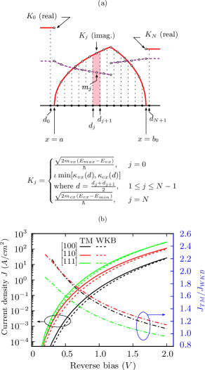
In order to use the transfer matrix method, we define points , as shown in Fig. 6(a), so that the values of the wavevector are available at the midpoints of intervals , . There are interfaces between the classical turning points and . For each of these interfaces, we have Pandey et al. (2010) a transfer matrix , given by
| (1) |
with and . is defined in Fig. 6(a); is similarly evaluated from or , based on whether the wavevector corresponds to the valence or conduction bands respectively. Note that for the situation , described in eq. (3). The transmission is then
| (2a) | ||||
| (2b) | ||||
Also note that and based on the assumption that the energy bands are flat outside the classical turning points.
Acknowledgment
A. Ajoy wishes to thank IBM India for financial support. The authors wish to thank Dr. Rajan Pandey (IBM Bangalore) and G. Vijayakumar (IIT Madras) for useful discussions.
References
- Rivas et al. (2001) C. Rivas, R. Lake, G. Klimeck, W. Frensley, M. Fischetti, P. Thompson, S. Rommel, and P. Berger, Appl. Phys. Lett. 78, 814 (2001).
- Luisier and Klimeck (2010) M. Luisier and G. Klimeck, J.Appl. Phys. 107, 084507 (2010).
- Luisier and Klimeck (2008) M. Luisier and G. Klimeck, in International Conference on High Performance Computing, Networking, Storage and Analysis (IEEE, 2008) pp. 1–10.
- Luisier and Klimeck (2009) M. Luisier and G. Klimeck, Phys. Rev. B 80, 155430 (2009).
- Luisier et al. (2006) M. Luisier, A. Schenk, W. Fichtner, and G. Klimeck, Phys. Rev. B 74, 205323 (2006).
- Hurkx (1992) G. A. M. Hurkx, IEEE Trans. Electron Devices 39, 331 (1992).
- Pandey et al. (2010) R. K. Pandey, K. V. R. M. Murali, S. S. Furkay, P. J. Oldiges, and E. J. Nowak, IEEE Trans. Electron. Devices, 57, 2098 (2010).
- Kao et al. (2012) K.-H. Kao, A. S. Verhulst, W. G. Vandenberghe, B. Soree, G. Groeseneken, and K. De Meyer, IEEE Trans. Electron Devices 59, 292 (2012).
- Kane (1961) E. Kane, J. Appl. Phys. 32, 83 (1961).
- Tanaka (1994) S. Tanaka, Solid State Electron. 37, 1543 (1994).
- Vandenberghe et al. (2011) W. Vandenberghe, B. Sorée, W. Magnus, and M. Fischetti, J. Appl. Phys. 109, 124503 (2011).
- Schenk (1993) A. Schenk, Solid State Electron. 36, 19 (1993).
- Keldysh (1958) L. Keldysh, Soviet Journal of Experimental and Theoretical Physics 6, 763 (1958).
- Kohn (1959) W. Kohn, Phys. Rev. 115, 809 (1959).
- Heine (1963) V. Heine, Proceedings of the Physical Society 81, 300 (1963).
- Laux (2009) S. Laux, in International Workshop on Computational Electronics (IEEE, 2009) pp. 1–2.
- Tsu and Esaki (1973) R. Tsu and L. Esaki, Appl. Phys. Lett. 22, 562 (1973).
- Solomon et al. (2009) P. Solomon, S. Laux, L. Shi, J. Cai, and W. Haensch, in Device Research Conference 2009 (IEEE, 2009) pp. 263–264.
- (19) S. E. Laux and P. M. Solomon, Unpublished .
- Geller and Kohn (1993) M. Geller and W. Kohn, Phys. Rev. Lett. 70, 3103 (1993).
- Huang et al. (2008) C. Huang, S. Chao, D. Hang, and Y. Lee, Chin. J. Phys. 46 (2008).
- Ajoy et al. (2011) A. Ajoy, K. V. R. M. Murali, S. Karmalkar, and S. E. Laux, in Device Research Conference, 2011 (IEEE, 2011) pp. 113–114.
- Ajoy, Murali, and Karmalkar (2012) A. Ajoy, K. V. R. M. Murali, and S. Karmalkar, J. Phys.: Condens. Matter 24, 055504 (2012).
- Rahman, Lundstrom, and Ghosh (2005) A. Rahman, M. S. Lundstrom, and A. W. Ghosh, J. Appl. Phys. 97, 053702 (2005).
- Tanaka (1995) S. Tanaka, Solid State Electron. 38, 683 (1995).
- Vandenberghe et al. (2010) W. Vandenberghe, B. Sorée, W. Magnus, and G. Groeseneken, J. Appl. Phys. 107, 054520 (2010).
- Mayer (2010) A. Mayer, Journal of Physics: Condensed Matter 22, 175007 (2010).
- (28) S. Chen, URL: http://github.com/cogenda/pyEDA .
- Fischetti et al. (2007) M. Fischetti, T. O’Regan, S. Narayanan, C. Sachs, S. Jin, J. Kim, and Y. Zhang, IEEE Trans. Electon. Devices 54, 2116 (2007).
- Boykin, Klimeck, and Oyafuso (2004) T. B. Boykin, G. Klimeck, and F. Oyafuso, Phys. Rev. B 69, 115201 (2004).
- Chen, Li, and Teng (1989) H. C. Chen, S. S. Li, and K. W. Teng, Solid State Electron. 32, 339 (1989).
- Lowney (1985) J. Lowney, Solid State Electron. 28, 187 (1985).
- Miller (2008) D. Miller, “Quantum Mechanics for Scientists and Engineers,” (Cambridge University Press, 2008) Chap. 8, pp. 230–33.