Spectral Brilliance of Channeling Radiation at the ASTA Photoinjector
Abstract
We study channeling radiation from electron beams with energies under 100 MeV. We introduce a phenomenological model of dechanneling, correct non-radiative transition rates from thermal scattering, and discuss in detail the population dynamics in low order bound states. These are used to revisit the X-ray properties measured at the ELBE facility in Forschungszentrum Dresden-Rosenstock (FZDR), extract parameters for dechanneling states, and obtain satisfactory agreement with measured photon yields. The importance of rechanneling phenomena in thick crystals is emphasized. The model is then used to calculate the expected X-ray energies, linewidths and brilliance for forthcoming channeling radiation experiments at Fermilab’s ASTA photoinjector.
1 Introduction
Channeling radiation offers the promise of a quasi-monochromatic and tunable X-ray source with electron beams of moderate energies (tens of MeV) passing through a thin crystal. This radiation has been experimentally observed at several laboratories and many of the experimental features are well understood from theoretical considerations. Reviews can be found in several publications, see e.g. Refs. [1, 2, 3].
Channeling and channeling radiation experiments have a long history at Fermilab, see e.g. Ref. [4]. Those were carried out at the A0 photoinjector which had a maximum beam energy of about 15 MeV. A new photoinjector ASTA is being commissioned at Fermilab, which will use an L-band (1.3 GHz) linac to generate beams with energies initially in the range 20-50 MeV and later to 300 MeV and higher with the addition of one or more ILC style cryomodules [5]. Channeling radiation experiments with beams in the lower energy range have been planned and descriptions of the planned experiments can be found in Refs. [6, 7]. The goal is to generate X-ray beams with high average brilliance using low emittance electron beams with the aim of increasing the brilliance by about six orders of magnitude over that obtained with channeling experiments conducted at FZDR’s ELBE linac [8]. Once demonstrated, compact X-ray sources from channeling radiation can be designed and built with X-band linacs.
In this report we revisit the theoretical model for channeling radiation with the aim of improving the calculation of the X-ray intensity. We compare the calculations of the revised model with the measurements of previous experiments at ELBE and find better agreement of the photon yields with the experimental values shown in ref. [9]. We then use this model to calculate the expected photon yields and X-ray brilliance at ASTA.
2 Theoretical model
In the case of planar channeling, the particle motion in its rest frame can be well approximated by motion in a single transverse direction (here ) orthogonal to the plane. For particle energies below 100 MeV, the X-ray energy spectrum is discrete and the radiation is best understood as emitted during transitions between the discrete bound states in the crystal potential and requires a quantum mechanical treatment. The Schroedinger equation for the electron wave function in the particle rest frame is
| (1) |
Here is the usual kinematic factor related to the velocity and is the one dimensional continuum potential obtained by averaging the three dimensional atomic potential along the orthogonal directions . Taking into account the lattice periodicity, the potential can be expanded as a Fourier series
| (2) |
Here is the lattice spacing in reciprocal space while is the lattice spacing in direct space. The Fourier coefficients are typically obtained from expanding the electron form factor (defined in Eq.(14)) into a sum of four Gaussians with four Doyle-Turner coefficients [10]. We use here instead six coefficients as used in Ref. [11] which extends the range of validity of the approximation from Å-1 to Å-1 for planar channeling.
| (3) |
Here is the reciprocal lattice vector, is the volume of the unit cell, is the Bohr radius, are the coordinates of the th atom in the unit cell and is the Debye-Waller factor describing thermal vibrations with mean squared amplitude , assumed to be the same for all atoms.
The wave function solution for the periodic potential is given in terms of Bloch waves
| (4) |
where is the electron wave number. In practice, the Fourier expansion for the potential and the wave function is limited to a finite number of modes , in the cases considered here . Substitution of Eqs. (2) and (4) into the Schroedinger equation reduces it to an eigenvalue problem with a matrix whose components are [12]
| (5) |
Solutions to the eigenvalue problem results in the eigen-energies and the coefficients determining the wavefunctions .
2.1 Radiative transitions
Radiative transitions from one state to another lead to photon emission and the transition rates are given by Fermi’s golden rule which states that the transition rate per unit solid angle, per length of traversal into the crystal and per unit photon energy is proportional to the matrix element of the transition operator between the states, i.e.
| (6) |
where corresponds to the dipole operator and is the probability of occupation in the state at a distance into the crystal.
Applying this rule yields the differential energy angular spectrum from a state to state as [13, 14, 15, 12]
| (7) | |||||
where is the fine structure constant, is the Compton wavelength of the electron, are the energies of the states respectively, is the crystal thickness, is the energy dependent photon absorption coefficient, is the X-ray energy at the angle of observation, is the X-ray energy at zero angle, where is the multiple scattering angle during channeling and is the total linewidth of the transition line. From this the differential angular spectrum is found from
| (8) |
where the integration is done over the linewidth of the spectral line with its peak at . These transitions only occur between states of opposite parity because the dipole transition matrix element is non-zero only between these states. The dipole operator is of odd-parity and the bound states in planar channeling are states of definite parity: even parity for n even and odd for n odd.
With the wave function defined in terms of the Fourier coefficients , the dipole matrix elements between two states is given by
| (9) |
where is the inter-planar distance and are the coefficients in the Bloch wave expansion (see Eq.(4)) of respectively.
If the eigen-energies of the two states involved in the transition are , the energy of a photon emitted at zero angle and emitted at angle with the beam direction are given by
| (10) |
2.2 Non-Radiative transitions
In addition to the radiative transitions, electrons can also change energy by non-radiative transitions which we discuss here. Electrons in the lower bound states are closer to the atomic nuclei and can change energy due to thermal scattering with the vibrational motion of the atoms. This energy exchange can lead to a change of the wave vectors within the same Brillouin zone (intra-band scattering) or even transfer them to different energy states (inter-band scattering). This electron-phonon scattering is the dominant contribution to the non-radiative transitions that change the populations of the states; a relatively smaller contribution is played by the electron scattering off atomic electrons. The transition probability due to thermal scattering that an electron will move from state with momentum to state with a different momentum is given by a transition rate per unit length where
| (11) |
where the potential describes the inelastic scattering. It is the imaginary part of a complex potential with the real part being the continuum potential which describes the elastic scattering. Intra-band scattering is described by while inter-band scattering has . Calculation shows that the variation of the rate within an energy band (Brillouin zone) is smaller than the variation between bands. For clarity of notation, we will drop the momentum indices from in the following but they are understood to be present.
Similar to the real potential, the imaginary potential can also be expanded in a Fourier series as
| (12) |
where is the unit reciprocal lattice vector.
We briefly summarize the procedure for calculating the imaginary potential and hence the Fourier coefficients , following the method in Ref. [11]. As is done in solving for the energy eigenvalues, the incident and scattered wave functions of the electron are represented as sums of Bloch functions with the sums extending over many reciprocal lattice planes. In general thermal scattering occurs in all three directions, hence a three dimensional formalism is necessary. The incident and scattered wave functions can be written as
| (13) |
Here are the coefficients in the expansion, the sum over extends over reciprocal lattice planes, are the reciprocal lattice vectors while the sum over extends over the atoms in the crystal. are the incident and outgoing wave vectors of the electron and . is the electron scattering form factor given by
| (14) |
Here is the real part of the atomic potential.
The transition rate is found from the intensity of the thermally diffuse scattering
| (15) |
where is the solid angle into which the particle is scattered, is the volume of the crystal. The diffuse scattering intensity is related to the total scattering intensity via
| (16) |
Here is the Bragg scattering or the coherent scattering intensity. Bragg scattering does not generally lead to energy exchange between electrons and the atoms but instead modulates the amplitude of the electron intensity in the crystal [16]. It occurs even when the atoms are stationary, so the diffuse inelastic scattering intensity is found by extracting only the contribution from the thermally induced vibrations.
In evaluating the scattered intensity, the instantaneous position can be represented as where is the stationary equilibrium position of the th atom while represents the time dependent position due to thermal vibrations. Then a thermal averaging is performed assuming that the thermal vibrations are isotropic. The terms in the total scattered intensity that are independent of the atomic coordinates define the incoherent thermally diffuse scattering
| (17) | |||||
Here represents the thermal average, , and is the number of atoms in the crystal. This incoherent intensity would vanish in the absence of thermal vibrations.
Equating the two expressions for the transition rates in Eq.(11) and Eq.(15) leads to an expression for the Fourier coefficients
| (18) | |||||
The element of solid angle in this integral is written as . The second equality follows from , hence when . Using the Doyle-Turner like expansions.for the real potential, the electronic form factors can be written as
| (19) |
where
Performing the integrations, the expression for the Fourier coefficients of the imaginary potential is
Again, we note that the coefficients vanish in the absence of thermal vibrations . This potential depends on the particle energy only through , hence this potential is nearly independent of particle energy for relativistic electrons. This expression differs from the incorrect expression (Eq.(A20)) in Ref. [11]. The resulting imaginary potential turns out to have a smaller magnitude and the opposite sign to the imaginary potential used in the numerical modeling for the ELBE experiments, e.g Eq.(11) in reference [12].
From the numerical calculations, the transition rates are found to obey the approximate selection rule that only same parity transitions are allowed, i.e. . The odd parity transitions are non-zero but small.
The probability of a state changes as the electron propagates through the crystal. The rate of change is determined by the transition rates as
| (21) |
where is the transition probability from a state to state . The first term in the sum corresponds to entering the state from other states while the second term corresponds to electrons leaving that state. In this model, equilibrium populations, i.e. are reached when the populations in all states are equal .
2.3 Dechanneling
If the electron is scattered into a free state, it is possible that the electron will remain in a free state and not be scattered back into a bound state while propagating through the crystal. In addition, multiple scattering can move electrons from lower states to higher states and effectively remove electrons from contributing to the radiation yield. This enhanced dechanneling can be taken into account phenomenologically in the above model by removing those electrons scattered into free state above a certain energy from contributing to the photon yield. Thus the above equation would be modified to a set of two equations. If denotes the free state at which electrons are dechanneled and do not scatter back into the bound states, then the propagation of the probabilities are given by
| (22) | |||||
| (23) |
The first term in Eq (22) restricts the electrons entering state to only those from states below while the second term allows the escape of electrons from this state to all states. Similarly for states at and above , electrons can enter from all states (1st term in Eq.(23)) but can only escape to states above . These set of equations conserve population, i.e. , as they should. In this model there are no equilibrium solutions except for those states which are depopulated at the beginning of the crystal and remain so. For the other states, the asymptotic solutions in this model at large are given by for and for .
A complete theory would have transition rates from multiple scattering in the model, but in its absence we will use experimental data to find the best value for . In the cases we will consider, is found to be determined primarily by the crystal thickness and not by the electron energy. We expect that will increase with crystal thickness to reflect the higher rechanneling probability that electrons will scatter into bound states with increasing thickness. This was observed to be the case in experiments at the Darmstadt linac [15] and our fits to the experimental data from the ELBE linac will also show this to be the case.
A proper treatment of dechanneling at low energies using a quantum mechanical treatment still seems to be lacking. However, when the electron energy is high enough that channeling radiation can be treated classically, then a Fokker-Planck treatment of the diffusive motion has been used to describe dechanneling. Results from one such analysis and comparison with experiments using 855 MeV electrons were reported in Ref. [17]. A brief survey of dechanneling phenomena at high energies for negatively and positively charged particles was reported in Ref. [18].
2.4 Line width and length scales
The finite lifetime of quantum states, Bloch wave broadening of each energy band due to the variation of transverse momenta, and multiple scattering are the dominant sources of line broadening in the regime of our interest. Other less significant sources are the Doppler broadening due to emission at non-zero angles, electron beam energy spread and detector resolution. Here we will consider the dominant effects and the length scales associated with line broadening effects, more complete discussions can be found in Refs. [11, 12].
Coherence length: This is a measure of the length over which a radiating electron stays in phase and it determines the lifetime of the bound states. Thermal (phonon) scattering, atomic electron (plasmon) scattering and other incoherent scattering effects change the phase of the initial wave function of the electrons and they lose coherence. These scattering effects can be described by the imaginary potential discussed above. The coherence length for transitions between two states is given by
| (24) |
where is the expectation value of the imaginary part of the complex potential in the state . The line width due to this finite lifetime of each state is given by
| (25) |
The correction to the imaginary potential discussed in the previous section makes it smaller and hence the calculated coherence lengths are larger than those reported in Ref. [12].
Bloch wave broadening: Each energy band has a finite width due to the spread of wave vectors within each Brillouin zone. Hence the energy spread from transitions between states and is given by
| (26) |
where is the reciprocal lattice spacing and is the transverse component (here ) of the wave vector. The width is larger for the higher bound states because of their larger range of transverse momentum. The relative importance of Bloch wave broadening increases with energy as the number of bound states increases.
Multiple scattering of channeled particles: This contributes to the line width by changing the angle of the scattered electron and hence the angle at which photons are emitted and their energy. For particle scattering in an amorphous medium, the rms scattering angle is given by [19]
| (27) |
where is the thickness and is the radiation length, the length over which an electron loses of its initial energy. This expression is considered to be accurate to about 10% for thickness down to 0.001 [19]. Experimental estimates show that the scattering angle of channeled particles in a crystal is less than that in an amorphous medium. Estimates of the scaling between the rms multiple scattering angles during channeling and in an amorphous crystal are in the range [11, 12]. The range of values in the numerical coefficient depends on the crystal thickness, smaller values for larger thickness, but is nearly independent of the beam energy.
The change in the angle of emission Doppler shifts the photon energy, with its energy given by the second equation in Eq.(10). The mean photon energy is found by averaging the angle dependent energy over the distribution of multiple scattering angles, assumed to be Gaussian. Thus
| (28) |
while the rms width of this distribution may be taken as a measure of the linewidth due to multiple scattering,
| (29) |
Dechanneling length or Occupation length: A simple estimate of the length over which particles dechannel due to multiple scattering is given by setting the rms multiple scattering angle equal to the Lindhard critical angle yields [20]
| (30) |
where is the depth of the atomic potential, is the particle energy. This is based on a strictly classical approach and predicts that the dechanneling length increases linearly with energy. Measurements however have shown that the dechanneling lengths for electrons with energies in the tens of MeV are higher than the above simple estimate and do not scale linearly with energy [14].
Quantum mechanically, a similar idea is expressed by the concept of an occupation length which is the length over which the initial probability in a quantum state falls by a factor , i.e.
| (31) |
This occupation length depends on the states involved in the transition, the plane of channeling and on the beam energy. It was measured in a few experiments, e.g. Refs. [14, 21] with beam energies in the 5 - 54 MeV range. Some measured values for the (1 0) transition in the (110) plane are shown in Table 1.
Photon formation length: In the simplest version, this length represents the length scale over which the photon “shakes free” from the electron after formation and separates from it by a reduced wavelength [3]. It is given by
| (32) |
where is the photon frequency. Clearly the crystal thickness should be larger than this formation length for a significant photon yield.
Photon absorption length: The photon absorption length within a material is given by
| (33) |
where is the atomic density, is the atomic number and is the total cross-section of all processes that lead to photon absorption during its passage through the material. These include the photo-electric effect, Compton scattering, and also pair production for photon energies sufficiently above 1 MeV. The scattering cross-sections for these processes are well known and the absorption lengths at different photon energies can be obtained from tables maintained by NIST [22].
Table 1 shows the values of these length scales for some representative electron and photon energies.
| Photon lengths | ||||
| [keV] | Length | [keV] | Length | |
| Formation length with 50 MeV e- | 10 | 0.38[m] | 80 | 0.047[m] |
| Photon absorption length | 10 | 1.26 [mm] | 80 | 17.7 [mm] |
| Electron lengths | ||||
| [MeV] | Length | [MeV] | Length | |
| Electron radiation length | 20 | 16.7 [cm] | 50 | 14.9 [cm] |
| Dechanneling length | 20 | 0.71 [m] | 50 | 1.58 [m] |
| Occupation length (1 0) | 17 | 20 [m] | 54 | 36[m] |
The crystal thickness should be large enough for enough photons to be emitted from the particle, so but small enough that most photons do not get absorbed within the crystal, i.e. . Since in all cases of interest , the radiation length, the electron will lose very little of its energy through its passage through the crystal. We also note that the classical dechanneling length found from the simple estimate in Eq (30) significantly underestimates the occupation length found from measurements at nearby energies.
3 Simulations of ELBE experiments
We used a Mathematica notebook developed for modeling the channeling radiation experiments at the ELBE facility [23]. This notebook (called PCR) or some version of it was used to model the ELBE experiments and results in Ref. [9] showed the line widths were about half the measured values and photon yields were about a factor of two higher than the experimental results. However tests with the notebook available from the source [23] showed much greater discrepancies with the ELBE experimental results. We therefore corrected and added features to the notebook, the more significant changes are listed here in order of importance:
-
1.
Used the set of equations (23) to model the effects of enhanced dechanneling due to multiple scattering and other scattering phenomena from the bound and quasi-free states.
-
2.
Corrected the imaginary part of the potential as described in Section 2.2. This also included correcting the matrix elements of the imaginary part of the potential. These matrix elements now better obey the approximate selection rule that the non-radiative transitions occur primarily between states of the same parity. The Fourier coefficients of the real and imaginary parts of the potential are now also calculated in the notebook.
-
3.
Included the effects of a finite beam divergence.
-
4.
Included the contributions to the linewidth from Bloch-wave broadening and multiple scattering to the total line width. The notebook in Ref. [23] contained only the contribution from the coherence length.
-
5.
Corrected the line shape in the intensity spectrum calculation
-
6.
Included photon self-absorption within the crystal.
Further improvements could be made to the physics model. These include:
- •
-
•
The rms multiple scattering angle while channeling in a crystal is obtained from that in an amorphous medium by a scaling factor, based on limited experimental data. This could be replaced by a calculation of the multiple scattering angle during channeling from first principles.
Table 2 shows the main parameters of the ELBE facility which we used in the simulations reported here.
| Crystal thickness[m] | 42.5, 168, 500 |
| Beam energy [MeV] | 14.6, 17, 30, 34 |
| Uncertainty in beam energy [MeV] | 0.2 |
| Transverse norm. emittance [mm-mrad] | 3. |
| Beam divergence, both planes [mrad] | 0.1 |
| Relative energy spread | |
| Beam size at crystal [mm] | |
| Average beam current [nA] |
First we discuss the coherence length calculation. Since the corrected imaginary part of the potential is weaker that that used in the previous calculations for ELBE, the coherence length found here is longer and hence the linewidth from this effect is smaller than that reported in Ref. [12]. We note that this coherence length includes only the effect of inelastic thermal scattering and does not include the effects of inelastic electron scattering. Table 3 lists the coherence length from thermal scattering at the ELBE energies for some low order transitions
| Beam energy [MeV] | [m] | [m] | [m] |
|---|---|---|---|
| 14.6 | 1.87 | 4.08 | 5.98 |
| 17.0 | 1.79 | 3.75 | 5.95 |
| 25.0 | 1.62 | 3.01 | 5.24 |
| 30.0 | 1.55 | 2.74 | 4.70 |
The coherence length for the transition extracted from measured data [12] was about 0.65 m, more than a factor of two smaller than the calculated values. This discrepancy is most likely due to neglecting the inelastic electron-plasmon and electron-core electrons from the atom scattering.
3.1 Population dynamics
The populations in the states change as the electron moves through the crystal. In our simulations we have modeled dechanneling due to all effects in a heuristic fashion using the model with the free parameter in Eqs. (22) and (23). Let denote the index of the highest bound state at a given energy; at 14.6 MeV and at 30 MeV with the ground state index . For each energy and crystal thickness, the appropriate values of were determined by comparing with the measured photon yield, to be discussed below in Section 3.2. Lower values of imply dechanneling from more free states and hence lower photon yields.
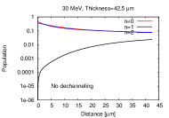
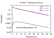
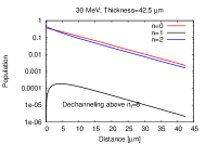
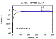
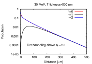
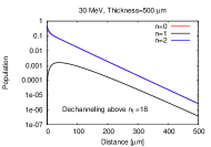
Here we discuss the probabilities found from the numerical solutions of Eqs. (22), (23). Figures 2 and 2 show the populations as a function of the distance into the crystal for thicknesses of 42.5 m and 500 m respectively at the beam energy of 30 MeV. Only the three lowest bound states are shown in each case. The appropriate values of change with the thickness. The left plot in both figures show the populations without enhanced dechanneling (). Without the additional dechanneling, the populations in the three states equalize and reach equilibrium at around 200 m, as seen in Fig. 2. This length is relatively insensitive to the energy, being about the same at all energies modeled. Without dechanneling from multiple scattering, the photon yield was significantly higher than the experimental value.
Two values of were chosen such that the measured yield lay in between the calculated photon yields with these values of . At 42.5 m thickness, these values at 30 MeV were while at 500 m, these were . The middle plot in Figures 2 and 2 shows the populations with the higher values of in each case. As expected, the populations in these states do not reach equilibrium but continue to decrease with distance. At 500 microns, the three states have nearly equal populations and fall at the same rate implying that the occupation lengths are about the same in these states. The right plot in both figures shows the populations when is set so that the calculated yield is a slight under-estimate of the measured yield. For both thicknesses, we find that the populations in the state increase by several orders of magnitude before reaching a maximum and falling at the same rate as in the even bound states. We find that if is so low that the initial increase in the state is less than an order of magnitude, the dechanneling is too strong and the photon yield is much lower than the measured value. The dependence of for different values of is similar at other energies.
Fits to the population in the lowest order even states
show good fits to an exponential form
, especially at the lower energies. At
30 MeV, a better fit is obtained with a sum of two exponentials of the
form , where
. However the weight of the second term is small,
typically .
Since the intensity of the transition is determined by the
population in the state, we consider it in a little more detail.
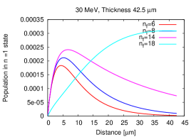
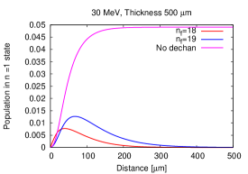
Figure 3 shows the populations in this state
at 30 MeV and different thicknesses at a few chosen values of the
parameter . For both thicknesses we observe that as decreases,
the distance at which the population reaches a maximum decreases and also
decays at a faster rate, i.e. with a shorter occupation length.
The behavior shown can be modeled by a functional form
| (34) |
Here is a length parameter determined by the maximum of the population while the distance at which the population is maximum is given by . Table 4 shows fitted values of and at different beam energies and different thicknesses. The fits for the occupation length in the bound states yield very similar values to those shown in this table.
| Energy | Thickness | Occ. length [m] | ||
|---|---|---|---|---|
| 14.6 | 42.5 | 4 | 8.6 | 0.93 |
| 14.6 | 500 | 16 | 39.5 | 0.19 |
| 30.0 | 42.5 | 6 | 8.2 | 0.54 |
| 30.0 | 500 | 18 | 52.7 | 0.75 |
We observe that the occupation length changes relatively little with energy but depends strongly on the thickness. This is one indication that the rechanneling probability which increases with thickness has a strong impact on the population dynamics. Rechanneling occurs when an electron in a dechanneled free state enters a bound state by losing transverse energy due to a number of processes including multiple scattering. It is possible that the rechanneling probability and the occupation length saturate for sufficiently thick crystals. Nevertheless from the results in Table 4 we can conclude that occupation lengths cannot be considered in isolation from rechanneling and crystal thickness and that classical expressions for the dechanneling length such as in Eq. (30) may be invalid in the quantum regime.
Equation (34) can be used to estimate the crystal thickness at which the intensity of the transition will saturate. The intensity for a crystal of thickness relative to an infinitesimally thin crystal in the limit that the photon absorption length is long compared to the crystal thickness is proportional to the integral of ,
| (35) |
where is the gamma function.
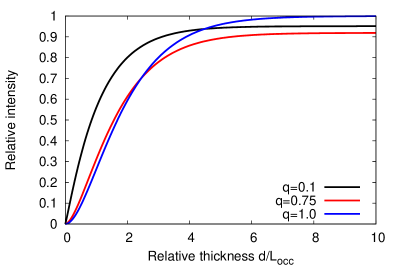
Figure 4 shows the relative intensity as a function of the relative crystal thickness for three values of the power law exponent . Figure 4 shows that the intensity of the transition saturates within a thickness of for the range of values considered. This suggest that when m as seen in Table 4, crystal thickness of m may suffice to optimize the channeled fraction and the intensity of the transition.
3.2 X-ray energies, line widths and photon yields
Here we discuss the main aspects of the X-ray photon spectrum for the ELBE parameters. We have assumed here and in subsequent calculations that variations in the incidence angle from zero are small compared to the beam divergence. Table 5 shows the energies of the 1 0 transition for different beam energies and different crystal thicknesses.
| Energy | Thickness | Energy[keV] | Linewidth [keV] | ||
|---|---|---|---|---|---|
| [MeV] | m | ||||
| 14.6 | 42.5 | 16.58 | 16.35 | 1.43 | 0.74 |
| 168 | 16.99 | 16.01 | 1.74 | 1.09 | |
| 500 | 16.47 | 15.63 | 2.15 | 1.49 | |
| 17 | 42.5 | 21.72 | 21.41 | 1.94 | 0.92 |
| 168 | 22.37 | 20.97 | 2.35 | 1.40 | |
| 500 | 21.38 | 20.48 | 2.73 | 1.92 | |
| 25 | 42.5 | - | 42.02 | - | 1.78 |
| 30 | 42.5 | 56.19 | 57.58 | 5.85 | 2.46 |
| 168 | 56.22 | 56.44 | 6.09 | 3.72 | |
| 500 | 55.06 | 55.13 | 11.96 | 5.09 | |
In order to mimic the experimentally observed dependence of the X-ray energy on the thickness, we have used , the average value of the peak due to Doppler shift from multiple scattering, given in Eq(28). Due to the greater multiple scattering in thicker crystals, the value of decreases with thickness. This trend is also observed in the experimental values when going from 42.5 to 500 m at all energies but for 168 m only at one energy. In most cases, the simulated value agrees to within 6% which is well within the error bars on the measurements.
In comparing the linewidths, we have defined the quantity as the experimental line width but with the detector energy resolution removed via a quadrature, i.e. where is the measured linewidth. Table 5 shows that the simulated values are consistently smaller than the measured values, in some cases by more than half. The most likely reason for this under-estimate is the neglect of scattering off the atomic electrons. Genz et al [15] had concluded from their measurements that electronic scattering is not negligible in its contribution to the linewidth. In principle, the imaginary part of the potential for electron-electron scattering could also cause non-radiative transitions and should be added to the potential for phonon scattering. However since the momentum transfers involved in electronic scattering are small, the transition rates for are small and therefore the transition rates to neighboring and more distant energy bands will be small. Thus their contributions to the population dynamics can most likely be ignored. However the linewidths involve the expectation values of the potential in the states involved in the transition, etc and these can be comparable to the values for thermal scattering.
Table 6 shows the photon yields for different beam energies and crystal thicknesses. In each case the yields are shown for three values of ; one corresponding to no (enhanced) dechanneling, and the other two for which the simulated yields are closest to the experimental yield. is the index of the highest bound state which changes with the energy.
| Energy | Thickness | Yield [phot/e-/sr] | |||
|---|---|---|---|---|---|
| [MeV] | m | Exp. yield | Sim yield | ||
| No dechan. | |||||
| 14.6 | 42.5 | 0.048 | 0.129 | 0.053 | 0.044 |
| 168 | 0.090 | 0.36 | 0.11 | 0.089 | |
| 500 | 0.149 | 0.89 | 0.18 | 0.16 | |
| 17 | 42.5 | 0.059 | 0.18 | 0.069 | 0.057 |
| 168 | 0.13 | 0.52 | 0.15 | 0.12 | |
| 500 | 0.30 | 1.31 | 0.34 | 0.26 | |
| 25 | 42.5 | 0.159 | 0.45 | 0.14 | 0.11 |
| 30 | 42.5 | 0.229 | 0.68 | 0.24 | 0.18 |
| 168 | 0.52 | 1.64 | 0.54 | 0.43 | |
| 500 | 1.012 | 5.23 | 1.33 | 0.95 | |
From the results shown in Table 6 we observe first that without dechanneling, the photon yields in the model are significantly higher than experimental values in all cases and at the same energy, the difference increases with crystal thickness. This is a clear indication that dechanneling effects need to be included in the model. The last two columns show the simulated yields when these are included. We observe that the lowest free state relative to the highest bound state depends almost entirely on the crystal thickness. Thus with 42.5 m, the experimental yield is bounded by the yield in the states at all energies, with 168 m, the relevant states are again at all energies while with 500 m, the relevant states are at 14.6 MeV and 30 MeV and at 17 MeV.
The fact that these bounding states depend only on the thickness and not on the energy is both significant and useful. It shows a) that the energy dependence in the model is reasonably accurate and b) the conjecture that the experimental yield is obtained by including dechanneling effects which increase with crystal thickness is most likely correct. It is useful because results obtained with a given crystal thickness at a certain energy can be used to predict the yields at other energies. We will use this feature in the next section to estimate the photon yields with ASTA parameters.
Another significant conclusion inferred from the results in Table 6 is that rechanneling is important, especially for thicker crystals. We find that for a thickness of 42.5 m, the assumption that dechanneling occurs from bound and nearly all the free states is a good model. This follows from the observation that the theoretical yield with or are the closest to the experimental yield at this thickness. For thicker crystals, such low values of leads to yields much smaller than experimental values. The fact that in the model increases with thickness in order to match the experimental yields shows that rechanneling significantly affects the observed yield. The relative absence of rechanneling in thin crystals would explain why only the populations in the bound states and the lowest free states can be considered to contribute to the radiation yield. For thicker crystals this is a likely a wrong assumption that drastically reduces the yield. Instead the electrons which are in the higher free states can also scatter back into the bound states and increase the yield by radiative emission.
Figure 5 shows a comparison of the experimental yields with the 20% error bars quoted in Ref. [9] as a function of energy with the simulated photon yields from the two bounding states with dechanneling.
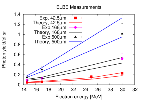
We observe that the lower value of the simulated yield is within 15% of the experimental yield in most cases. This compares to nearly a factor of two difference in the earlier simulations [9]. It is clear that the simulation model with the lower value of can be used to predict the expected yield over this range of thicknesses. We will use the population equations, Eqs. (22), (23), with the lower to calculate the expected yield with ASTA parameters.
4 ASTA simulations
In this section we apply the model to the ASTA photoinjector and calculate the expected X-ray properties including the brilliance. The main parameters of ASTA are shown in Table 7. The major improvement over the ELBE facility is in the transverse emittance of the electron beam. Recent developments have shown that normalized emittances of less than 100 nm can be obtained with a conventional laser photocathode by suitably reducing the laser spot size [24]. Recent studies of field emission based cathodes using needle like structures with tips of 5 nm radius of curvature have shown promising results [25]. Estimates show that the normalized emittances of the electron beam at the needle cathode can be as small as 1 nm. Simulations have shown that this emittance is mostly preserved from the source to the crystal about 5m downstream. Here however we will assume a normalized emittance of 100 nm. Reductions in this emittance will increase the spectral brilliance. Diamond crystals cut parallel to the (110) plane are already available and these will be used for all the studies reported here.
| Beam energy [MeV] | 20 | 50 |
| Bunch charge [pC] | 20 | 20 |
| Bunch frequency [MHz] | 3 | 3 |
| Average beam current [nA] | 300 | 300 |
| Transverse normalized emittance [nm] | ||
| Bunch length [mm] | ||
| Relative energy spread [%] | ||
| Critical angle [mrad] | 1.54 | 0.98 |
4.1 Potential and Populations
Figure 6 shows the real potential with the bound states at 20 MeV and 50 MeV and the imaginary potential. These potentials depend on the crystal lattice and the chosen planes while the number of bound states (shown as bands in the two figures) increase with beam energy roughly as . The depth of the real potential for the (110) plane in diamond is about 23.8 eV while the height of the imaginary potential is about 0.045 eV.


Figure 7 shows the transition probabilities calculated using Eqs. (11) and (LABEL:eq:_Vimag) for the four bound states at 20 MeV. As mentioned earlier, they obey the approximate selection rule if . The diagonal matrix element is the largest for each and decreases with increasing energy transfer as increases. Several conclusions can be drawn from these transition rates. For example, most of the transitions from the lower bound states are to other bound states. At , only 16% of the transitions take an electron to a free state , this increases to 36% from the next bound state and to 52% from . Since the transition rates are larger at lower , the bound states will depopulate faster than the free states will be populated.


Figure 8 shows the probability density of the first three bound states at beam energies of 20 MeV and 50 MeV. The eigenstates have definite parity, consequently the even states have a local maximum at the nucleus while the odd states have a node at the nucleus. We also observe that the probability densities of these states increase slightly with energy and they are more localized around the nucleus at 50 MeV.
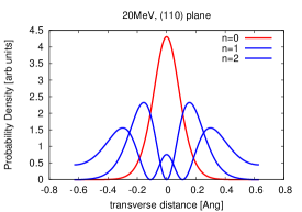
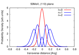
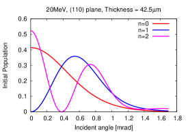
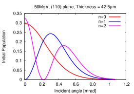
Figure 10 shows the initial population at the entrance of the crystal for different incidence angles. The transverse energy increases with incidence angle and the initial populations in these states also change, in particular being non-zero for the odd states as well. Increased initial population in the state would increase the photon flux in the 10 transitions. At 20 MeV, is maximum at an incidence angle of 0.54 mrad while at 50 MeV, the maximum is at 0.3 mrad.
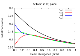
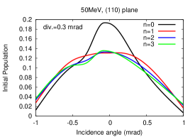
The left plot in Fig.10 shows the initial population as a function of the beam divergence at beam energy of 50 MeV. These populations will be dominated by the electrons incident at close to zero angle. Thus in the even states we observe a slow decrease with divergence and not the oscillations seen in the higher even states in Fig. 10. In the odd states however, the non-zero contributions are due to electrons with non-zero incident angle and thus in the state we observe a slow rise and a broad maximum at a beam divergence of 0.3 mrad, matching the maximum location seen in Fig. 10. This optimum divergence is well below the critical angle 0.98 mrad for channeling at 50 MeV. The right plot in Fig. 10 shows the initial populations as a function of the incidence angle when the beam divergence is set to 0.3 mrad to maximize the population in the state. Now we observe that the maximum in all states is obtained at zero incidence angle, so there is no advantage in tilting the crystal with respect to the beam direction when the beam divergence is optimum. The same observations hold at 20 MeV where the optimum beam divergence is about 0.5 mrad.
From the decay of the populations with distance into the crystal, we find that the occupation lengths are about 9 m with a 42.5 m thick crystal and about 20 m with a 168 m thick crystal. These values are about the same at 20 and 50 MeV and for the different bound states.
4.2 X-ray energies, linewidths, photon yields
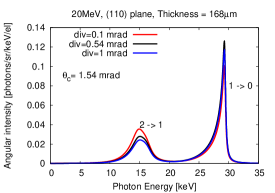
We discuss the X-ray intensity spectrum expected at ASTA and consider the effects of beam divergence on the spectrum. Fig. 11 shows the angular intensity spectrum (photons/sr-electron) with different beam divergences for a crystal thickness of 168 m at two energies. At the beam energy of 20 MeV, the 10 transition leads to the highest peak at 29.3 keV with a width of 1.8 keV while the 21 transition leads to a lower peak at 16.5 keV with a broader width of about 2.1 keV. From our discussion of the ELBE simulations, we expect these linewidths to under-estimate the experimental width by roughly a factor of two.
At a beam energy of 50 MeV there are more bound states and we observe more lines in the spectrum. The highest energy peak is still from the 1 transition at 141.9 keV with a width of 9 keV while the most intense peak is from the 21 transition at 89.3 keV with a width of 5.7 keV. There are also lower energy and less intense lines from the 32 transition at 66.3 keV and from the 43 transition at 53.6 keV.
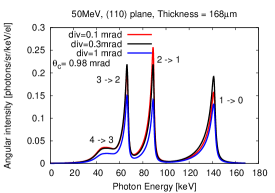
In these calculations, the effect of the beam divergence on the initial populations in the different states is included but not the change of channeling fraction with the divergence. The spectrum with a beam divergence of 0.1 mrad is very close to that of the single electron spectrum for both energies.
At 20 MeV, the yield in the 10 transition at 0.54 mrad divergence is higher compared to the yield at 0.1 mrad, but decreases on further increasing the divergence to 1 mrad. At 50 MeV, similar behavior is observed with the maximum in the 10 and the 32 transitions at a divergence of 0.3 mrad. Since the divergence affects the dechanneling fraction, the observed spectrum may have a somewhat different dependence on the beam divergence.
| Energy | Thickness | Energy | Linewidth | Yield [phot/e-/sr] | |
|---|---|---|---|---|---|
| [MeV] | m | [keV] | [keV] | No dechan. yield | yield |
| 20.0 | 42.5 | 29.3 | 1.21 | 0.27 | 0.075 |
| 168 | 29.3 | 1.85 | 0.77 | 0.17 | |
| 50.0 | 42.5 | 89.3 | 3.83 | 2.7 | 1.00 |
| 42.5 | 141.9 | 6.1 | 2.1 | 0.65 | |
| 168 | 89.3 | 5.65 | 6.6 | 1.7 | |
| 168 | 141.9 | 8.96 | 6.1 | 1.6 | |
Table 8 shows the X-ray energies, linewidths and photon yields expected at ASTA. Based on the ELBE simulations, the energies are expected to be accurate to better than 10%. However the linewidths will be about a factor of two larger than the values in this table, as follows from the discussion in Section 3.2. This table also shows the photon yields for two cases: without enhanced dechanneling and with this dechanneling with the parameter set to the value which under-estimates the yield; see the discussion following Table 6 and Fig. 5.
4.3 Spectral brilliance
A radiation source is usually characterized by the number of photons emitted per second per bandwidth per unit solid angle and unit area of the source, also called the spectral brilliance. The photon yields found above can be used to estimate the expected X-ray spectral brilliance at ASTA. The yield as calculated in Section 4.2 depends on the beam divergence through the dependence of the initial population on the divergence, as shown in Fig. 10. It does not include the likelihood that particles in the distribution with incidence angles greater than the Lindhard critical angle will not be channeled. With the assumption of no rechanneling, the yield could be multiplied by the fraction of particles with incident angles less than ,
| (36) |
where Erf is the error function, is the electron beam divergence and for planar channeling with the depth of the potential.
The average brilliance of the radiation emitted by a beam of electrons can be written in terms of the differential intensity spectrum per electron as
| (37) |
where is the average electron beam current, is the energy of the X-ray line and is the X-ray beam spot size. Expressed in terms of the yield per electron and in a 0.1% band-width we have the average brilliance expressed in typical light source units
| (38) | |||||
is the total photon yield per electron, is the relative width of the X-ray line, and is the normalized emittance in mm-mrad. We set the X-ray beam spot size to the lower limit value of the electron beam spot size , while the X-ray divergence is .

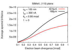
The left plot in Fig. 12 shows the brilliance as a function of X-ray energy at a beam energy of 50 MeV with a beam divergence of 0.1 mrad while the right plot in this figure shows the expected brilliance in the 10 line as a function of the beam divergence for two crystal thicknesses. With the assumptions made above, we observe that that the brilliance is larger with the thicker crystal, the difference increases with divergence and reaches about 70% when the beam divergence equals the Lindhard critical angle.
Table 9 shows the brilliance and photon flux at two energies for a crystal thickness of 168 m, again with the same assumptions as in Figure 12. Since the values quoted are for the beam divergence of 0.1 mrad, the value quoted for the ELBE experiment and used in setting the value of in Eqs. (22) and (23), the deviations from the values to be observed at ASTA may be small.
| Beam energy [MeV] | 20 | 50 |
| Av. beam current [nA] | 300 | 300 |
| Beam emittance [nm] | 100 | 100 |
| Beam divergence [mrad] | 0.1 | 0.1 |
| X-ray energy from [keV] | 29.2 | 141.9 |
| Est. energy spread [keV] | ||
| Angular yield [photons/(e-sr)] | 0.17 | 1.69 |
| Absolute yield/electron [] | 0.11 | 0.17 |
| Av. X-ray brilliance [] | 0.79 | 48.0 |
| Av. Photon flux at [photons/s] | 2.1 | 3.3 |
As steps towards increasing the brilliance, one could consider increasing the beam current either with a higher bunch charge or a higher micropulse repetition rate if the crystal does not suffer damage from heating at the higher currents. A more promising path would be to lower the emittance since the brilliance depends inversely on the square of the emittance. The results above have assumed an electron emittance of 100 nm using a laser photocathode. First tests of operation with a field emission cathode mentioned above have recently been reported [26]. Assuming that success is achieved with these cathodes and that the low emittance generated can be preserved until the crystal, the brilliance could then be increased by about two orders of magnitude above the values reported here.
5 Conclusions
In this report we have studied the expected spectral brilliance of X-rays from channeling experiments to be performed at the ASTA photoinjector. We revisited the theoretical model, corrected the potential describing thermal scattering and developed a heuristic model to include dechanneling in the population dynamics. We used the updated model to first compare with the experimental values reported from the ELBE facility and second to predict values for ASTA.
We compared the energies, linewidths and photon yields from the model with the results at the ELBE facility. With appropriate choices of dechanneling states in the model, the simulated yield agrees well with observed photon yields, see Fig.5. The theoretical linewidth is about a factor of two smaller than the observed values. This is due to the neglect of electron scattering with the atomic electrons and the plasmonic modes. This scattering affects only the linewidth but does not affect the photon yields. From the population dynamics we were able to estimate, for different quantum states, the occupation length whose classical analog is the dechanneling length. The occupation length was found to increase with crystal thickness but was nearly independent of beam energy in the energy range studied. This pointed to the importance of rechanneling in the quantum regime where particles in the free states can be scattered back into the channeled bound states. Rechanneling increases with crystal thickness and explains why the measured occupation lengths are longer than simple classical estimates. We found that the optimum crystal thickness to maximize the intensity of the 10 transition is about 7 times the occupation length.
When applied to ASTA, the model finds that with an electron beam energy of 50 MeV, X-ray peaks are expected at about 142 keV from the 10 transition and at 89 keV from the 21 transition with linewidths around 14%. The ability of channeling radiation to produce hard X-rays with moderate beam energies is one of the main premises for these experiments. We find that with a crystal thickness of 168 m and electron transverse emittances of 100 nm and beam current of 300 nA, the expected brilliance is of the order of 1010 photons/(s-(mm-mrad)2-0.1% BW). It is possible that thicker crystals may increase the brilliance above these values. Significant increase in the brilliance by about two orders of magnitude could be achieved with ultra-low emittance beams using field emitter cathodes and beam studies with these novel cathodes are in progress.
Acknowledgments
We thank the Lee Teng undergraduate internship program at Fermilab which awarded
C. Lynn a summer internship in 2013 when this project began. We thank B. Blomberg,
D. Mihalcea and P. Piot for useful discussions.
Fermilab is operated by Fermi Research Alliance, LLC under Contract
No. DE-AC02-07CH11359 with the United States Department of Energy.
References
- [1] J.U. Andersen, E. Bonderup & R.H. Pantell, Ann. Rev. Nuc. Sci, 33, 453 (1983)
- [2] A.W. Saenz and H. Uberall, Coherent Radiation Sources, Springer, Berlin (1985)
- [3] U. Uggerhoj, Rev. Mod. Phys.,77, 1131 (2005)
- [4] R. Carrigan et al, Phys. Rev. A,68, 062901 (2003)
- [5] P. Piot et al, Fermilab-Conf-13-086-AD-APC, arxiv:1304.0311
- [6] C. Brau et al, Synch. Rad. News, 25, 20 (2012)
- [7] P. Piot et al, AIP Conf. Proc., 1507, 734 (2012)
- [8] W. Wagner et al, Nucl. Instr. & Meth. B, 266, 327 (2008)
- [9] B. Azadegan, Ph.D thesis, Technischen Universitat Munchen (2007)
- [10] R.A. Doyle and P.S. Turner, Acta Crystallogr. A , 24, 390 (1968)
- [11] K. Chouffani & H. Uberall, Phys. Stat. Solidi. B, 213, 107 (1999)
- [12] B. Azadegan et al, Phys. Rev B.,74, 045209 (2006)
- [13] J.U. Andersen et al, Phys. Scr., 28, 308 (1983)
- [14] J.O. Kephart et al, Phys. Rev. B, 40, 4249 (1989)
- [15] H. Genz et al, Phys Rev. B, 53, 8922 (1996)
- [16] C.R. Hall and P.B. Hirsch, Proc. Roy. Soc. A, 286, 158 (1965)
- [17] H. Backe et al, Nucl. Instr. & Meth. B, 266, 3835 (2008)
- [18] R. Carrigan, Int. J. Mod. Phys.A, 55, 55 (2008)
- [19] J. Beringer et al (Particle Data Group), Phys. Rev. D,86, 010001 (2012)
- [20] V.N. Baier, V.M. Katkov and V.M. Strakhovenko, Electromagnetic Processes at High Energies in Oriented Single Crystals, World Scientific (1998)
- [21] U. Nething et al.,Phys. Rev. Lett.,72,2411 (1994)
- [22] http://www.nist.gov/pml/data/xraycoef/index.cfm
- [23] B. Azadegan, Comp. Phys. Comm., 184, 1064 (2013)
- [24] R.K. Li et al, Phys. Rev. ST-AB, 15, 090702 (2012)
- [25] W.E. Gabella et al, Nucl. Instr. & Meth. B, 309, 10 (2013)
- [26] P. Piot et al, Appl. Phys. Lett., 104, 263504 (2014)