Calculation of Energy Band Diagram of a Photoelectrochemical Water Splitting Cell
Abstract
A physical model is presented for a semiconductor electrode of a photoelectrochemical (PEC) cell, accounting for the potential drop in the Helmholtz layer. Hence both band edge pinning and unpinning are naturally included in our description. The model is based on the continuity equations for charge carriers and direct charge transfer from the energy bands to the electrolyte. A quantitative calculation of the position of the energy bands and the variation of the quasi-Fermi levels in the semiconductor with respect to the water reduction and oxidation potentials is presented. Calculated current-voltage curves are compared with established analytical models and measurement. Our model calculations are suitable to enhance understanding and improve properties of semiconductors for photoelectrochemical water splitting.
Zurich University of Applied Sciences] Institute of Computational Physics, Zurich University of Applied Sciences (ZHAW), Wildbachstrasse 21, 8401 Winterthur, Switzerland Ecole Polytechnique Fédérale de Lausanne] Laboratory of Photonics and Interfaces, Ecole Polytechnique Fédérale de Lausanne, EPFL-SB-ISIC-LPI, Station 6, 1015 Lausanne, Switzerland University Jaume I] Photovoltaics and Optoelectronic Devices Group, Departament of Physics, University Jaume I, 12071 Castellon, Spain University Jaume I] Photovoltaics and Optoelectronic Devices Group, Departament of Physics, University Jaume I, 12071 Castellon, Spain Zurich University of Applied Sciences] Institute of Computational Physics, Zurich University of Applied Sciences (ZHAW), Wildbachstrasse 21, 8401 Winterthur, Switzerland Ecole Polytechnique Fédérale de Lausanne] Laboratory of Photonics and Interfaces, Ecole Polytechnique Fédérale de Lausanne, EPFL-SB-ISIC-LPI, Station 6, 1015 Lausanne, Switzerland Zurich University of Applied Sciences] Institute of Computational Physics, Zurich University of Applied Sciences (ZHAW), Wildbachstrasse 21, 8401 Winterthur, Switzerland
Introduction
Research on hydrogen production by photoelectrochemical (PEC) cells is propelled by the worldwide quest for capturing, storing and using solar energy instead of decreasing fossil energy reserves. Hydrogen is widely considered as a key solar fuel of the future 1. Hydrogen is also part of power to gas conversion systems developed to resolve intermittency in the wind and solar energy production 2. Although a PEC/photovoltaic cell with 12.4% efficiency was demonstrated with GaInP2/GaAs 3, decreasing its cost and increasing its lifetime are still under way. An alternative approach often pursued is to use abundant and cheap metal oxides as a viable class of semiconductor materials for PEC electrodes 4, 5, 6. However, their recombination losses, charge carrier conduction and water oxidation properties need to be understood and optimized both by measurement and numerical simulation 7.
Several approaches for a mathematical analysis of semiconductor electrodes can be found in the literature, including analytical 8, 9 and numerical models 10, 11 of PEC cells. An extensive numerical study of PEC behavior of Si and GaP nanowires was recently conducted with commercial software 12. Since surface states play a major role for many semiconductors, corresponding models were also developed to analyze their effect on electrochemical measurements 13, 14, 15. On the PEC system level, models of the coupled charge and species conservation, fluid flow and electrochemical reactions were recently developed 16, 17. The latter studies revealed how PEC systems should be designed with minimal resistive losses and low crossover of hydrogen and oxygen by use of a non-permeable separator.
Almost every publication on PEC cells features a schematic energy band diagram of a PEC cell, mostly sketched by hand from basic physical understanding described in textbooks on electrochemistry 18, 19, 7. Although such sketches might be qualitatively correct, numerical calculations of the charge carrier transport might reveal additional features not captured by the sketches. We are aware that the development of numerical calculations is frequently hindered by the complicated physical processes in the actual materials and lack of measurements of parameter values for these processes 20. In spite of these obstacles, we think that the recent advent of user-friendly numerical software and advanced measurement techniques could fill the gap between experimental and numerical approaches if experimentally validated models are developed.
Model
In this work, we present calculation of an energy band diagram of a PEC electrode from a physical model with clearly formulated assumptions 21. The model is based on charge carrier continuity equations with direct charge transfer from the valence or conduction band to the electrolyte. We consider a PEC cell consisting of an n-type semiconductor with bandgap energy , and an electrolyte which can easily accept a single electron or hole (such as H2O2 22 or [Fe(CN)6]3-/4- 23). Charge transfer occurs across the semiconductor/electrolyte interface until an equilibrium charge distribution is reached and the equilibrium Fermi level in the semiconductor becomes equal to the redox Fermi level
| (1) |
We reserve subscript for equilibrium values in the dark in the following. To derive our model, we use and repeat some of the general definitions introduced in our previous work 24 shown in 1. Note that we use notation of subscript for semiconductor, for surface quantity, for a bulk semiconductor quantity (where electrons and hole remain at equilibrium in the dark).
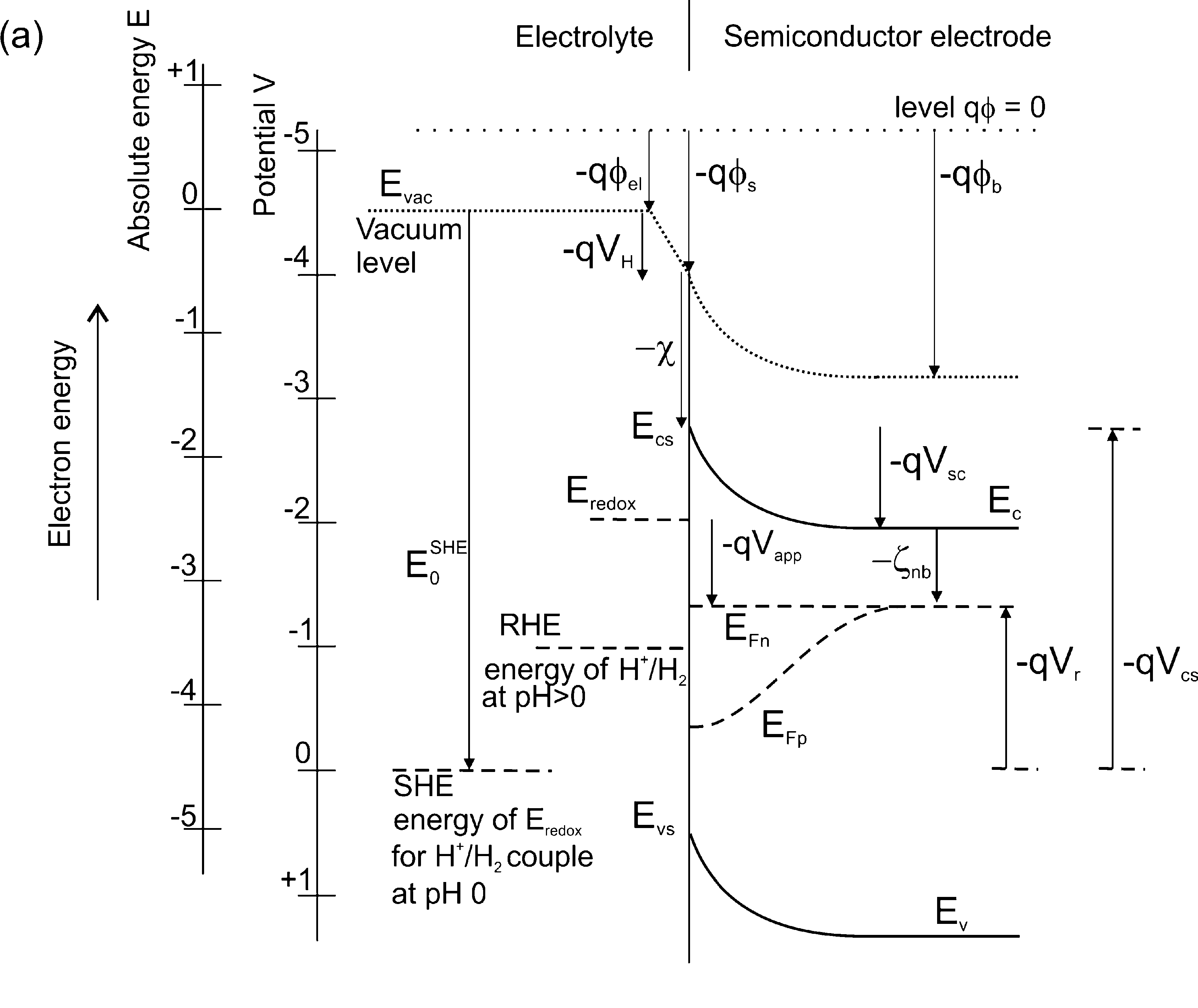
Bulk equilibrium properties of the isolated semiconductor are denoted with a subscript . The bulk of the semiconductor is electrically neutral, hence the concentration of electrons in the bulk must be equal to the number of fully ionized donors , . Thus, the concentration of holes is , where denotes intrinsic carrier concentration. An isolated unbiased semiconductor before contact to an electrolyte has a conduction band edge and a Fermi level related to the vacuum level and electron affinity by
| (2) | |||||
| (3) | |||||
| (4) |
where is the Boltzmann constant, is the temperature, is the elementary charge and the effective density of states in the conduction band, and is the distance of the conduction band edge to Fermi level. In the following, we use =0 eV as usual. The potential drop in the Helmholtz layer in the dark is calculated from the local vacuum level (LVL) at the surface of the semiconductor () and LVL of the electrolyte (), 1,
| (5) |
Note that the potential drop in the Helmholtz layer can be a different value at flatband situation (denoted ) than at other measurable voltage (denoted . We measure the voltage of the semiconductor electrode with respect to a reference electrode, which means the difference of the Fermi level of electrons in the semiconductor back contact and Fermi level of the reference electrode
| (6) |
In this article, we use both the Standard Hydrogen Electrode (SHE) energy and Reversible Hydrogen Electrode (RHE) as reference electrodes and scale of energy. Measured voltage with respect to the SHE is denoted (without subscript SHE) and measurable voltage with respect to the RHE with
| (7) |
where is thermal voltage and denotes pH value of the solution. We draw attention to the fact that negative bias versus RHE brings the energy closer to the vacuum level . The position of the electron Fermi level at the semiconductor back contact is calculated as (see 1)
| (8) |
where denotes the potential drop in the semiconductor. What is usually reported in the literature is the value of flatband potential, which is the measurable voltage when the bands are flat ()
| (9) |
The value of is often not known as it depends on the surface conditions of the semiconductor in the electrolyte. For this article, we know values of and and determine from the last equation. The potential drop in the semiconductor can be expressed from 1 as
| (10) |
Then from eqs. 6, 8, 9 follows
| (11) |
The second option is to refer the voltage to the equilibrium of semiconductor-electrolyte interface (SEI) and this value is denoted 24
| (12) | |||||
| (13) |
where built-in voltage is denoted and potential drop across the Helmholtz layer in dark equilibrium . Equilibrium of SEI means V.
On the semiconductor side of the junction, the electrostatic potential is obtained by solving Poisson’s equation 19
| (14) |
where is the permittivity of vacuum, is the relative permittivity of the semiconductor, is the concentration of fully ionized donors, is the concentration of free electrons and is the concentration of free holes ( for n-type semiconductor in the dark). We can write for the conduction and the valence band edge energies and in the electrostatic potential
| (15) | |||||
The band edge pinning (constant value of and ) is present if for any measurable voltage (assumed in the following), otherwise the band edges become unpinned.
A simple approximation to solve Poisson’s equation, Eq. 14, is to assume that the total space charge is uniformly distributed inside the space charge region (SCR) of width (also called depletion region approximation)
| (16) |
The boundary conditions for the electrostatic potential follow directly from the definitions on 1
| (17) | |||||
| (18) |
The concentration of free electrons and holes in the dark and can be written as
| (19) | |||||
| (20) |
The value of electrostatic potential in the semiconductor bulk appears in the above expressions because we have made general definition of electrostatic potential including the potential drop in the Helmholtz layer. Therefore, is not zero unlike recent textbook definition 7. The approximate solution of Poisson’s eq. is then
| (21) | |||||
When the measurable voltage is positive of the flatband potential , the n-type semiconductor is in the depletion regime. When the measurable voltage is negative of the flatband potential, the semiconductor is in the accumulation regime (due to the sign of ).
Upon illumination, we assume low-injection conditions with the number of photogenerated electrons lower than the donor concentration. Thus electron concentration is roughly equal to the dark electron concentration . The hole continuity equation is solved to obtain free hole concentration inside of the semiconductor of thickness
| (22) |
We consider the generation rate of charge carriers from the simple Lambert-Beer law , where is number of photons with energy above which are absorbed in the semiconductor, is the spectral photon flux of standard AM15G spectrum with intensity 100 mW/cm2 25, is the absorption coefficient of the semiconductor. The hole current density is expressed using the analytical solution of Poisson’s equation
| (23) |
where is the hole mobility, and is the hole diffusion constant. A direct band-to-band nonlinear recombination is assumed
| (24) |
We assume that charge transfer under illumination occurs exclusively from the valence band to the electrolyte. We do not include charge transfer from surface states in the current analysis. The transfer current density of valence band holes at the SEI is described by a first-order approximation 26
| (25) |
where is the rate constant for hole transfer, and a linear dependence on the deviation of the interfacial hole concentration from its dark value at the interface is assumed. Since the thickness of the semiconductor is in the order of the penetration length of light for the hematite parameters listed in 1, we consider the hole current at the back contact of the semiconductor to depend on a surface recombination velocity
| (26) |
We use m/s for numerical calculations throughout this article 12. In order to obtain convergence of the numerical solution procedure, the continuity equation was solved in a non-dimensional form after applying the usual normalization of the variables of the drift-diffusion equations 27.
The quasi-Fermi energies under the influence of an electrostatic potential are calculated by the Boltzmann distribution
| (27) | |||
| (28) |
Results
We numerically solved the hole (electron) continuity equation Eq. 22 for a n-type (p-type) semiconductor by using the depletion region approximation of the electrostatic potential Eq. 21. Results for n-type Fe2O3 and p-type Cu2O are presented in the following. If not otherwise stated, we assume V and in the following.
Fe2O3
The charge carrier concentration profiles calculated from the model are plotted in 2. In the dark, the SCR is depleted of electrons and the concentrations of holes is increased with respect to the bulk hole concentration. For increasing , the dark electron concentration at the SEI decreases until it is smaller than the dark hole concentration at the SEI , leading to an inversion layer characterized by a larger concentration of holes (minorities) than electrons (majorities) in the SCR. Corresponding value of V and thus V are obtained. Therefore, a more detailed future model should take into account the electron continuity equation instead of assuming that the electron concentration upon illumination is equal to the electron concentration in the dark.
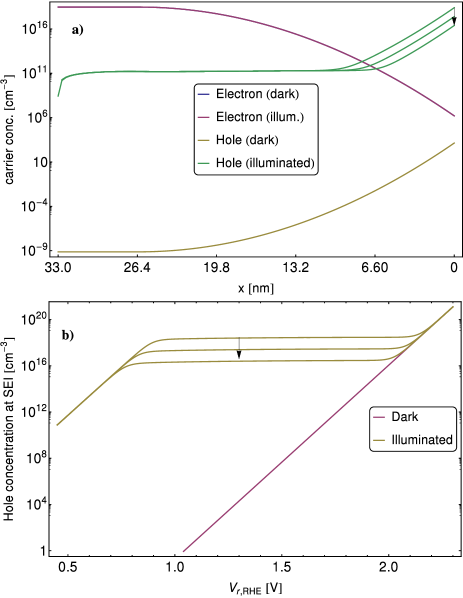
Upon illumination, the concentration of electrons is equal to the dark electron concentration. Less holes are accumulated near the SEI for increasing rate constant (faster charge transfer), 2. For large (¿2.0 V), the hole concentration upon illumination near the SEI approaches the hole concentration in the dark, 2b. At the back contact, the hole concentration follows from solution of continuity equation and boundary condition eq. 26.
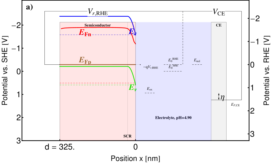
The energy band diagram is shown for a three-electrode setup in 3. A measurable voltage of V is assumed, which is the standard voltage used for comparison of different PEC electrodes 28, 29. The measurable voltage is indicated in 3a) with an arrow on the energy scale, . This is also explained in our previous work 24. The band edges of the semiconductor for flatband condition () are shown as dashed lines, whereas those away from flatband condition () are shown as solid lines. Band positions at flatband conditions for hematite agree well with values reported for example for 30, 31 and 32. An upward band bending of the semiconductor is present if V is more positive than , see 3. Band edges are pinned at the SEI by default (since we assume ), but we allow for modification of surface conditions by changing the value of in our interactive band diagram software 21.
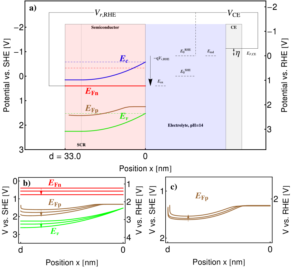
The number of photogenerated electrons is small compared to the donor concentration, and thus illumination does not change the electron concentration. Therefore, the electron quasi-Fermi level is also constant across the semiconductor, eq. 27, and . The position of relative to in the energy diagram is given by arrow , eq. 8. In contrast, the hole concentration is determined mainly by photogenerated holes, which are redistributed in the semiconductor according to the continuity equation Eq. 22. Since is more positive than , a transfer of holes from the valence band can thermodynamically oxidize the electrolyte species. An external wire electrically connects the semiconductor to the metal counter electrode (CE) through a potentiostat. The counter electrode Fermi level is automatically adjusted by applying a voltage above the water reduction energy (including the electrochemical overpotential ) by the potentiostat to enable hydrogen evolution at the counter electrode. The counter electrode is shown in the energy diagram only to completely describe a three-electrode setup and we ignore its polarization in the following 33. In the electrolyte, we plot two reference electrode energies and , standard water reduction and oxidation energy (0 eV vs RHE) and (1.23 eV vs RHE). Note that the relation of and to depends on the concentrations (activities) of oxidizing and reducing species in the solution 34.
The energy band diagram in the semiconductor for different values of the measurable voltage is plotted in 3b). For increasing the band bending increases and the electron quasi-Fermi level shifts down on the RHE scale. Interestingly, the hole quasi-Fermi level at the SEI remains nearly constant for increasing (see Figure S1 in Supporting Information) and thus the splitting of the quasi-Fermi levels (photovoltage) approaches zero. In the neutral region , the hole quasi-Fermi level is more negative for increasing and the photovoltage is nearly constant. When the hole diffusion length is increased, the flat region of the hole quasi-Fermi level near the SEI is enlarged, 3c), and the hole concentration in the neutral region decreases (see Figure S2 in Supporting Information).
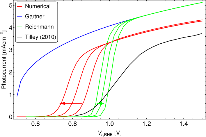
We simulated current-voltage curves with our numerical model (eq. 25) and compared the results with published models of Gartner 8 and Reichmann 10, 4. According to Gartner, the minority charge carrier concentration is calculated from the diffusion equation, neglecting recombination in the SCR and assuming that every hole in SCR contributes to the photocurrent. Photocurrent density of Gartner is
| (29) |
Therefore, overestimates the minority carrier photocurrent in comparison to our numerical model . Recombination in the SCR by Sah-Noyce-Shockley formalism was incorporated into the model by Reichmann 10 with resulting photocurrent (the detailed expression is given in the Supporting Information). For small , is much smaller than because the SCR recombination loss is included in . The onset of the photocurrent calculated by Reichmann starts when ( is the saturation current density as defined in the SI). Therefore, if we consider faster charge transfer kinetics (larger ), we need a smaller value of the onset potential (and thus ) to obtain a similar value . For increasing , approaches because the SCR recombination becomes negligible in 10, but the numerical photocurrent is smaller than since SCR recombination is included in . The numerical photocurrent onsets when is more positive than and it is larger than for small . Increasing the rate constant represents a faster exchange rate of holes with the solution. This also shifts the numerical j-V curve to the left as predicted by the Reichmann model, decreasing the onset potential of the photocurrent.
Measured current-voltage curve for nanostructured Fe2O3 electrode with IrO2 catalyst 35 is compared with the prediction from our model on 4. The onset voltage of measured photocurrent 0.8 VRHE is reproduced with numerical photocurrent with = 10-4 m/s. However, the slope of measured photocurrent and its value 4.3 mA/cm2 at 1.5 Vr,RHE is smaller than the slope of numerical photocurrent and its value 3.8 mA/cm2 at 1.5 Vr,RHE. These differences point out that we cannot verify our model description by comparing the current-voltage curves alone, because the kinetic effects cannot be distinguished in the current-voltage response. Comparison of the model predictions with impedance spectroscopy 36 measurements is needed to verify the model.
We checked that the maximum photocurrent obtainable from the hematite electrode based purely on the number of absorbed photons is mA/cm2 for AM15G illumination. This value is also obtained for the Gartner photocurrent eq. 29 when the bracket term is close to one and also for the Reichmann photocurrent (which recovers the Gartner photocurrent in regime of large voltages). The plateau of numerical photocurrent cannot be computed here, because our model cannot be used to predict photocurrents at voltages higher than . At such voltages inversion layer is formed as described in the previous text and this would need degenerate statistics to be included in the model.
Cu2O
We also applied our model to simulate p-type semiconductors for photocathodes. Appropriate changes in the equations were introduced, resulting from doping with acceptors rather than donors. Cuprous oxide (Cu2O) is an abundant and promising material for PEC photocathodes. The main issue with Cu2O is its limited stability in water, which is currently being addressed with stabilizing overlayers 37, 38, 39. A downward band-bending occurs when is more negative than . This leads to a drift of electrons to the electrolyte, 5. Upon illumination, the hole concentration is assumed to remain equal to the dark hole concentration. The electron concentration is calculated from the electron continuity equation. Electrons are accumulated near the SEI where they reduce water to H2 with a rate constant .
In the case of p-type Cu2O, the majority carriers are holes, and thus the counter electrode carries out the oxidation reaction (including the associated overpotential ). Although the electron quasi-Fermi level is negative with respect to making it suitable for hydrogen evolution, 5, corrosion prevents hydrogen evolution in the experiment unless the Cu2O is protected by overlayers 37. So far, our model does not consider corrosion; here we aimed at showing the general energetic configuration of a p-type PEC photoelectrode.
Conclusion
We presented a physical model for minority charge carrier transport in semiconductor PEC electrodes in contact with an electrolyte. Direct charge transfer to the electrolyte from valence or conduction band, band-to-band recombination and Lambert-Beer optical generation were assumed. A numerical solution of the model equations allows us to calculate the minority carrier concentration and the quasi-Fermi level. A resulting energy band diagram of a PEC cell accounts for the potential drop in the Helmholtz layer and it is capable of modeling both band edge pinning and unpinning. Comparison of the numerically obtained photocurrent with analytical results and measurement reveals need for verification of the model with spectroscopic measurements. Our model was implemented in an interactive software that can be freely accessed online 21. All presented results of this article can be reproduced with this software and we invite all members of the research community to use it while designing PEC cells. We are currently working on an extension of our model to a fully coupled drift-diffusion model with surface states. Such photoelectrode models need to accompany the experimental studies to suppress recombination losses (e.g. by surface passivation) and enhance charge transfer (e.g. by catalysis), the two major issues for efficient metal oxide photoelectrodes 40.
We thank F.T. Abdi, H. J. Lewerenz, G. Schlichthoerl and B. Klahr for fruitful discussions. Financial support by the Swiss Federal Office of Energy (PECHouse2 project, contract number SI/500090-02) is gratefully acknowleged.
| Symbol | Fe2O341 | Cu2O 38, 42 | Description |
| [cm-3] | 0 | Donor concentration | |
| [cm-3] | 0 | Acceptor concentration | |
| [V] | +0.5 | +0.8 | Flatband potential |
| [eV] | +4.7843, 44 | +4.22 43 | Electron affinity |
| [cm-3 | 45, 46 | Density of states of CB | |
| [cm-3] | Density of states of VB | ||
| 32 glasscock_structural_2008 | 6.6 | Relative permitivity | |
| [eV] | 2.1 | 2.17 | Bandgap energy |
| [nm] | 33 | 325 | Thickness of semiconductor |
| [ns] | - | 0.25 | Electron lifetime |
| [ns] | 0.04847 | - | Hole lifetime |
| [nm] | - | 40 | Electron diffusion length |
| [nm] | 5 7 | - | Hole diffusion length |
| [cm-1] | Absorption coefficient | ||
| 14 | 4.9 | pH value of the electrolyte |
| Symbol | Unit | Description |
|---|---|---|
| CE | Counter electrode | |
| LVL | Local vacuum level | |
| PEC | Photoelectrochemical | |
| SCR | Space-charge region | |
| SEI | Semiconductor-electrolyte interface | |
| SHE | Standard hydrogen electrode | |
| SI | Supporting information | |
| RHE | Reversible hydrogen electrode | |
| Subscript i | Quantity in the isolated semiconductor before contact to an electrolyte | |
| Subscript b | Quantity in the semiconductor bulk | |
| Subscript s | Quantity at the SEI | |
| eV/K | Boltzmann constant ( eV/K) | |
| K | Temperature (300 K) | |
| C | Elementary charge ( C) | |
| V | Thermal voltage (25.9 mV) | |
| Js | Planck’s constant ( Js) | |
| m/s | Speed of light in vacuum (299792458 m/s) | |
| V | Measurable voltage with respect to SHE reference electrode | |
| V | Measurable voltage with respect to RHE | |
| V | Measurable voltage with respect to RHE when the inversion layer starts to form | |
| V | Flatband voltage with respect to SHE | |
| V | Flatband voltage with respect to RHE | |
| V | Applied voltage to the semiconductor with respect to the dark equilibrium (unbiased) | |
| V | Potential (voltage) drop across the Helmholtz layer in the dark | |
| V | Potential (voltage) drop across the Helmholtz layer at flatband situation in the dark | |
| V | Potential (voltage) drop across the Helmholtz layer in the dark equilibrium | |
| V | Potential (voltage) drop across the semiconductor | |
| V | Built-in voltage of semiconductor/liquid junction | |
| V | Voltage between the reference electrode and counterelectrode | |
| V | Electrochemical overpotential at the CE | |
| eV | Energy of the local vacuum level | |
| eV | Energy of the SHE with respect to vacuum level of the electron (-4.44 eV) | |
| eV | Energy of the RHE with respect to vacuum level of the electron | |
| eV | Fermi level of the electrolyte species (redox level) | |
| eV | Standard water reduction energy | |
| eV | Standard water oxidation energy | |
| eV | Equilibrium Fermi level in the semiconductor (dark) | |
| eV | Conduction band edge in the isolated semiconductor before contact to an electrolyte | |
| eV | Fermi level in the isolated semiconductor before contact to an electrolyte | |
| , | eV | Quasi-Fermi energy of electrons and holes |
| eV | Quasi-Fermi energy of electrons at the back contact | |
| eV | Conduction band edge in the semiconductor | |
| eV | Valence band edge in the semiconductor | |
| eV | Fermi level of the CE | |
| eV | The difference between the semiconductor conduction band energy and the electron Fermi level | |
| V | Local electrostatic potential | |
| V | Approximate solution for local electrostatic potential | |
| V | Local electrostatic potential of the electrolyte | |
| V | Local electrostatic potential at SEI | |
| V | Local electrostatic potential in the semiconductor bulk |
Table 2 continuted. Symbol Unit Description m-3 Intrinsic carrier concentration in the bulk of semiconductor , m-3 Equilibrium concentration of electrons and holes in the bulk of isolated semiconductor , m-3 Dark concentration of electrons and holes , m-3 Concentration of electrons and holes m Width of the space-charge region in the semiconductor A/m2 Hole current density A/m2 Current density calculated by Gartner 8 A/m2 Current density calculated by Reichmann10 A/m2 Saturation current density , m-3s-1 Generation and recombination rate of holes m-2s-1 Number of photons absorbed in the semiconductor from AM15G spectrum m-3s-1 Spectral photon flux of AM15G spectrum m2V-1s-1 Mobility of holes m2s-1 Diffusion constant of holes ms-1 Rate constant for charge transfer of VB holes to electrolyte m Wavelength below which semiconductor absorbs photons ms-1 Back contact surface recombination velocity
References
- Lewis and Nocera 2006 Lewis, N. S.; Nocera, D. G. Proceedings of the National Academy of Sciences 2006, 103, 15729–15735
- Schiermeier 2013 Schiermeier, Q. Nature 2013, 496, 156–158
- Khaselev and Turner 1998 Khaselev, O.; Turner, J. A. Science 1998, 280, 425–427
- van de Krol and Liang 2013 van de Krol, R.; Liang, Y. CHIMIA International Journal for Chemistry 2013, 67, 168–171
- Sivula 2013 Sivula, K. CHIMIA International Journal for Chemistry 2013, 67, 155–161
- Abdi et al. 2013 Abdi, F. F.; Han, L.; Smets, A. H. M.; Zeman, M.; Dam, B.; van de Krol, R. Nature Communications 2013, 4, year
- Krol and Grätzel 2011 Krol, R. V. D.; Grätzel, M. Photoelectrochemical Hydrogen Production; Springer, 2011
- Gärtner 1959 Gärtner, W. W. Physical Review 1959, 116, 84–87
- Wilson 1977 Wilson, R. H. Journal of Applied Physics 1977, 48, 4292–4297
- Reichman 1980 Reichman, J. Applied Physics Letters 1980, 36, 574–577
- Andrade et al. 2011 Andrade, L.; Lopes, T.; Ribeiro, H. A.; Mendes, A. International Journal of Hydrogen Energy 2011, 36, 175–188
- Foley et al. 2012 Foley, J. M.; Price, M. J.; Feldblyum, J. I.; Maldonado, S. Energy & Environmental Science 2012, 5, 5203–5220
- Peter et al. 1984 Peter, L.; Li, J.; Peat, R. Journal of Electroanalytical Chemistry and Interfacial Electrochemistry 1984, 165, 29–40
- Klahr et al. 2012 Klahr, B.; Gimenez, S.; Fabregat-Santiago, F.; Hamann, T.; Bisquert, J. J. Am. Chem. Soc. 2012, 134, 4294–4302
- Bertoluzzi and Bisquert 2012 Bertoluzzi, L.; Bisquert, J. The Journal of Physical Chemistry Letters 2012, 2517–2522
- Carver et al. 2012 Carver, C.; Ulissi, Z.; Ong, C.; Dennison, S.; Kelsall, G.; Hellgardt, K. International Journal of Hydrogen Energy 2012, 37, 2911–2923
- Haussener et al. 2013 Haussener, S.; Hu, S.; Xiang, C.; Weber, A. Z.; Lewis, N. Energy & Environmental Science 2013
- Salvador 2001 Salvador, P. The Journal of Physical Chemistry B 2001, 105, 6128–6141
- Memming 2008 Memming, R. Semiconductor Electrochemistry; John Wiley & Sons, 2008
- Peter 2013 Peter, L. M. Journal of Solid State Electrochemistry 2013, 17, 315–326
- 21 Cendula, P. The model is available freely on the internet. http://icp.zhaw.ch/PEC
- Dotan et al. 2011 Dotan, H.; Sivula, K.; Grätzel, M.; Rothschild, A.; Warren, S. C. Energy & Environmental Science 2011, 4, 958
- Klahr and Hamann 2011 Klahr, B. M.; Hamann, T. W. Applied Physics Letters 2011, 99, 063508–063508–3
- Bisquert et al. 2013 Bisquert, J.; Cendula, P.; Bertoluzzi, L.; Gimenez, S. The Journal of Physical Chemistry Letters 2013, 205–207
- NREL 2012 NREL, Solar Spectral Irradiance: Air Mass 1.5, downloaded March 2012, 2012. http://rredc.nrel.gov/solar/spectra/am1.5/
- Tan et al. 1994 Tan, M. X.; Laibinis, P. E.; Nguyen, S. T.; Kesselman, J. M.; Stanton, C. E.; Lewis, N. S. Principles and Applications of Semiconductor Photoelectrochemistry. In Progress in Inorganic Chemistry; Karlin, K. D., Ed.; John Wiley & Sons, Inc., 1994; pp 21–144
- Markowich et al. 1990 Markowich, P. A.; Ringhofer, C. A.; Schmeiser, C. Semiconductor equations; Springer-Verlag New York, Inc.: New York, NY, USA, 1990
- Kay et al. 2006 Kay, A.; Cesar, I.; Grätzel, M. J. Am. Chem. Soc. 2006, 128, 15714–15721
- Chen et al. 2013 Chen, Z.; Deutsch, T. G.; Dinh, H. N.; Domen, K.; Emery, K.; Forman, A. J.; Gaillard, N.; Garland, R.; Heske, C.; Jaramillo, T. F.; Kleiman-Shwarsctein, A.; Miller, E.; Takanabe, K.; Turner, J. Efficiency Definitions in the Field of PEC. In Photoelectrochemical Water Splitting; SpringerBriefs in Energy; Springer New York, 2013; pp 7–16
- Nozik 1978 Nozik, A. J. Annual Review of Physical Chemistry 1978, 29, 189–222
- Grätzel 2001 Grätzel, M. Nature 2001, 414, 338–344
- Krol et al. 2008 Krol, R. v. d.; Liang, Y.; Schoonman, J. J. Mater. Chem. 2008, 18, 2311–2320
- Hodes 2012 Hodes, G. The Journal of Physical Chemistry Letters 2012, 3, 1208–1213
- Morrison 1980 Morrison, S. R. Electrochemistry at semiconductor and oxidized metal electrodes; Plenum Press, 1980
- Tilley et al. 2010 Tilley, S. D.; Cornuz, M.; Sivula, K.; Grätzel, M. Angewandte Chemie 2010, 122, 6549–6552
- Klahr et al. 2012 Klahr, B.; Gimenez, S.; Fabregat-Santiago, F.; Bisquert, J.; Hamann, T. W. Energy & Environmental Science 2012, 5, 7626–7636
- Paracchino et al. 2011 Paracchino, A.; Laporte, V.; Sivula, K.; Grätzel, M.; Thimsen, E. Nat Mater 2011, 10, 456–461
- Paracchino et al. 2012 Paracchino, A.; Mathews, N.; Hisatomi, T.; Stefik, M.; Tilley, S. D.; Grätzel, M. Energy & Environmental Science 2012, 5, 8673
- Tilley et al. 2013 Tilley, S. D.; Schreier, M.; Azevedo, J.; Stefik, M.; Graetzel, M. Advanced Functional Materials 2013, n/a–n/a
- Sivula 2013 Sivula, K. The Journal of Physical Chemistry Letters 2013, 4, 1624–1633
- Upul Wijayantha et al. 2011 Upul Wijayantha, K.; Saremi-Yarahmadi, S.; Peter, L. M. Physical Chemistry Chemical Physics 2011, 13, 5264
- Paracchino et al. 2012 Paracchino, A.; Brauer, J. C.; Moser, J.-E.; Thimsen, E.; Graetzel, M. The Journal of Physical Chemistry C 2012, 116, 7341–7350
- Xu and Schoonen 2000 Xu, Y.; Schoonen, M. A. A. American Mineralogist 2000, 85, 543–556
- Niu et al. 2010 Niu, M.; Huang, F.; Cui, L.; Huang, P.; Yu, Y.; Wang, Y. ACS Nano 2010, 4, 681–688
- Morin 1954 Morin, F. J. Physical Review 1954, 93, 1195–1199
- Cesar et al. 2008 Cesar, I.; Sivula, K.; Kay, A.; Zboril, R.; Grätzel, M. J. Phys. Chem. C 2008, 113, 772–782
- Bosman and van Daal 1970 Bosman, A.; van Daal, H. Advances in Physics 1970, 19, 1–117