PtSi Clustering In Silicon Probed by Transport Spectroscopy
Abstract
Metal silicides formed by means of thermal annealing processes are employed as contact materials in microelectronics. Control of the structure of silicide/silicon interfaces becomes a critical issue when the device characteristic size is reduced below a few tens of nanometers. Here we report on silicide clustering occurring within the channel of PtSi/Si/PtSi Schottky barrier transistors. This phenomenon is investigated through atomistic simulations and low-temperature resonant tunneling spectroscopy. Our results provide evidence for the segregation of a PtSi cluster with a diameter of a few nanometers from the silicide contact. The cluster acts as metallic quantum dot giving rise to distinct signatures of quantum transport through its discrete energy states.
In the recent years extensive research has been devoted to the replacement of the heavily-doped silicon contact regions of conventional metal-oxide-semiconductor fied-effect-transistors (MOSFETs) with metallic binary compounds of silicon and a transition element, generally referred to as metal silicides Larson and Snyder (2006). This approach aims at reducing source/drain contact resistances and, simultaneously, relaxing the constrains imposed by doping-profile control. In addition, a lower thermal budget can be expected from the use of relatively low-temperature silicidation processes, as opposed to the high-temperature annealing cycles required for dopant activation. The removal of heavily doped contact regions is not priceless though. In fact, an undesirable Schottky barrier (SB) is introduced with a negative impact on device performances. The SB reduces the on-state current and decreases the sub-threshold slope, leading to a poorer switching performance of the MOSFET. This problem can be mitigated by choosing silicides with low SB height. The high working function of platinum silicide (PtSi) makes this compound the best candidate for contacts to p-type silicon channels. The reported values for the SB height, , in PtSi/p-Si junctions range between and eV Dubois and Larrieu (2004). The attractiveness of PtSi is not only limited to p-channel SB transistors. This metal silicide has been successfully used also for the fabrication of inverters in complementary MOS technology where it forms the contact material of both p-type and n-type transistors Larrieu and Dubois (2011). In the latter case, the formation of the silicide is accompanied by the accumulation of n-type dopants (typically As or P) close to the PtSi/n-Si interface leading to a suppression of the effective SB height. This approach avoids the integration of a second silicide for n-type contacts, typically ErSiJang et al. (2005) or YSiZhu et al. (2004). Furthermore, PtSi is routinely used in p-type Schottky diodes for infrared photo detection Shigeyuki (1992); Lin et al. (1995).
PtSi, and metal silicides in general, are formed through a thermally activated process. Upon annealing of a thin Pt film on Si, the two materials diffuse into each other Poate and Tisone (1974). (This differs from the case of other commonly used silicides, e.g. nickel silicide, where essentially only the metal element acts as a diffusing species.) Contact fabrication relies on an accurate control of this inter-diffusion process, which leads to the formation of a silicide phase. In particular, the achievement of sharp boundary between PtSi and Si is important in order to meet the demand for device scaling down to characteristic channel lengths of only a few tens of nm. Non-abrupt interfaces, and the possible simultaneous diffusion of metal impurities into the channel region, can alter important figures of merit such as the sub-threshold slope of the on-state current leading to an unacceptably high device variability Asenov et al. (2003). Although thermal annealing can result in atomically abrupt silicide/silicon interfaces Lin et al. (2008), often this is not the case and various degrees of interface roughness can be foundDellas et al. (2012-09-01); Laszcz et al. (2006); Liu et al. (2007). In addition, several experimental evidences of unintentional Pt impurities in the channel of silicon MOSFETs have been reported Calvet et al. (2008a, 2011, b). Such Pt atoms originate during the silicidation process as a result of a diffusive motion from the PtSi/Silicon interface into the Si channel. Yet little is known about their most favorable arrangement within the silicon crystal and, in particular, about how this arrangement is affected by collective interactions among multiple Pt impurities. In this Letter we address this problem through a combined theoretical and experimental study involving atomistic simulations and transport measurements in short-channel PtSi/Si/PtSi SB transistors.
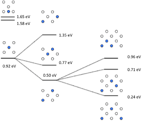
We begin from the simplest case of a single Pt impurity in a Si lattice. Some experimental studies suggest that isolated Pt impurities can indeed be found in the Si region adjacent to a PtSi/Si interface Mantovani et al. (1986); Prabhakar et al. (1983). It has already been shown experimentally and theoretically that in such a case the substitutional position (i.e. a Pt impurity at the place of a Si atom) is the most energetically favorable configuration Watkins and Williams (1995); Anderson et al. (1991, 1992); Woodbury and Ludwig (1962). Here we consider the problem of multiple Pt impurities in a Si lattice. We intend to evaluate the possibility that nearby impurities out-diffusing from a PtSi contact can aggregate into small clusters. We also intend to find the most stable cluster structure.
In order to tackle the problem of multiple Pt impurities we used numerical calculations based on density-functional theory dft . Starting from a single substitutional Pt, we identified the most energetically favorable position for a second substitutional Pt. This identification was accomplished by comparing three different options: first, second, and third neighboring lattice site. As a next step, starting from the most stable two-atom configuration, we studied three possible scenarios for the addition of a third Pt atom. Notice that, given the large difference between the formation energies of interstitial and substitutional single Pt, we ruled out aggregates involving interstitial Pt.
A branched diagram summarizing the results of these total-energy calculations is shown in Fig. 1. Two observations can be made: (i) a driving force promoting aggregation exists each time the formation energy per atom decreases following the addition of Pt atom; (ii) given a set of possible configurations promoting aggregation, substitution as a second neighbor of the pre-existing Pt atom(s) is always preferred. Hence, both first- and second-neighbor substitution are favored for the two-impurity aggregate, as the formation energy per atom decreases from 0.92 eV to 0.77 and 0.5 eV, respectively, the latter being the most stable. When a third Pt atom reaches the second-neighbour two-atom aggregate, on the other hand, the only configuration that leads to an increased stability is the one where all the Pt atom are second neighbors. The other cases considered feature an increase of the formation energy per impurity (0.71 and 0.96 eV) 111For the sake of simplicity we are assuming that, in the slow-rate limit, Pt atoms reaches the clustering zone one by one. We believe, however, that this simplified model is enough to capture the physics of the aggregation process..
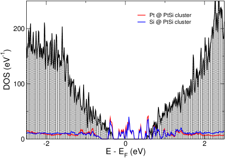
These results suggest that even a moderate supply of Pt atoms into a Si lattice would lead to the formation of PtSi clusters initially adopting the zincblende structure imposed by the host crystal. In order to test the validity of this conclusion for large numbers of Pt atoms, we considered a PtSi cluster with a diameter of approximately 1 nm, embedded in a 512-atom bulk Si supercell. In Fig. 2 we plot the density of states decomposed in the contributions from bulk Si atoms, and from Pt and Si atoms in the PtSi cluster. It can be seen that a complex structure of peaks appear in the Si band-gap, which reveals the metallic character of the cluster.
As the cluster grows in size, a phase transition to the bulk PtSi structure (favored by 0.55 eV/PtSi pair) is expected to occur. For this reason we have explicitly addressed the structural relaxation of a PtSi cluster of similar size with the thermodynamical stable structure, and we have found that for a cluster diameter of 1 nm relaxation to the host zincblende lattice is still thermodynamically favored.
We have also considered the formation of all-Pt clusters, examining both clusters where Pt adapts to the host zincblende symmetry or clusters where Pt takes the fcc symmetry of its bulk form. Although the formation energies of Pt or PtSi inclusions depend on the chemical potentials of the respective constituent species (which have a large degree of uncertainty), the differences in favor of PtSi clusters are so large that all-Pt clusters can be safely discarded.
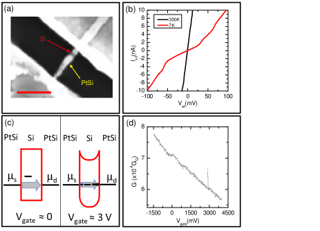
In the following we shall present experimental evidence for the existence of PtSi clusters in silicon devices with PtSi contacts. We shall investigate the effect of a single PtSi cluster on the transport properties of a short-channel transistor. PtSi/Si/PtSi SB transistors were fabricated from undoped silicon nanowires (NWs) with diameters in the nm range. The NWs were grown by chemical vapor deposition via a catalytic vapor-liquid-solid method Wagner and Ellis (1964). After growth, the NWs were transferred onto an oxidized silicon substrate and individually contacted by pairs of 80-nm-thick Pt electrodes deposited by sputtering (for more details on NW growth and device fabrication we refer the reader to refs. Gentile et al. (2008); Mongillo et al. (2011)). Each Pt electrode consisted of a 500-nm-wide and 3-m-long strip whose edges were connected to two Cr(10nm)/Au(65 nm) bonding pads via progressively wider Pt metal lines defined in the same deposition step. In order to promote the formation of PtSi contacts, the Pt strips were annealed one at a time by means of Joule effect. To this aim, an electrical current of 10 mA was sequentially applied through each Pt strip causing a local increase of the temperature and hence promoting the silicidation of the contacts. This silicidation technique, which was introduced and extensively discussed in Ref. Mongillo et al. (2011), was applied to obtain PtSi/Si/PtSi NW junctions with controlled Si channel length down to 10 nm (Fig.3(a)). Each NW junction was capped by a 5-nm-thick aluminium-oxide (Al2O3) layer, grown by Atomic Layer Deposition, and a Cr(10nm)/Au(60nm) top-gate electrode defined by e-beam lithography, metal evaporation, and lift-off.
Due to the absence of intentional doping and to the short channel length, the fabricated devices were found to operate as SB transistors Larson and Snyder (2006). In these transistors, the silicon channel is fully depleted. The conduction- and valence-band edges have essentially flat spatial profile (see Fig. 3( c), left panel) and their energy position relative to the Fermi levels of the PtSi contacts is set by the n- and p-type SBs, respectively. Since the p-type SB () is significantly smaller than the n-type SB (), electrical conduction is dominated by hole-type carriers.. Fig.3(b) shows the source-drain current, , as a function of source-drain bias voltage, , for two different temperatures. At room temperature (black trace) and for , transport through the silicon region is dominated by the thermionic emission of holes over the reverse-bias p-type SB. At 7 K (red trace), thermionic emission is entirely suppressed, and the residual conduction is due to temperature-independent tunneling through the silicon section, which acts as tunnel barrier Simmons (1963). A finite differential conductance, , is observed throughout the entire , thus including the linear regime around zero bias. The linear conductance, , decreases with the gate voltage, , as shown by the measurement in Fig.3(d), which was taken at 0.24 K. This p-type transistor behavior is characteristic of hole-dominated conduction. Once again, this follows from the fact that . An increase of causes a downward band bending in the silicon section leading to a higher tunnel barrier for holes (Fig. 3 (c)), and hence a lower conductance. Yet, due to a short-channel effect (the nanowire diameter is about four times the channel length), the gate effect is largely screened by the metallic PtSi contact. As a result, the exhibits a moderate modulation over the accessible gate-voltage range. In particular, remains finite up to the highest gate voltage applied (no higher voltages could be achieved due to the onset of significant gate leakage). A negative gate voltage produces an upward bending of the valence-band profile. Even for the largest , however, the valence-band edge remains well below the Fermi level of the contacts, such that no hole accumulation is induced in the silicon channel. This is consistent with the absence of Coulomb blockade behavior, which would be expected in concomitance with a gate-induced formation of a hole island in the silicon region (see, e.g., Ref. Zwanenburg et al. (2009)).
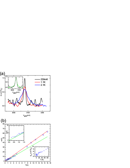
Interestingly, a sharp conductance peak is observed at a positive gate voltage close to 3 V, superimposed on the slowly varying background conductance. As shown in the inset to Fig. 4(a), following the subtraction of this background, the conductance peak can be fitted very well to a Lorentzian function Foxman et al. (1994); Beenakker (1991), revealing an underlying resonant-tunneling transport channel. The fitted peak width gives a measure of the tunnel coupling between the resonant state and the leads. The temperature dependence of the observed conductance resonance is shown in Fig. 4(a). As expected for resonant-tunneling, the conductance peak gets smaller and wider upon increasing temperature from 0.24 to a K. Above , the peak height increases again as shown in the lower inset of Fig. 4(b). On the contrary, , exhibits a monotonic temperature dependence as shown in Fig. 4(b)(main panel). To a closer look, however, is roughly constant below 0.6 K (see upper inset to Fig. 4(b)). In this low-temperature regime, the peak width is dominated by the life-time broadening of the resonant state due its tunnel coupling to the source and drain leads. Precisely, , where and are the tunnel rates to the source and drain contacts, respectively. Between 0.6 and 4 K, increases linearly with temperature according to the expectation for tunneling through a single discrete resonant level, i.e. ((Fig. 4(b), green line). This linewidth matches exactly the thermal broadening of the Fermi distribution function in the source and drain leads. A linear temperature dependence is observed also above 8 K, yet with a larger slope corresponding to the expectation for tunneling through an ensemble of closely spaced levels, i.e. (Fig. 4(b), red curve). Therefore, the crossover temperature K identifies the transition from quantum (single level) to classical (multiple levels) regime De Franceschi et al. (2003). This finding suggests that the observed conductance peak arises from resonant tunneling through a quantum dot with characteristic mean-level spacing .
To further support this conjecture we present in Fig. 5(a) a measurement of as a function of (,). The color plot (stability diagram) exhibits an X-shaped pattern which is typical for Coulomb-blockaded transport in quantum-dot systems Hanson et al. (2007); Kuemmeth et al. (2008). The crossing point, which corresponds to the conductance peak in the linear regime, represents the boundary between two consecutive Coulomb diamonds. In each diamond, transport through the quantum dot is blocked and the quantum dot hosts a well defined, integer charge state. Additional multiple lines parallel to the diamond edges can be seen in Fig. 5(a). Such types of lines are typical signatures of tunneling via the excited states of the quantum dot. Their positions relative to the diamond edges are set by the excitation energies of the corresponding quantum-dot states. The irregular spacing between the lines implies that the quantum-dot levels are not equally distributed in energy. Yet we can infer a characteristic mean-level spacing of the order of 1 meV, which is consistent with our earlier estimate based on the temperature dependence of the linear-conductance resonance.
The next step is to understand what kind of quantum dot could be responsible for the observed Coulomb-blockade features. Based on the gate dependence of Fig. 3(d) we already concluded that the silicon channel is fully depleted throughout the entire gate-voltage range. This allows us to rule out the possibility that the quantum dot is formed by confinement in the short silicon section. Thus we are left with the sole option of a Pt-based metallic nanocluster. Assuming that electrons in the nanocluster can be described to a good approximation as non interacting quasi-particles in spin degenerate levels von Delft and Ralph (2001), the mean-level spacing can be derived from the cluster diameter, , using the relation , where , and are the electron mass, metal Fermi wavevector and nanoparticle volume, respectively. From a level spacing of 1 meV, using m-1 , we find 4 nm. The data shown in Fig. 5(a) was focused on a narrow range around the observed tunnel resonance. From a similar measurement on a much larger () range (see Supplemental Material) we estimate a charging energy , which is consistent with a cluster diameter of a few nm.
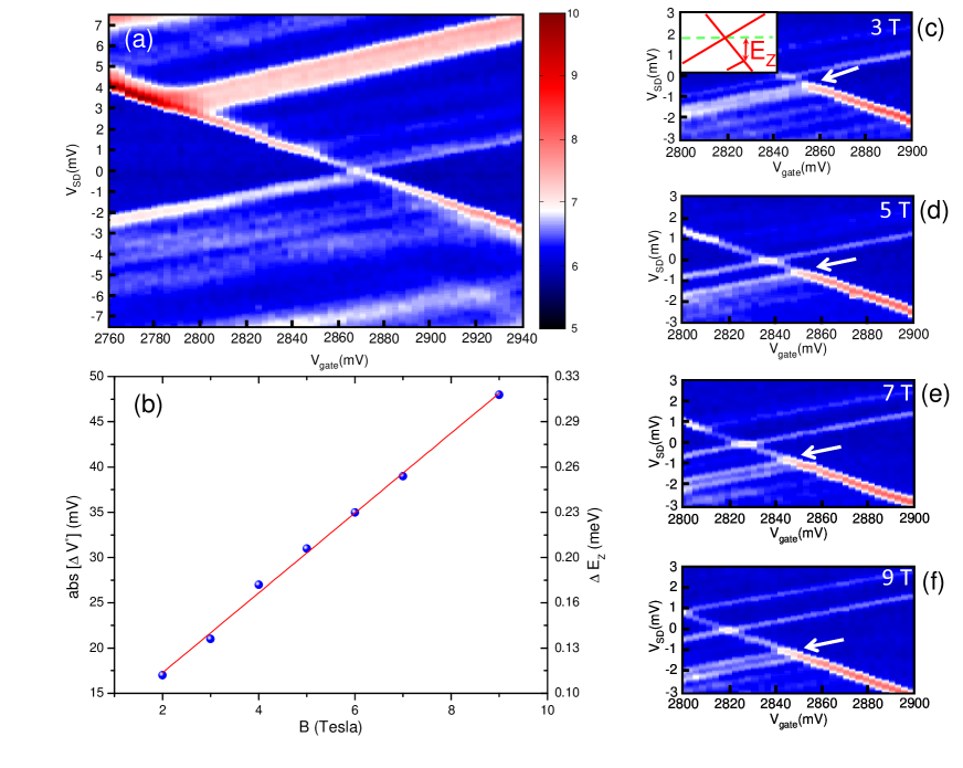
We now consider the effect of a magnetic field, , on the observed resonant level. Figure 5 (c)-(f) shows a set of stability diagrams measured at B = 3, 5, 7, and 9 T (in all these measurements B was applied perpendicularly to the substrate). We first note that by increasing B the X-shaped structure shifts progressively towards less positive values. This behavior can be ascribed to the Zeeman effect. To show that, let us label the gate-voltage position of the charge degeneracy point (i.e. the position of the resonance in the linear conductance) as ; then let us start with the hypothesis that the nanocluster has an even number of electrons and a spin for , and an odd number of electrons and S=1/2 for . Under this hypothesis, an applied magnetic field should result in a negative shift of proportional to the Zeeman energy shift of the spin-1/2 ground state.
Figure 5(b) shows the gate-voltage shift, as a function of . The dashed line is a linear fit to , where is a lever-arm parameter given by the ratio between the gate capacitance and the total capacitance of the cluster 222 is a conversion factor which relates the potential on the gate to the potential in the nanocluster, is the Bohr magneton, and is the electron g-factor, used as fitting parameter. The linear fit yields .
While the charge-degeneracy point undergoes a -induced leftward shift, the edges of the Coulomb diamond on its left are expected to split due to the removal of spin degeneracy. This effect is clearly seen on the lower diamond edge as highlithed by the white arrows in Figs. 5(c)-(f). The Zeeman energy can be directly measured from the position of the line associated to the excited spin state, as illustrated in the inset of Fig. 5(c). With this procedure we find , which is consistent with our previous estimate.
The fact that the measured g-factor coincides (within the experimental uncertainty) with the bare-electron value allows us to make some considerations about the nature of the quantum dot. To begin with, this finding constitutes further (indirect) evidence that the observed resonant channel cannot be associated with an isolated Pt impurity. In fact, valence electrons in Pt impurities are known to have anisotropic g-factors generally different from the bare-electron value Woodbury and Ludwig (1962); Anderson et al. (1991, 1992). This is because platinum is a heavy element with strong spin-orbit coupling. For the same reason, significant deviations of the g-factor from the bare-electron value have been observed in platinum metal structures Hjelm and Calais (1991) (and refs. therein), including Pt nanoclusters Liu et al. (2006) (we are aware of only one work Gordon and Marzke (1977) whose results do not agree with this trend). Therefore, our g-factor measurement provides an experimental indication against the hypothesis of a cluster consisting of pure platinum. The hypothesis of PtSi cluster, as suggested by our ab initio calculations, appears more plausible. With the aid of adequate numerical tools, it would be interesting to perform a calculation of the g-tensor in PtSi. Intuitively, one may indeed expect the g-factor to approach the bare electron value as a result of the considerable silicon content in the cluster. This tendency should be further reinforced by surface effects associated with the leakage of the electron wave-functions of surface atoms into the silicon host matrix van Leeuwen et al. (1994); Buttet et al. (1982); Hai et al. (2010).
In summary, through atomistic simulations and electronic transport measurements we have provided evidence of platinum clustering in silicon devices employing PtSi contacts. Our experiment on a short-channel PtSi/Si/PtSi SB transistor revealed the emergence at low temperature of a single-electron tunneling channel. This transport channel, which causes current resonances in the full-depletion (i.e. off) regime, is ascribed to a Pt-based metallic cluster embedded in the silicon section. Our atomistic simulations suggest the cluster to be most likely composed of PtSi. The cluster has discrete electronic levels with a characteristic energy spacing of 0.5 meV, corresponding to a diameter of a few nm, which is comparable to the characteristic length scales of the device. In addition, the cluster has a charging energy of 50 meV, which explains why single-electron effects survive up to relatively high temperatures. In the perspective of ultrascaled transistor devices, our study shows that the possible formation of PtSi clusters during the silicidation process can have important consequences on device performances. This issue can lead to significant device variability undermining the gain from using metal silicides and doping-free devices. Hence, we expect our results to have an impact in the engineering of a wide class of emerging electronic devices, including fully-depleted nano-transistors and ultra-fast PtSi Schottky barrier photodetectors.
Acknowledgements.
This work was supported by the Agence Nationale de la Recherche and by the EU through the ERC Starting Grant HybridNano . The authors would like to thank Laurent Cagnon Stephane Auffret and Xavier Waintal for technical support ans useful discussions.References
- Larson and Snyder (2006) J.M. Larson and J.P. Snyder, “Overview and status of metal s/d schottky-barrier mosfet technology,” Electron Devices, IEEE Transactions on, Electron Devices, IEEE Transactions on DOI - 10.1109/TED.2006.871842 53, 1048–1058 (2006).
- Dubois and Larrieu (2004) Emmanuel Dubois and Guilhem Larrieu, “Measurement of low schottky barrier heights applied to metallic source/drain metal–oxide–semiconductor field effect transistors,” J. Appl. Phys. 96, 729–737 (2004).
- Larrieu and Dubois (2011) G. Larrieu and E. Dubois, “Cmos inverter based on schottky source-drain mos technology with low-temperature dopant segregation,” Electron Device Letters, IEEE, Electron Device Letters, IEEE DOI - 10.1109/LED.2011.2131111 32, 728–730 (2011).
- Jang et al. (2005) Moongyu Jang, Yarkyeon Kim, Jaeheon Shin, and Seongjae Lee, “Characterization of erbium-silicided schottky diode junction,” Electron Device Letters, IEEE, Electron Device Letters, IEEE DOI - 10.1109/LED.2005.848074 26, 354–356 (2005).
- Zhu et al. (2004) Shiyang Zhu, Jingde Chen, M.-F. Li, S.J. Lee, J. Singh, C.X. Zhu, A. Du, C.H. Tung, A. Chin, and D.L. Kwong, “N-type schottky barrier source/drain mosfet using ytterbium silicide,” Electron Device Letters, IEEE, Electron Device Letters, IEEE DOI - 10.1109/LED.2004.831582 25, 565–567 (2004).
- Shigeyuki (1992) Uematsu Shigeyuki, “Infrared absorption and carrier generation in very thin ptsi film on p-type si crystal,” Vacuum 43, 1039–1041 (1992).
- Lin et al. (1995) T.L. Lin, J.S. Park, S.D. Gunapala, E.W. Jones, H.M. Del Castillo, M.M. Weeks, and P.W. Pellegrini, “7 m-cutoff ptsi infrared detector for high sensitivity mwir applications,” Electron Device Letters, IEEE, Electron Device Letters, IEEE DOI - 10.1109/55.363236 16, 94–96 (1995).
- Poate and Tisone (1974) J. M. Poate and T. C. Tisone, “Kinetics and mechanism of platinum silicide formation on silicon,” Appl. Phys. Lett. 24, 391–393 (1974).
- Asenov et al. (2003) A. Asenov, A.R. Brown, J.H. Davies, S. Kaya, and G. Slavcheva, “Simulation of intrinsic parameter fluctuations in decananometer and nanometer-scale mosfets,” Electron Devices, IEEE Transactions on, Electron Devices, IEEE Transactions on DOI - 10.1109/TED.2003.815862 50, 1837–1852 (2003).
- Lin et al. (2008) Yung-Chen Lin, Kuo-Chang Lu, Wen-Wei Wu, Jingwei Bai, Lih J. Chen, K. N. Tu, and Yu Huang, “Single crystalline ptsi nanowires, ptsi/si/ptsi nanowire heterostructures, and nanodevices,” Nano Letters 8, 913–918 (2008).
- Dellas et al. (2012-09-01) N. Dellas, C. Schuh, and S. Mohney, “Silicide formation in contacts to si nanowires,” (2012-09-01).
- Laszcz et al. (2006) A. Laszcz, J. Katcki, J. Ratajczak, A. Czerwinski, N. Breil, G. Larrieu, and E. Dubois, “Tem study of ptsi contact layers for low schottky barrier mosfets,” Si-based Materials for Advanced Microelectronic Devices: Synthesis, Defects and Diffusion Proceedings of the E-MRS IUMRS ICEM 2006 Spring Meeting - Symposium U: Si-based Materials for Advanced Microelectronic Devices: Synthesis, Defects and Diffusion E-MRS IUMRS ICEM 2006 Symposium U, Nuclear Instruments and Methods in Physics Research Section B: 253, 274–277 (2006).
- Liu et al. (2007) Bangzhi Liu, Yanfeng Wang, Sarah Dilts, Theresa S. Mayer, and Suzanne E. Mohney, “Silicidation of silicon nanowires by platinum,” Nano Letters 7, 818–824 (2007).
- Calvet et al. (2008a) L. E. Calvet, J. P. Snyder, and W. Wernsdorfer, “Excited-state spectroscopy of single pt atoms in si,” Phys. Rev. B 78, 195309– (2008a).
- Calvet et al. (2011) L. E. Calvet, J. P. Snyder, and W. Wernsdorfer, “Fano resonance in electron transport through single dopant atoms,” Phys. Rev. B 83, 205415– (2011).
- Calvet et al. (2008b) L. E. Calvet, W. Wernsdorfer, J. P. Snyder, and M.A Reed, “Transport spectroscopy of single pt impurities in silicon using schottky barrier mosfets,” J.Phys.:Condens. Matter 20, 374125–374129 (2008b).
- Mantovani et al. (1986) S. Mantovani, F. Nava, C. Nobili, and G. Ottaviani, “In-diffusion of pt in si from the ptsi/si interface,” Phys. Rev. B 33, 5536–5544 (1986).
- Prabhakar et al. (1983) A. Prabhakar, T. C. McGill, and M-A. Nicolet, “Platinum diffusion into silicon from ptsi,” Applied Physics Letters 43, 1118–1120 (1983).
- Watkins and Williams (1995) G. D. Watkins and P. M. Williams, “Vacancy model for substitutional ni-, pd-, pt-, and au0 in silicon,” Phys. Rev. B 52, 16575–16580 (1995).
- Anderson et al. (1991) F. G. Anderson, C. Delerue, M. Lannoo, and G. Allan, “Vacancy-model-based electronic structure of the pt- impurity in silicon,” Phys. Rev. B 44, 10925–10928 (1991).
- Anderson et al. (1992) Frederick G. Anderson, Frank S. Ham, and George D. Watkins, “Vacancy-model interpretation of epr spectrum of si:pt-,” Phys. Rev. B 45, 3287–3302 (1992).
- Woodbury and Ludwig (1962) H. H. Woodbury and G. W. Ludwig, “Spin resonance of pd and pt in silicon,” Phys. Rev. 126, 466–470 (1962).
- (23) Theoretical first-principles calculations have been performed within density-functional theory (DFT), as implemented in the Siesta package Soler et al. (2002); Ordejón et al. (1996). We have used an optimized double-basis set plus polarization functions for the valence electrons, while core electrons are accounted for by means of norm-conserving pseudopotentials of the Troullier-Martins type. The exchange-correlation energy is treated within the Generalized Gradient Approximation (GGA) Perdew et al. (1996). Pt point defects and 2- and 3-atom aggregates are studied n the supercell of the 8-atom bulk Si unit cell, while the 1 nm clusters were created in a larger supercell. The Brillouin zone was sampled with a grid of k-points, though a finer was used for an accurate determination of the densities of states in Fig.2. All the structures have been optimized until the force on the atoms were lower than 0.04 eV/Å.
- Note (1) For the sake of simplicity we are assuming that, in the slow-rate limit, Pt atoms reaches the clustering zone one by one. We believe, however, that this simplified model is enough to capture the physics of the aggregation process.
- Wagner and Ellis (1964) R. S. Wagner and W. C. Ellis, “Vapor-liquid-solid mechanism of single crystal growth,” Appl. Phys. Lett. 4, 89–90 (1964).
- Gentile et al. (2008) P. Gentile, T. David, F. Dhalluin, D. Buttard, N. Pauc, M. Den Hertog, P. Ferret, and T. Baron, “The growth of small diameter silicon nanowires to nanotrees,” Nanotechnology 19, 125608–125613 (2008).
- Mongillo et al. (2011) Massimo Mongillo, Panayotis Spathis, Georgios Katsaros, Pascal Gentile, Marc Sanquer, and Silvano De Franceschi, “Joule-assisted silicidation for short-channel silicon nanowire devices,” ACS Nano, ACS Nano 5, 7117–7123 (2011).
- Simmons (1963) John G. Simmons, “Generalized formula for the electric tunnel effect between similar electrodes separated by a thin insulating film,” J. Appl. Phys. 34, 1793–1803 (1963).
- Zwanenburg et al. (2009) Floris A. Zwanenburg, Cathalijn E. W. M. van Rijmenam, Ying Fang, Charles M. Lieber, and Leo P. Kouwenhoven, “Spin states of the first four holes in a silicon nanowire quantum dot,” Nano Letters 9, 1071–1079 (2009).
- Foxman et al. (1994) E. B. Foxman, U. Meirav, P. L. McEuen, M. A. Kastner, O. Klein, P. A. Belk, D. M. Abusch, and S. J. Wind, “Crossover from single-level to multilevel transport in artificial atoms,” Phys. Rev. B 50, 14193– (1994).
- Beenakker (1991) C. W. J. Beenakker, “Theory of coulomb-blockade oscillations in the conductance of a quantum dot,” Phys. Rev. B 44, 1646– (1991).
- De Franceschi et al. (2003) S. De Franceschi, J. A. van Dam, E. P. A. M. Bakkers, L. F. Feiner, L. Gurevich, and L. P. Kouwenhoven, “Single-electron tunneling in inp nanowires,” Appl. Phys. Lett. 83, 344–346 (2003).
- Hanson et al. (2007) R. Hanson, L. P. Kouwenhoven, J. R. Petta, S. Tarucha, and L. M. K. Vandersypen, “Spins in few-electron quantum dots,” Rev. Mod. Phys. 79, 1217–1265 (2007).
- Kuemmeth et al. (2008) Ferdinand Kuemmeth, Kirill I. Bolotin, Su-Fei Shi, and Daniel C. Ralph, “Measurement of discrete energy-level spectra in individual chemically synthesized gold nanoparticles,” Nano Letters, Nano Lett. 8, 4506–4512 (2008).
- von Delft and Ralph (2001) Jan von Delft and D.C. Ralph, “Spectroscopy of discrete energy levels in ultrasmall metallic grains,” Physics Reports 345, 61–173 (2001).
- Note (2) is a conversion factor which relates the potential on the gate to the potential in the nanocluster.
- Hjelm and Calais (1991) Anders Hjelm and Jean-Louis Calais, “Zeeman splitting in pd and pt calculated from self-consistent band structure including an external magnetic field,” Phys. Rev. Lett. 67, 2064–2067 (1991).
- Liu et al. (2006) X. Liu, H. Dilger, R. A. Eichel, J. Kunstmann, and E. Roduner, “A small paramagnetic platinum cluster in an nay zeolite: characterization and hydrogen adsorption and desorption,” The Journal of Physical Chemistry B, J. Phys. Chem. B 110, 2013–2023 (2006).
- Gordon and Marzke (1977) D. A.. Gordon and W. S. Marzke, R. F.and Glaunsinger, “Size distribution and esr of uniform microcrystal of platinum,” Journal de Physique (Paris) Colloques 38, 87–92 (1977).
- van Leeuwen et al. (1994) David A. van Leeuwen, J. M. van Ruitenbeek, L. J. de Jongh, A. Ceriotti, G. Pacchioni, O. D. Häberlen, and N. Rösch, “Quenching of magnetic moments by ligand-metal interactions in nanosized magnetic metal clusters,” Phys. Rev. Lett. 73, 1432–1435 (1994).
- Buttet et al. (1982) J. Buttet, R. Car, and Charles W. Myles, “Size dependence of the conduction-electron-spin-resonance g shift in a small sodium particle: Orthogonalized standing-wave calculations,” Phys. Rev. B 26, 2414–2431 (1982).
- Hai et al. (2010) Pham Nam Hai, Shinobu Ohya, and Masaaki Tanaka, “Long spin-relaxation time in a single metal nanoparticle,” Nat Nano 5, 593–596 (2010).
- Soler et al. (2002) José M Soler, Emilio Artacho, Julian D Gale, Alberto García, Javier Junquera, Pablo Ordejón, and Daniel Sánchez-Portal, “The siesta method for ab initio order- n materials simulation,” J. Phys.: Condens. Matter 14, 2745–2779 (2002).
- Ordejón et al. (1996) Pablo Ordejón, Emilio Artacho, and José M. Soler, “Self-consistent order- density-functional calculations for very large systems,” Phys. Rev. B 53, R10441–R10444 (1996).
- Perdew et al. (1996) John P. Perdew, Kieron Burke, and Matthias Ernzerhof, “Generalized gradient approximation made simple,” Phys. Rev. Lett. 77, 3865–3868 (1996).