Externally controlled local magnetic field in a conducting mesoscopic ring coupled to a quantum wire
Abstract
In the present work the possibility of regulating local magnetic field in a quantum ring is investigated theoretically. The ring is coupled to a quantum wire and subjected to an in-plane electric field. Under a finite bias voltage across the wire a net circulating current is established in the ring which produces a strong magnetic field at its centre. This magnetic field can be tuned externally in a wide range by regulating the in-plane electric field, and thus, our present system can be utilized to control magnetic field at a specific region. The feasibility of this quantum system in designing spin-based quantum devices is also analyzed.
pacs:
73.23.-b, 73.23.Ra, 85.35.DsI Introduction
The phenomenon of voltage driven circular currents in conducting junctions with single or multiple loop substructures is a notable quantum effect in low-dimensional systems. Most of the studies involving electron transport through different bridge systems essentially focus on net current transfer orella1 ; orella2 ; tagami ; ventra2 ; ventra1 ; aviram ; nitzan1 ; skm1 ; skm2 ; walc ; woi ; skm3 ; skm4 ; skm5 ; skm6 rather than analyzing current distribution among different branches dist2 ; dist3 ; dist1 of the materials within the junction. In last few years, some interesting works have been done considering different molecular structures where distribution of currents in different arms has been analyzed providing the possibilities of getting voltage induced circular currents cir5 ; cir4 ; cir1 ; cir2 ; cir3 . These circular currents produce substantial magnetic fields at ring centre and can be exploited in many ways to explain several interesting quantum mechanical phenomena as well as to design quantum devices for future applications.
Controlling of a single spin placed at or near the centre of a ring-shaped geometry by means of magnetic field associated with circular currents may be the most suitable application towards this direction, since proper spin control is extremely important in designing spin-based quantum devices dev1 ; dev2 ; dev3 ; dev4 . Nowadays people are highly focused in computing with single electron spin since it involves much lower power dissipation rather than traditional computing which is always charge based. In traditional computing, computable informations are encoded by electrical charge which has only a magnitude but no direction i.e., a scalar quantity. Thus, to encode binary logic bits and using electrical charge two different amounts of charge are required. Now, if the bit is switched the magnitude of the charge required to encode logic levels should be changed, and accordingly, a net current flow takes place. This net current flow certainly produces a power loss. On the other hand, if computable informations are encoded by using spin, which is a pseudovector, then the bits and can be described by up and down spin configurations, respectively. In this case the switching between two bits can be associated with the flipping of the spin without transferring any net charge and thus much lower power dissipation can be achieved.
In order to design spin-based quantum devices proper control of magnetic field at a particular point is highly important. Till now very few attempts have been made to get controlled magnetic field in some particular region considering some quantum systems for possible spintronics applications.
For example, in 2003 Cho et al. cho have proposed a double quantum dot (QD) system which can act as a magnetically polarized device when coherent electrons circulate through closed path of the dots and side attached electrodes. It has been shown that manipulating the energy level position of each dot, the double QD device can be magnetized as up-, down- or non-polarized. In presence of a finite bias, this system exhibits a circular current and reaches a maximum of nA. In the subsequent year Lidar et al. lidar have established a new method to produce exponentially decaying magnetic field using an array of current-carrying wires where the neighboring wires carry currents in opposite directions. They have produced a peak magnetic field of mT. The major issue of this setup is the heating effect and it has been examined that the system works well when the system temperature mK. Such a small temperature can be substantiated with dilution refrigeration technology. In other work, Pershin et al. have shown how to create magnetic field at a specific region of an isolated semi-conducting quantum ring using phase-locked infrared laser pulses pershin . Here, the induced magnetic field is controlled by laser pulses and the estimated magnetic field at the ring center is of the order of mT, comparable to the result obtained in Ref. lidar . Later, in 2012 Anda et al. anda have presented a system constituted by two QDs embedded in a metallic ring coupled to external electrodes in which the possibility of controlling circulating currents by means of external gate potential has been analyzed. This system could be utilized to regulate circular current induced magnetic field, but this aspect has not been addressed anywhere in their work. Therefore, it can be usually asked that how much magnetic field will be established at the center of this ring and how it varies with external gate potential? Also the feasibility of utilizing this system to design a spin-based quantum device has not been discussed.
Though few works are available in this particular area, still several important issues are unexplored. For example (i) designing of a simple quantum system that can produce strong enough circular current, (ii) generation of a strong magnetic field at a particular region, and (iii) control of this magnetic field in a wide variable range. Simultaneously, the usefulness of the system even at moderate temperature is also an important issue. To the best of our knowledge these features are unaddressed so far, and, in the present work we essentially focus towards this direction. Here, we describe a new technique to control magnetic field externally in a conducting quantum ring (QR) which is coupled to a quantum wire (QW) and subjected to an in-plane electric field. Under a finite bias voltage a net circulating current is established in the ring and it produces a strong magnetic field at its centre. This magnetic field can be regulated by tuning the in-plane electric field without directly changing other physical parameter of the model considered. From our analysis we will show that the induced magnetic field can be varied in a wide range starting from zero to several milliTesla with the help of external in-plane electric field.
The phenomenon of circulating current in a conducting ring has already been established few decades ago in another context pc1 ; pc2 ; pc3 ; pc4 ; pc5 ; pc6 ; pc66 ; pc7 ; pc8 where current is induced by Aharonov-Bohm (AB) flux . This circularly current, the so-called persistent current, in AB ring is quite different in origin compared to the circulating currents in conducting junctions where current is driven by applied voltage bias. In presence of a finite bias, a net circulating current can be obtained in a loop geometry even in the absence of any AB flux .
We organize the paper as follows. In Section II we describe the model together with theoretical formulations for the calculations. Essential results are described in Section III, which include the variation of internal current distribution, effects of system sizes and other physical parameters on circular current and associated magnetic field, and the feasibility condition for practical realizations. Finally, we summarize our findings in Section IV.
II Model and theoretical framework
II.1 Tight-binding model
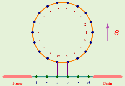
Our system comprises a quantum ring which is coupled to a quantum wire and subjected to an in-plane electric field perpendicular to the wire. The wire is attached to two semi-infinite one-dimensional metal electrodes, usually known as source and drain. The schematic diagram of our system is presented in Fig. 1. In order to get a non-vanishing circular current in the ring, we couple it to the wire through two vertical bonds. No net current will be obtained in the ring if it is connected to the wire via single vertical bond due to mutual cancellation of currents moving clockwise and anti-clockwise directions.
We use a tight-binding framework to describe the model which is extremely suitable for describing electron transport through a conducting junction especially for the case where electron-electron interaction is not taken into account. The single particle tight-binding Hamiltonian that involves the ring, wire and side-attached electrodes can be written as,
| (1) |
where, , and correspond to different sub-Hamiltonians those are described as follows. The first term corresponds to the Hamiltonian of the conductor bridging the two electrodes i.e., the ring with coupled quantum wire. Under nearest-neighbor hopping approximation the Hamiltonian gets the form,
| (2) | |||||
where, and represent the creation and annihilation operators of an electron at -th site of the QR, while for the QW these operators are represented by and , respectively. The ring is parametrized by on-site energy and nearest-neighbor hopping integral , and similarly we parametrize the wire by the terms and . measures the coupling between the QR and QW, where they are coupled through the lattice sites , , and (see Fig. 1), those are variable.
Now, in presence of an in-plane electric field which is perpendicular to the wire, the site energy of the QR becomes field dependent. For a -site ring it becomes: , where corresponds to the electronic charge, represents the lattice spacing and measures the strength of the in-plane electric field. This field dependent site energy relation is again simplified by introducing the dimensionless electric field strength and can be written as , where . In our formulation, we use the parameter to describe the system size of the QW.
The second term in Eq. 1 corresponds to the Hamiltonian of one-dimensional source and drain electrodes. It is expressed as
where, presents the on-site energy and gives the nearest-neighbor hopping strength in the electrodes. For a -th site electron in these electrodes the creation and annihilation operators are described by and , respectively.
Finally, the third term in Eq. 1 denotes the coupling of the wire to the source and drain electrodes. Considering and are coupling integrals between the wire and side-attached electrodes, the Hamiltonian can be written as,
| (4) | |||||
II.2 Circular current in the QR
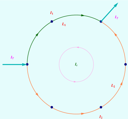
To determine circular current in the system considered let us first focus on the current distribution in a simple model where a mesoscopic ring is coupled to two electrodes (see Fig. 2). A net junction current flows between source and drain, where and are the currents propagating through upper and lower arms of the ring, respectively. For the current flowing in the counter-clockwise direction we use positive sign, while it is negative for the other direction. Following the current distribution given in Fig. 2, the net circulating current in the ring is defined as cir1 ,
| (5) |
where, . and are the arm lengths. This is the basic definition of circular current in any loop geometry attached to two electrodes. The relation, Eq. 5, immediately suggests that for a symmetrically connected ring no net circular current will appear since in this case and . Now to calculate using Eq. 5, we have to determine currents in different segments of the ring geometry. We compute these currents using Green’s function formalism. At absolute zero temperature (T=K), current in a bond connecting the sites and , where , can be expressed as,
| (6) |
is the charge current density and it provides a net bond current upon integrating over a particular energy window. is the equilibrium
Fermi energy and is the applied bias voltage between source and drain electrodes. To describe current density we impose correlation Green’s function and in terms of it, can be written as dist3
| (7) |
The correlation Green’s function is defined in the form: , where and are the retarded and advanced Green’s functions, respectively, and they obey the relation . is the coupling matrix associated with the coupling of the conductor to the source electrode. Introducing the concept of contact self-energies and due to two semi-infinite one-dimensional electrodes we can write datta ,
| (8) |
where, is the energy of an injecting electron. During evaluation of the correlation function we fix the occupation function of the source electrode to unity while for the drain electrode it becomes zero.
II.3 Magnetic field in the QR associated with circular current
Due to circular current , a net magnetic field is established in the ring. At any point inside the ring, we calculate the magnetic field by using Biot-Savart’s law which looks like cir1 ,
| (9) |
where, is the position vector for the bond current element and is the magnetic constant.
Throughout the results discussed below in Sec. III, unless otherwise stated, we fix the electronic temperature to zero and assume that the entire voltage is dropped at the wire-to-electrode interfaces. The other common parameters are as follows: , eV, eV, and eV. The lattice spacing and the equilibrium Fermi energy is set at zero.
III Numerical results and discussion
Based on the above theoretical framework we are now ready to present our numerical results for circular currents and associated magnetic fields, and the effect of in-plane electric field on them. These results are described in different sub-sections as follows.
III.1 Internal current distribution
Before focusing to the central problem i.e., the possibility of controlling local magnetic field associated with voltage induced circular current by means of external electric field, without directly changing other system parameters, we start with the current distribution shown in Fig. 3. A net junction current flowing from the source to drain electrode is distributed among different branches of the bridge setup where distinct colored arrows correspond to different magnitudes of the bond currents. These bond currents are determined when the bias voltage is fixed at V and the dimensionless electric field strength is set equal to . In this setup we consider a -site ring so that the upper arm contains identical bonds, while only a single bond exists in the lower arm, and the currents in these two arms with unequal magnitudes associated with the voltage bias are propagating in a particular direction (anti-clockwise) which result a non-vanishing circular current in the ring. For a finite bias, the direction of these bond currents strongly influenced by the way the QR is coupled to the QW. In our chosen configuration, illustrated in Fig. 3, two neighboring atomic sites of the ring are coupled to the wire such that the difference () between the arm lengths becomes maximum. With reducing this length difference, oppositely rotating bond currents in the upper and lower arms of the QR can be obtained depending on the voltage window, and eventually when currents with exactly equal in magnitude are available in the upper and lower arms of the ring those propagate in reverse directions irrespective of the choice of the voltage bias which provide a vanishing circular current in the QR. The phenomenon of voltage driven circular current in a conducting loop can be
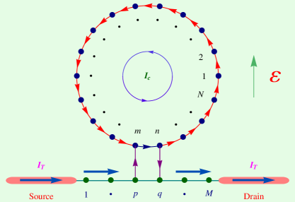
explained in terms of current carrying states associated with energy eigenvalues of the system. For a finite voltage bias when a single resonating state lies within the voltage window circulating current is obtained due to this particular state and the direction of this current is also governed by it. On the other hand, when more resonating states those carry currents in opposite directions appear within the voltage regime, then all of them contribute to the current and a resultant is obtained. Certainly, the sign of the net current depends on the dominating states i.e., the states contributing more to the current than the others.
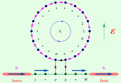
Like the voltage bias and the ring-to-wire configuration (), nature of these bond currents is also affected noticeably by the other physical parameters of the system. To substantiate it, in Fig. 4 we present the variation of current distribution in individual branches of the same bridge configuration as taken in Fig. 3, except that and eV. Under this situation oppositely rotating currents with unequal magnitudes are available even when is maximum, and, depending on the branch currents a net circulating current is established in the QR.
III.2 Circular current and associated magnetic field for different system sizes
Following the above features of current distribution among different branches we can now move to demonstrate the characteristic features of circular current and associated magnetic field as a function of
voltage bias, and, the effect of in-plane electric field on these quantities for different system sizes.
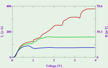
As representative example, in Fig. 5 we present the variation of circular current (left axis) and the associated magnetic field (right axis) at the ring centre considering and . The results are computed for three distinct values of the dimensionless electric field strength , those are illustrated by three different colored curves. Several interesting features are observed. First, in the absence of in-plane electric field a very large circulating current (red line) is obtained in the QR and it gradually increases with the bias voltage and reaching a maximum of . The current also exhibits some tiny oscillations with the applied bias. Second, the associated magnetic field at the ring center induced by the circular current is considerably large and reaches to mT. This is reasonably high compared to the previous studies of externally controlled magnetic field at a particular region where local magnetic field is generated either by using laser-controlled approach pershin or with the help of arrays of parallel current-carrying wires lidar or using double QD device cho . Finally, both the circular current and induced magnetic field decrease with increasing dimensionless electric field strength , and, for a wide voltage regime they are almost constant.
The above three features can be physically understood as follows. As discussed in the previous sub-section we note that the circular current for a particular bias is a resultant contribution of all the states carrying currents those come into the voltage window. Therefore, with increasing external bias more and more resonating states appear and all of them contribute to the current which finally yield a larger circular current. Obviously, a strong magnetic field is obtained at the ring center
associated with this large current . The reduction of the circular current as well as the induced magnetic field in presence of in-plane electric field can be illustrated by considering the QR as a disordered one. In the absence of any in-plane electric field site energies of the QR are equal ( ) which make the ring as a perfect one. Whereas, for finite electric field () these site energies are field dependent and they are no longer identical with each other which provide a disordered QR. Under this situation the current carrying states are not as much extended like the electric field free case () and hence reduced circular current is obtained. Accordingly, we also get less magnetic field at the ring center. With increasing electric field strength both the circular current and magnetic field get reduced which can be detected from the curves shown in Fig. 5. More clear picture of this field dependence on circular current and associated magnetic field is discussed in a separate sub-section (sub-section D) below. In addition to the above facts it is also interesting to note that for non-zero electric field the circular current gradually increases with external bias in a relatively narrow voltage region, while the rate of increment sharply decreases in the higher voltage regimes (see the green and blue lines in Fig. 5). The reason is that in the weak voltage regions, resonant states contribute significantly differently which result a net larger current, while the difference gets reduced slowly with higher voltage regions associated with the split
energylevels and hence almost constant current is generated. Finally, the behavior of tiny oscillations in circular current can be elucidated in terms of the discreteness of resonating energy eigenstates for the finite size systems. The bond current is obtained by integrating the charge current density (see Eq. 6) over a particular voltage window where finite resonant states contribute to the current. In the absence of electric field, sharp resonant states are obtained since the QR behaves like an impurity-free ring which generate tiny oscillating current in the integration procedure, while in the case of finite electric field much broader resonant energy levels arise as the QR is treated as a disordered one and a less oscillating current appears.
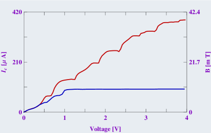
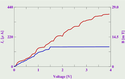
Observations of circular current and associated magnetic field with other sizes of the QR and QW are qualitatively similar to those with the bridge setup where we set and (Fig. 5). The results are shown in Figs. 6 and 7 for different strengths of the dimensionless electric field . In Fig. 6 we set and , while in Fig. 7 we choose and . Comparing the spectra shown in Figs. 5-7 we emphasize that the results are quite robust and can be utilized to generate strong circular current as well as magnetic field.
III.3 Effect of on circular current and magnetic field
In order to substantiate the effect of ring-to-wire coupling () on circular current and associated magnetic field induced by this current, in Fig. 8 we present the results for a -site ring considering different values of . The results are computed setting the dimensionless electric field strength , where the red, green and blue lines correspond to eV, eV and eV, respectively.
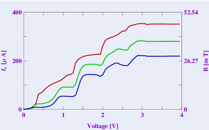
From the spectra it is observed that the circular current and its associated magnetic field get slightly reduced with increasing the ring-to-wire coupling strength, though all the other features remain qualitatively similar as discussed earlier.
III.4 Circular current and magnetic field versus electric field characteristics
The results presented so far to regulate circular current induced magnetic field at the ring center by means of external in-plane electric field are computed for some typical field strengths. To have a fine tuning of local magnetic field at ring center with the help of external electric field, now we focus our attention on the results shown in Fig. 9. Here we demonstrate the behavior of circular current (left axis) and induced magnetic field (right axis) as a function of dimensionless electric field strength considering and . The results are shown for two different bias voltages, where the red and blue curves correspond to V and V, respectively. Quite interestingly we find that both circular current and the corresponding magnetic field decrease monotonically with increasing the strength of the electric field. This reduction can be easily justified from our previous discussion where the QR is treated as a disordered one in presence of the electric field. Certainly, the ring becomes more disordered with increasing the field strength which results more reduced current, and eventually, it drops to zero for strong field strength.
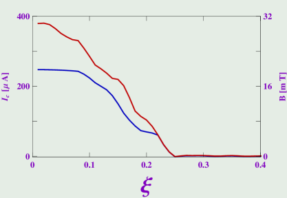
Our results clearly suggest that the magnetic field at the ring centre can be well adjusted by tuning the external electric field, and thus, our proposed quantum system can be used as an externally controlled source of local magnetic field.
III.5 Practicability consideration and technological importance
Finally, we discuss the applicability of this quantum system to develop spin-based quantum devices. To get it feasible, first it is important to calculate the required magnetic field for a single-qubit operation. It is well known that magnetic field can able to change the alignment of a single spin. To rotate a single spin by a relative angle for a time scale the required magnetic field is given by lidar : , where is the -factor and is the Bohr magneton. Assuming the average operation time lidar ns, the desired magnetic field for rotating the spin by an angle is mT.
For the present system we find that the induced magnetic field at the ring centre is quite high compared to the above estimated magnetic field to rotate a single spin by an angle . In addition to this, we also establish that the magnetic field induced by circular current can be well controlled and varied in a wide range starting from zero to several milliTesla (mT) by means of external in-plane electric field, without directly disturbing other physical parameters of the system. Our results clearly suggest that in all respects the present quantum system is technologically feasible and can be utilized to design spin-based quantum devices.
IV Conclusion
To conclude, in the present work, we have demonstrated one possible route of controlling local magnetic field at a particular point externally without disturbing the system parameters. Our system comprises a quantum ring which is directly coupled to a quantum wire under a specific configuration. The ring is subjected to an in-plane electric field and it is the key controlling parameter of our present study. In presence of a finite bias voltage across the two ends of the quantum wire, a net circulating current appears in the ring, and accordingly, a magnetic field is established at its centre. Changing the in-plane electric field and keeping all other parameters unchanged, the magnetic field at the ring centre can be adjusted in a tunable way. We have employed a simple tight-binding framework to illustrate the quantum system and calculated all the results using Green’s function formalism. Our presented results undoubtedly suggest that the system can be utilized as a source of local magnetic field that can be controlled externally. Finally, we have also discussed about the feasibility of our quantum system in designing spin-based quantum devices. We have established that the induced magnetic field at the ring center can be varied in a wide range with the help of external in-plane electric field which is highly significant in the present era of spintronic applications. We strongly believe that the present investigation provides a much simpler way of controlling local magnetic field in such a broader range than the conventional techniques lidar ; pershin .
Some valid approximations have been taken into account in this study. The first one is the zero temperature approximation. Here we have computed the results considering zero temperature limit, but these results are equally valid even at finite temperatures since thermal broadening of the energy levels of the bridging system is much weaker than the broadening caused by the wire-to-electrode coupling datta ; br1 ; br2 ; br3 . To have a quantitative estimate we calculate average spacing of the energy levels of the bridging system which is eV, and it is reasonably high compared to the thermal energy eV in the room temperature () limit. Thus, our predicted results fit reasonably well at moderate temperatures. The other approximation is the consideration of non-interacting electron picture. In presence of electron-electron interaction ee1 ; ee2 ; ee3 one might expect some interesting patterns, but all the physical phenomena analyzed here will remain unchanged. Beside these we have also ignored the effects of electron dephasing dp1 ; dp2 ; dp3 ; dp4 , system impurities dis1 ; dis2 , etc. These issues will be addressed elsewhere in our future work.
Finally, it is important to note that during the numerical calculations we have taken some specific parameter values to compute the results, but all the physical properties studied here remain absolutely invariant for other choices of the parameter values, which essentially suggests the robustness of our investigation. Our results certainly demand an experimental verification in this line.
References
- (1) P. Orellana and F. Claro, Phys. Rev. Lett. 90, 178302 (2003).
- (2) J. H. Ojeda, R. P. A. Lima, F. Domínguez-Adame, and P. A. Orellana, J. Phys.: Condens. Matter 21, 285105 (2009).
- (3) K. Tagami, L. Wang, and M. Tsukada, Nano Lett. 4, 209 (2004).
- (4) M. D. Ventra, N. D. Lang, and S. T. Pentelides, Chem. Phys. 281, 189 (2002).
- (5) M. D. Ventra, S. T. Pentelides, and N. D. Lang, Appl. Phys. Lett. 76, 3448 (2000).
- (6) A. Aviram and M. Ratner, Chem. Phys. Lett. 29, 277 (1974).
- (7) A. Nitzan and M. A. Ratner, Science 300, 1384 (2003).
- (8) S. K. Maiti, Solid State Commun. 150, 1269 (2010).
- (9) S. K. Maiti, J. Nanosci. Nanotechnol. 8, 4096 (2008).
- (10) K. Walczak, Cent. Eur. J. Chem. 2, 524 (2004).
- (11) S. Woitellier, J. P. Launay, and C. Joachim, Chem. Phys. 131, 481 (1989).
- (12) P. Dutta, S. K. Maiti, and S. N. Karmakar, Org. Electron. 11, 1120 (2010).
- (13) S. K. Maiti, Org. Electron. 8, 575 (2007).
- (14) S. Sil, S. K. Maiti, and A. Chakrabarti, Phys. Rev. B 78, 113103 (2008).
- (15) M. Dey, S. K. Maiti, and S. N. Karmakar, Eur. Phys. J. B 80, 105 (2011).
- (16) S. Nakanishi and M. Tsukada, Surf. Sci. 438, 305 (1999).
- (17) L. Wang, K. Tagami, and M. Tsukada, Jpn. J. Appl. Phys. 43, 2779 (2004).
- (18) M. Tsukada, K. Tagami, K. Hirose, and N. Kobayashi, J. Phys. Soc. Jpn. 74, 1079 (2005).
- (19) K. Tagami and M. Tsukada, Curr. Appl. Phys. 3, 439 (2003).
- (20) G. Stefanucci, E. Perfetto, S. Bellucci, and M. Cini, Phys. Rev. B 79, 073406 (2009).
- (21) D. Rai, O. Hod, and A. Nitzan, J. Phys. Chem. C 114, 20583 (2010).
- (22) S. K. Maiti, Eur. Phys. J. B 86, 296 (2013).
- (23) D. Rai, O. Hod, and A. Nitzan, Phys. Rev. B 85, 155440 (2012).
- (24) B. E. Kane, Nature (London) 393, 133 (1998).
- (25) V. Privman, I. D. Vagner, and G. Kventsel, Phys. Lett. A 239, 141 (1998).
- (26) G. Burkard, D. Loss, and D. P. DiVincenzo, Phys. Rev. B 59, 2070 (1999).
- (27) Yu. V. Pershin, I. D. Vagner, and P. Wyder, J. Phys.: Condens. Matter 15, 997 (2003).
- (28) S. Y. Cho, R. H. McKenzie, K. Kang, and C. K. Kim, J. Phys.: Condens. Matter 15, 1147 (2003).
- (29) D. A. Lidar and J. H. Thywissen, J. Appl. Phys. 96, 754 (2004).
- (30) Yu. V. Pershin and C. Piermarocchi, Phys. Rev. B 72, 245331 (2005).
- (31) E. V. Anda, G. Chiappe, and E. Louis, J. Appl. Phys. 111, 033711 (2012).
- (32) M. Büttiker, Y. Imry, and R. Landauer, Phys. Lett. A 96, 365 (1983).
- (33) H. F. Cheung, Y. Gefen, E. K. Reidel, and W. H. Shih, Phys. Rev. B 37, 6050 (1988).
- (34) L. P. Levy, G. Dolan, J. Dunsmuir, and H. Bouchiat, Phys. Rev. Lett. 64, 2074 (1990).
- (35) P. A. Orellana, M. L. Ladrón de Guevara, M. Pacheco, and A. Latgé, Phys. Rev. B 68, 195321 (2003).
- (36) S. K. Maiti, J. Chowdhury, and S. N. Karmakar, Phys. Lett. A 332, 497 (2004).
- (37) S. K. Maiti, J. Chowdhury and S. N. Karmakar, J. Phys.: Condens Matter 18, 5349 (2006).
- (38) S. K. Maiti, J. Chowdhury and S. N. Karmakar, Solid State Commun. 135, 278 (2005).
- (39) S. K. Maiti, Int. J. Mod. Phys. B 21, 179 (2007).
- (40) S. K. Maiti, M. Dey, S. Sil, A. Chakrabarti, and S. N. Karmakar, Europhys. Lett. 95, 57008 (2011).
- (41) S. Datta, Electronic transport in mesoscopic systems, Cambridge University Press, Cambridge (1997).
- (42) S. K. Maiti, Solid State Commun. 149, 1623 (2009).
- (43) S. K. Maiti, Physica B 394, 33 (2007).
- (44) S. K. Maiti, Physica E 36, 199 (2007).
- (45) H. Kato and D. Yoshioka, Phys. Rev. B 50, 4943 (1994).
- (46) A. Kambili, C. J. Lambert, and J. H. Jefferson, Phys. Rev. B 60, 7684 (1999).
- (47) S. K. Maiti and A. Chakrabarti, Phys. Rev. B 82, 184201 (2010).
- (48) M. Büttiker, Phys. Rev. B 33, 3020 (1986).
- (49) M. Büttiker, IBM J. Res. Dev. 32, 63 (1988).
- (50) R. Golizadeh-Mojarad and S. Datta, Phys. Rev. B 75, 081301(R) (2007).
- (51) M. Dey, S. K. Maiti, and S. N. Karmakar, Org. Electron. 12, 1017 (2011).
- (52) S. K. Maiti, Solid State Commun. 150, 2212 (2010).
- (53) S. K. Maiti, Phys. Status Solidi B 248, 1933 (2011).