Proximity nanovalve with large phase-tunable thermal conductance
Abstract
We propose a phase-controlled heat-flux quantum valve based on the proximity effect driven by a superconducting quantum interference proximity transistor (SQUIPT). Its operation relies on the phase-dependent quasiparticle density of states in the Josephson weak-link of the SQUIPT which controls thermal transport across the device. In a realistic Al/Cu-based setup the structure can provide efficient control of thermal current inducing temperature swings exceeding mK, and flux-to-temperature transfer coefficients up to mK/ below 100 mK. The nanovalve performances improve by lowering the bath temperature, making the proposed structure a promising building-block for the implementation of coherent caloritronic devices operating below 1 K.
Phase-dependent manipulation of heat in solid-state nanodevices is nowadays one of the major challenges of coherent caloritronics Martínez-Pérez et al. (2014), and plays a key role in determining the physical properties of mesoscopic systems at low temperature. Toward this direction, the prototype for a heat interferometer has been recently realized with a superconducting quantum interference device (SQUID) where the modulation of the thermal current has been achieved thanks to the Josephson coupling Giazotto and Martínez-Pérez (2012a, b); Martínez-Pérez and Giazotto (2013, 2014). Yet, phase-dependent thermal transport has been also demonstrated in Andreev interferometers Eom et al. (1998); Dikin et al. (2001); Bezuglyi and Vinokur (2003) where the proximity effect in a normal metal affects its thermal conductance, and is controlled via a magnetic field.
Here we propose an alternative approach to control heat transport by envisioning a thermal nanovalve based on proximity effect but phase-controlled by a SQUIPT Giazotto et al. (2010); Meschke et al. (2011); Jabdaraghi et al. (2014); Ronzani et al. (2014). Differing from SQUID-based and Andreev interferometers our device allows a drastic quenching of the thermal conductance which makes our proposal an efficient phase-tunable thermal nanovalve. Specifically, we expect an improvement of the temperature swing (up to mK) and a flux-to-temperature transfer function exceeding 500 mK at 100 mK.
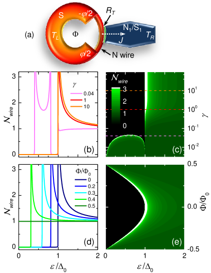
A sketch for the proximity nanovalve is shown in Fig. 1(a) and consists of a SQUIPT composed by a superconducting (S) ring interrupted by a diffusive normal metal (N) wire of length . We assume the wire transverse dimensions to be negligible in comparison to its length so that it can be considered as quasi-one-dimensional. Superconducting correlations are induced in the N wire owing to proximity effect from the S loop which modifies the wire density of states (DoS) Guéron et al. (1996). In addition, a normal metal (N1) or a superconducting electrode (S1) identical to S is tunnel-coupled to the middle of the wire through an insulating contact of negligible width respect to the wire length. denotes the normal-state resistance of the junction. We assume the SN ring and the N1(or S1) electrode to be in steady-state thermal equilibrium and to reside at different temperatures and , respectively, with . The nanovalve is therefore only temperature biased. In the limit of negligible geometric inductance of the ring it follows that , where is the phase difference across the SN boundaries, is the applied magnetic flux through the loop, and Wb is the flux quantum. The ring geometry allows to change which leads to the modification of the N-wire DoS Zhou et al. (1998) and, in turn, a drastic modification of thermal transport through the device.
The DoS in the N wire () is given by where is the normal retarded quasiclassical Green’s function, is the energy, and is the spatial coordinate along the wire. The function can be obtained by solving the one-dimensional Usadel equation (we skip the supra index ) Usadel (1970)
| (1) |
where is the wire diffusion coefficient, the parameter accounts for the inelastic scattering rate within the relaxation time approximation Dynes et al. (1984); Pekola et al. (2004, 2010); Saira et al. (2012), and is the third Pauli matrix in the Nambu space. The Green’s function is a matrix in this space with the form being the anomalous Green’s function that is off-diagonal in Nambu space. The Usadel equation has to be complemented by the normalization condition , where is the unit matrix. The SN interfaces are modeled by proper boundary conditions. If the SN interfaces have large contact resistance we use the Kupiyanov-Lukichev boundary conditions Kuprianov and Lukichev (1988) , where is cross sectional area of the SN interface, the conductance of the N-wire and are the Green’s functions of the left and right S electrodes defined as . Here, , , is the BCS temperature-dependent energy gap with critical temperature , is the zero-temperature order parameter and is the Boltzmann constant. Furthermore, we neglect the suppression of the ring order parameter at the SN interfaces due to inverse proximity effect. This latter can be made negligible by making the wire cross section much smaller than that of the S loop le Sueur et al. (2008); Hammer et al. (2007); Giazotto et al. (2010). If the SN contact resistance is negligibly small one imposes the continuity of the Green’s functions at the interface.
We first focus on the short junction limit (i.e., , where is the SNS junction Thouless energy). In this case the proximity effect can be maximized, and the performance of the nanovalve enhanced. This limit can be practically met with a copper N wire (s) of 100 nm length and an aluminum S ring (eV) for which . In such a case, the DoS in N can be obtained analytically:
| (2) |
where , and quantifies the transmissivity of the SN contact Giazotto and Bergeret (2013).
Figure 1(b) and (c) show vs energy for different values at . A clear energy gap in the DoS is visible even for quite low interface transmissivity (down to ) while for smaller we observe the suppression of the minigap due to the weak coupling with S. Moreover, the minigap damping is bounded by the generation of a secondary gap appearing for , similarly to what has been predicted in Ref. Levchenko (2008); Reutlinger et al. (2014). In the following, unless differently stated, we will set and , as estimated from realistic values of transparent Al/Cu SN interfaces Courtois et al. (2008). For this trasmissivity the external magnetic flux can efficiently modulate the minigap of the DoS in accordance to Eq. (2). Figure 1(d) and (e) show this modulation, where a clear quenching of the minigap is visible for . This DoS modulation is the working principle of the present device and allows heat transport when the wire is in the normal state (i.e., for ) whereas it provides large thermal isolation when it is in the superconducting one. Full control over the heat current flowing through the device is one of the peculiar properties of this nanovalve that, differently from the other phase-coherent thermal modulators Giazotto and Martínez-Pérez (2012a, b); Martínez-Pérez and Giazotto (2013, 2014); Eom et al. (1998); Dikin et al. (2001); Bezuglyi and Vinokur (2003), allows an almost complete quenching of the heat flow.
The thermal current () flowing from the SN ring to the N1(S1) electrode [see Fig. 1(a)] can be written as Giazotto et al. (2006) , where for N1, for S1, , is the Fermi-Dirac distribution function, end is the electron charge. When the temperature difference between the SN ring and the N1(S1) electrode is small, , we can define the thermal conductance in the linear-response regime, , which can be written as
| (3) |
where . For , Eq. (3) reduces to (Wiedemann-Franz law) where is the Lorenz number.
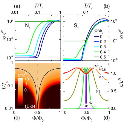
Figure 2(a) and (b) display the behavior of calculated for a few values of , for a normal () and a superconducting (S1) electrode, respectively. At low temperature () a large suppression of can be achieved for (i.e., down to ) due to the presence of a S-like DoS in the wire which leads to a reduction of quasiparticles available for thermal transport, and which is only limited by the finite value of . At fixed , then gradually increases, as displayed in Fig. 2(c) and (d), eventually coinciding with by closing the minigap at . We emphasize that although a heat valve effect could be achieved as well by replacing the N1 electrode with a superconductor S1 [see Fig 2(b)], the performance of the resulting structure, apart a stronger quenching of at low , worsen owing to the presence of the energy gap in S1 which severely limits the heat current flow. For this reason in the following we will focus on the properties of the nanovalve implemented with a N1 electrode. In order to obtain large modulations a tunnel contact between the N wire and N1 is crucial. The presence of a clean metallic contact indeed leads to a drastic degradation of the superconducting-like properties of the N-wire due to inverse proximity effect Bezuglyi and Vinokur (2003).
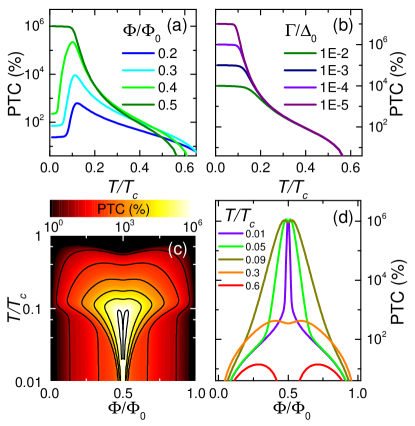
The heat valve efficiency of this setup can be quantified through the phase-dependent thermal conductance ratio (PTC) defined as: . As can be noticed in Fig. 3(a) and (c), where the PTC ratio is calculated vs and , respectively, the nanovalve can be highly efficient at temperatures below with a PTC exceeding 100% for , and saturating to at for , as shown in Fig. 3(b). Moreover, at low temperature, the thermal valve is more sensitive to the magnetic flux , as demonstrated by the sharp open/close transitions appearing around in Fig. 3(d).
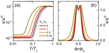
All the above results have been obtained from Eq. (2), which is valid in the limit of a short N-wire. In the case of an arbitrary length we have solved numerically the Usadel equation (1) in the N regionVirtanen and Heikkilä (2007); Virtanen (2009) to obtain the DoS in the middle of the wire and compute the thermal conductance from Eq. (3). The solutions are shown in Fig. 4 where the behavior of in and is displayed for different . At large the solutions converge to the analytical one (represented by the dashed lines) that well approximates for . Moreover, the general trend of in and is reproduced also for longer wires () with a damping of still three order of magnitude smaller than at low temperatures (i.e., for ), therefore ensuring full functionality of the thermal nanovalve even for .
According to the above conditions the experimental realization of our thermal nanovalve can be easily achieved with conventional metals and standard lithographic techniques Giazotto et al. (2010); Meschke et al. (2011); Jabdaraghi et al. (2014); Ronzani et al. (2014). Superconducting tunnel junctions additionally coupled to the SN ring and the N1 electrode, serving either as heaters or thermometers, allow to change and monitor the quasiparticle temperature on both sides of the structure Giazotto et al. (2006). We neglect here the contribution to thermal transport through these probes as they can provide nearly-ideal thermal isolation of the nanovalve electrodes.
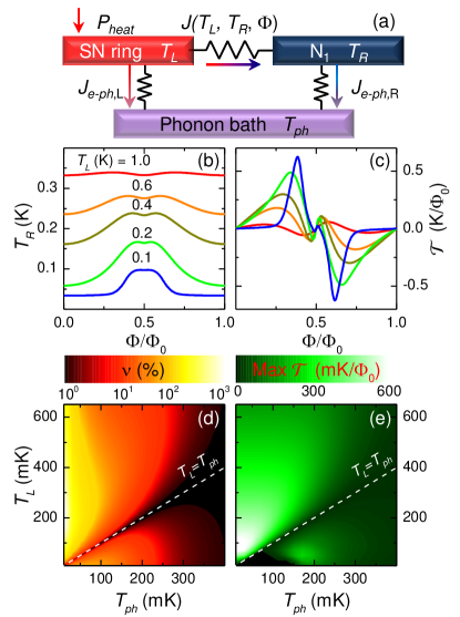
Figure 5(a) shows the relevant model accounting for thermal transport in the device. Upon intentionally heating the SN ring at the steady-state electron temperature will depend on the heat exchange mechanisms occurring in N1. Below K, the energy relaxation mechanism in N1 stems mainly from electron-acoustic phonon interaction Giazotto et al. (2006), , which allows heat exchange between quasiparticle and lattice phonons residing at . Above, is the material-dependent electron-phonon coupling constant, is the volume, and is the characteristic exponent of the N1 metal. In the model we neglect thermal transport mediated by photons Schmidt et al. (2004); Meschke et al. (2006); Pascal et al. (2011) as well as pure heat conduction by phonons Maki and Griffin (1965). For any given and , the steady-state is then obtained by solving the thermal balance equation . For the following calculations we assume an aluminum (Al) ring with eV, , , m3, and WK-6m-3 as appropriate for an AlMn N1 electrode Martínez-Pérez et al. (2014); Martínez-Pérez and Giazotto (2014). Furthermore, we assume the SNS junction to be in the short limit which, according to the above discussions, properly describes the framework of a realistic nanovalve Meschke et al. (2011); Jabdaraghi et al. (2014); Ronzani et al. (2014).
Phase-dependent control of thermal current through the nanovalve is demonstrated by the strong modulation of displayed in Fig. 5(b) for different values of at mK. In particular, it can exceed mK at mK. The high response of the heat valve, quantified by the flux-to-heat current transfer coefficient () Giazotto and Martínez-Pérez (2012b, a), is demonstrated in Fig. 5(c) where is plotted for the same values of panel (b). In particular, obtains values as large as mK at 20 mK and for , and it keeps increasing at lower , as shown in Fig. 5(e). Moreover, to quantify the visibility of temperature modulation induced by the magnetic flux we define the parameter , where . A full characterization of as a function of and is shown in Fig. 5(d). According to the calculations, a sizeable modulation is still visible () up to 300 mK of bath temperature and, differing from the SQUID-based thermal modulator Giazotto and Martínez-Pérez (2012b), the visibility is strongly enhanced at lower exceeding 1000% at 20 mK. Notably, the proximity nanovalve demonstrates good performance also for the temperature regime where , as shown by the high efficiency and large transfer functions visible in the regions below the white dashed lines of panels (d) and (e).
In summary, we have proposed a thermal nanovalve based on the SQUIPT technology which is able to efficiently conduct or isolate heat depending on the magnitude of an applied magnetic flux. Under experimentally accessible conditions the device can provide full phase control of the thermal conductance, which is unique at cryogenic temperatures. Standard nanolithographic techniques and conventional metals provide a straightforward route towards the implementation of this thermal nanovalve.
We acknowledge P. Virtanen for fruitful discussions. The work of E.S. and F.G. was partially funded by the European Research Council under the European Union’s Seventh Framework Programme (FP7/2007-2013)/ERC grant agreement No. 615187-COMANCHE, and by the Marie Curie Initial Training Action (ITN) Q-NET 264034. The work of F.S.B was supported by the Spanish Ministry of Economy and Competitiveness under Project No. FIS2011-28851-C02- 02 the Basque Government under UPV/EHU Project No. IT-756-13.
References
- Martínez-Pérez et al. (2014) M. J. Martínez-Pérez, P. Solinas, and F. Giazotto, J. Low Temp. Phys. 175, 813 (2014).
- Giazotto and Martínez-Pérez (2012a) F. Giazotto and M. J. Martínez-Pérez, Nature 492, 401 (2012a).
- Giazotto and Martínez-Pérez (2012b) F. Giazotto and M. J. Martínez-Pérez, Appl. Phys. Lett. 101, 102601 (2012b).
- Martínez-Pérez and Giazotto (2013) M. J. Martínez-Pérez and F. Giazotto, Appl. Phys. Lett. 102, 092602 (2013).
- Martínez-Pérez and Giazotto (2014) M. J. Martínez-Pérez and F. Giazotto, Nat. Commun. 5 (2014), 10.1038/ncomms4579.
- Eom et al. (1998) J. Eom, C.-J. Chien, and V. Chandrasekhar, Phys. Rev. Lett. 81, 437 (1998).
- Dikin et al. (2001) D. A. Dikin, S. Jung, and V. Chandrasekhar, Phys. Rev. B 65, 012511 (2001).
- Bezuglyi and Vinokur (2003) E. V. Bezuglyi and V. Vinokur, Phys. Rev. Lett. 91, 137002 (2003).
- Giazotto et al. (2010) F. Giazotto, J. T. Peltonen, M. Meschke, and J. P. Pekola, Nat. Phys. 6, 254 (2010).
- Meschke et al. (2011) M. Meschke, J. T. Peltonen, J. P. Pekola, and F. Giazotto, Phys. Rev. B 84, 214514 (2011).
- Jabdaraghi et al. (2014) R. N. Jabdaraghi, M. Meschke, and J. P. Pekola, Appl. Phys. Lett. 104, 082601 (2014).
- Ronzani et al. (2014) A. Ronzani, C. Altimiras, and F. Giazotto, arXiv:1404.4206 [cond-mat] (2014).
- Guéron et al. (1996) S. Guéron, H. Pothier, N. O. Birge, D. Esteve, and M. H. Devoret, Phys. Rev. Lett. 77, 3025 (1996).
- Zhou et al. (1998) F. Zhou, P. Charlat, B. Spivak, and B. Pannetier, J. Low Temp. Phys. 110, 841 (1998).
- Usadel (1970) K. D. Usadel, Phys. Rev. Lett. 25, 507 (1970).
- Dynes et al. (1984) R. C. Dynes, J. P. Garno, G. B. Hertel, and T. P. Orlando, Phys. Rev. Lett. 53, 2437 (1984).
- Pekola et al. (2004) J. P. Pekola, T. T. Heikkilä, A. M. Savin, J. T. Flyktman, F. Giazotto, and F. W. J. Hekking, Phys. Rev. Lett. 92, 056804 (2004).
- Pekola et al. (2010) J. P. Pekola, V. F. Maisi, S. Kafanov, N. Chekurov, A. Kemppinen, Y. A. Pashkin, O.-P. Saira, M. Möttönen, and J. S. Tsai, Phys. Rev. Lett. 105, 026803 (2010).
- Saira et al. (2012) O.-P. Saira, A. Kemppinen, V. F. Maisi, and J. P. Pekola, Phys. Rev. B 85, 012504 (2012).
- Kuprianov and Lukichev (1988) M. Y. Kuprianov and V. F. Lukichev, Sov. Phys. JETP 67, 1163 (1988).
- le Sueur et al. (2008) H. le Sueur, P. Joyez, H. Pothier, C. Urbina, and D. Esteve, Phys. Rev. Lett. 100, 197002 (2008).
- Hammer et al. (2007) J. C. Hammer, J. C. Cuevas, F. S. Bergeret, and W. Belzig, Phys. Rev. B 76, 064514 (2007).
- Giazotto and Bergeret (2013) F. Giazotto and F. S. Bergeret, Appl. Phys. Lett. 102, 162406 (2013).
- Levchenko (2008) A. Levchenko, Phys. Rev. B 77, 180503 (2008).
- Reutlinger et al. (2014) J. Reutlinger, L. Glazman, Y. V. Nazarov, and W. Belzig, Phys. Rev. Lett. 112, 067001 (2014).
- Courtois et al. (2008) H. Courtois, M. Meschke, J. T. Peltonen, and J. P. Pekola, Phys. Rev. Lett. 101, 067002 (2008).
- Giazotto et al. (2006) F. Giazotto, T. T. Heikkilä, A. Luukanen, A. M. Savin, and J. P. Pekola, Rev. Mod. Phys. 78, 217 (2006).
- Virtanen and Heikkilä (2007) P. Virtanen and T. T. Heikkilä, Appl. Phys. A 89, 625 (2007).
- Virtanen (2009) P. Virtanen, “Quasiclassical equations on a 1d network,” (2009), source code for the solution of the Usadel equation available at http://ltl.tkk.fi/~theory/usadel1/.
- Schmidt et al. (2004) D. R. Schmidt, R. J. Schoelkopf, and A. N. Cleland, Phys. Rev. Lett. 93, 045901 (2004).
- Meschke et al. (2006) M. Meschke, W. Guichard, and J. P. Pekola, Nature 444, 187 (2006).
- Pascal et al. (2011) L. M. A. Pascal, H. Courtois, and F. W. J. Hekking, Phys. Rev. B 83, 125113 (2011).
- Maki and Griffin (1965) K. Maki and A. Griffin, Phys. Rev. Lett. 15, 921 (1965).