Topological phase transition and quantum spin Hall state in TlBiS2
Abstract
We have investigated the bulk and surface electronic structures and band topology of TlBiS2 as a function of strain and electric field using ab-initio calculations. In its pristine form, TlBiS2 is a normal insulator, which does not support any non-trivial surface states. We show however that a compressive strain along the (111) direction induces a single band inversion with Z2 = (1;000), resulting in a Dirac cone surface state with a large in-plane spin polarization. Our analysis shows that a critical point lies between the normal and topological phases where the dispersion of the 3D bulk Dirac cone at the -point becomes nearly linear. The band gap in thin films of TlBiS2 can be tuned through an out-of-the-plane electric field to realize a topological phase transition from a trivial insulator to a quantum spin Hall state. An effective model Hamiltonian is presented to simulate our first-principles results on TlBiS2.
I Introduction
The interplay between spin-orbit coupling (SOC) and topological band theory gives rise to a new state of quantum matter known as a topological insulator (TI)hasan ; qi ; qshe in which band orderings become inverted in relation to their natural order at certain high symmetry points in the bulk Brillouin zone. TIs support spin-dependent conductive states at their boundaries while remaining insulating in the bulk, and are thus topologically distinct from the normal insulators. The topological surface states are protected by time reversal symmetry and exhibit nearly linear energy dispersion with unique spin-textures where spin is locked perpendicular to momentum. The topological protection guarantees backscattering-free transport at the boundaries of TIs. Due to the existence of these novel surface states, the TIs not only offer potential applications in quantum computing and spintronicsnayak_QC , but also pave the way for realizing novel quantum phenomena such as Weyl semimetalswan ; murakami ; singh1 , Majorana-fermionsmajorana and Higgs mechanismhiggs ; mass in a condensed matter system.
First principles calculations have led to the prediction of a large number of three-dimensional (3D) and two-dimensional (2D) TIs, which include 2D HgTe/CdTe quantum wellsbervenig ; konig , bismuth and antimony based V2VI3 binary thermoelectricszhang ; hsieh ; xia , and many ternary compounds ranging from the Tl-compounds to the half-Heusler family, among otherslin ; yan_tl ; neupane ; heuslar ; throughput ; apervoskite . TIs usually feature a band inversion, driven by the high SOC associated with the heavier atoms in the material, at the time reversal invariant momenta (TRIM) in the bulk Brillouin zone. Thus the tuning of SOC can provide a pathway for inducing topological phase transitions (TPT) from the normal to the topological insulator state. One approach is to undertake chemical tuning, which however often entails uncontrolled effects of chemical disorder. Another common approach is to attempt modifying the band topology by adjusting lattice constants or internal atomic positions in the unit celllin ; singh1 ; heuslar ; gst225_ahuja ; hgse_blah ; zhu_st ; Inse ; ab1 ; ab2 ; ab3 .
Many theoretical studies show that a 2D TI or a quantum spin Hall (QSH) insulator, along with TPTs therein, are possible by tuning the thickness of quantum wells or via reduced dimensionality of 3D TIs in the form of thin-films. lin ; wada ; liubi2te3 ; yzhangnat584 ; APL_Sb ; singh2 ; InAsGaSbtheory ; InAsGaSbexp . The band topology of the thin films can also be controlled through an external transverse electric fieldAPL_Sb ; PNAS_sb2te3 ; PRL_hgcdte ; APL_helical , which could be provided by the substrate and/or controlled via gating. Despite many theoretical proposals, the QSH state has been realized to date only in HgTe/CdTe and InAs/GaSb/AlSb quantum well systemsInAsGaSbexp ; konig . The need for finding new 2D materials, in which the QSH state TPTs can be realized, is thus clear.
In this paper, using systematic ab-inito calculations, we show that a 3D topological insulating phase as well a TPT can be induced in TlBiS2 through external strain, and that thin films of this material can realize the QSH phase and undergo a TPT as a function of external electric field. TlBiS2 is found to be a trivial insulator both theoretically and experimentally with a direct band gap at the point.lin ; higgs ; mass ; singh1 It exhibits a layered crystal structure with strong ionic and covalent type bonds within as well as between the layers. In sharp contrast, in the Bi2Se3 family of compounds,zhang ; zhu_st ; Inse blocks of layers are held together by weak van der Waals type bonding. The strong bonding between the layers in TlBiS2, on the other hand, makes this system a good prototype for the tuning and inversion of the band gap via the interlayer distance.
Bearing the preceding considerations in mind, we delineate in this study the evolution of topological band order in TlBiS2 with strain. Our analysis shows that a 3D-TPT occurs when a compressive strain is applied along the (111) direction, yielding an inverted band gap larger than 250 meV. The critical point between the normal and topological phase is accompanied by the formation of a single 3D bulk Dirac cone at the bulk Brillouin zone center with a nearly linear energy dispersion over a substantial energy range. Our slab computations further show that the (111) surface of strained TlBiS2 supports a single Dirac cone surface state at the -point. This surface state displays a large in-plane spin-polarization with small hexagonal warping effects. Moreover, we show that a 2D TPT as well as the QSH state can be realized in thin films of pristine TlBiS2 through an out-of-the-plane electric field. The critical point in this case supports six spin-polarized Dirac cones along the directions. Finally, we discuss a simple model Hamiltonian that captures the salient features of our first-principles bulk and surface states in TlBiS2.
The organization of the present article is as follows. In section II, we give the computational details and discuss the bulk crystal and band structures. Section III explains the evolution of topological band order in TlBiS2 under strain. Section IV considers the surface electronic structures at various strain values and the associated non-trivial spin-textures. The evolution of the QSH state through an out-of-the-plane electric field is discussed in Section V. In Sec. VI, we give the Hamiltonian for TlBiS2. In Sec. IV, we make brief concluding remarks.
II Computational methods and bulk band structures
We employed the density functional theory (DFT) frameworkkohan with projector augmented wave (PAW) methodpaw as implemented in the VASP packagevasp . The generalized-gradient approximation (GGA)pbe was used to model exchange-correlation effects. SOC was taken into account self-consistently to treat relativistic effects. The relaxed structural parameters from Ref. singh1, were used. The plane-wave cutoff energy of 350 eV was employed, and an -centered k-mesh was used for bulk computations. The strain was simulated by varying lattice constant ’’ of TlBiS2. For surface computations, we employed the slab model with periodically repeated slabs with a vacuum of 12 Å and a -centered 9 9 1 k-mesh. Surface relaxation is well-known to play an important role in slab computationslin ; singh1 , and therefore, all atomic positions were optimized until the residual force on each atom was less than 0.005 eV/Å. In order to resolve spin-textures of topological states, we carried out computations on a fine k-mesh in the vicinity of the Dirac point, and obtained the three spin components at each k-point from the expectation values of the three Pauli spin matrices , and .
TlBiS2 belongs to the Tl-family of compoundslin ; yan_tl ; singh1 . It has a rhombohedral crystal structure with four atoms in the primitive unit cell. The space group is (, SG no. 166). The conventional hexagonal unit cell has 12 atoms corresponding to three formula units in which the layers are stacked in the order Tl-S-Bi-S along the z-axis, see Figure 1(a). Each Tl(Bi) layer is sandwiched between the two S layers, so that the bonding between all the layers is strongsingh1 , and the material is essentially 3D, and it is quite distinct from the Bi2Se3 family where the quintuple layer blocks are bonded via weak van-der Waals forces. TlBiS2 possesses inversion symmetry like Bi2Se3, with Tl or Bi layers providing inversion centers. As a result, topological invariants for the band structure can be computed straightforwardly from the parities of the Bloch wave functions at the TRIM pointskane .
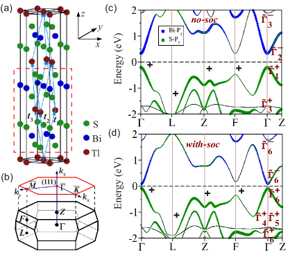
The bulk band structures without and with SOC are shown in Figs. 1(c) and (d). Without the SOC, TlBiS2 is a direct gap semiconductor with a band gap of 0.64 eV at . The band decomposed charge densities and symmetries show that the bulk valence band (BVB) is composed of S states and belongs to representation of space group zhang_model ; yan_tl ; footnote_parity . In contrast, the bulk conduction band (BCB) is composed of Bi states and belongs to representation. A parity analysiskane reveals that TlBiS2 has Z2 = (0;000). When we include the SOC, a large shift in the energies of all the bands occurs throughout the bulk Brillouin zone (BZ), and the band gap shrinks significantly to a value of 0.26 eV [Fig. 1(d)], but all bands remain two-fold spin degenerate. Within a spinor representationzhang_model , the BVB and BCB belong to and representations of the double group of , respectively, as shown in Fig. 1(d). Although the SOC modifies the electronic structure significantly, it induces no band inversions, and the material remains a trivial insulator.
III 3D Topological phase transition
III.1 Bulk analysis
We have shown previously that the electronic structure of TlBi(S1-xSex)2 alloys singh1 can be tuned from a normal to a non-trivial insulating phase by modulating the coupling potential. The inversion symmetry is explicitly broken in this case, yielding a semimetal phase at the critical point singh1 . Here, we consider the ordered, inversion symmetric TlBiS2 system and use a compressive strain to modify its electronic structure. Note in this connection that crystal field splitting (CFS) in TlBiS2 lifts the degeneracy between the pz and px/py orbitalsyan_tl ; zhang . Any changes in the BiS and TlS bonds now lead to associated changes in the CFS, and hence in the band gap. Accordingly, we consider a uniaxial compressive strain along the trigonal axis and monitor the band gap for a possible band inversion. Relaxation of in-plane lattice constants ’’ and ’’ was found to have a negligible effect over the band gap at when interlayer distance ’’ was reduced. For this reason, we fixed the in-plane lattice constants to their bulk relaxed values and varied only ’’. The strain is defined as where , is the difference between the strained and relaxed lattice constant.
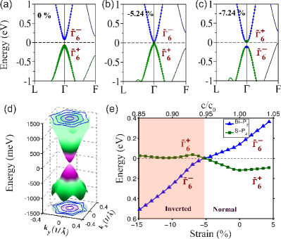
The strain dependent band structure in Figs. 2(a)(c) shows that as we increase the compressive strain along the (111) direction, the band gap starts decreasing as the BVB and BCB levels start approaching each other, and closes at the critical strain value of -5.24%, see Fig. 2(b). Based on the dependence of free energy on the lattice parametersmurnaghan , we estimate that a pressure of 3.13.5 GPa would be sufficient to induce such a strain. The band gap is seen from Fig. 2(c) to become inverted with a further increase in strain. An analysis of the band structure of Fig. 2(c) indicates that the band gap extends over the entire BZ. Evolution of and levels over a wide range of strains is shown in Fig. 2(e). The inverted band gap is seen to attain a value of 0.28 eV at -10.24% strain, which is fairly large compared to other Tl compounds. It could be increased further with increased strain, although such large strains would be difficult to realize in practice. We have verified the topological nature of band structure of TlBiS2 at various strain values via parity analysis. Illustrative results at two different strain values, one at which the system is trivial and another at which it is non-trivial, are presented in Table I. These results show that the topological phase is induced via a single band inversion at the -point with increasing strain.
| Strain | 1 | L 3 | F 3 | Z 1 | Z2 |
|---|---|---|---|---|---|
| 0 % | (0;000) | ||||
| -7.24 % | (1;000) |
Fig. 2(d) shows a 3D rendition of the Dirac cone states at the critical strain value of Fig. 2(b). Interestingly, the constant energy contours (CECs) are seen to be nearly circular in shape up to about 800 meV with linear dispersion, and would allow access to Dirac physics over a fairly high energy range.
III.2 Surface electronic structure and spin-texture
Figs. 3(a)(c) consider the surface electronic structure based on fully relaxed slabs of TlBiS2 at three different values of strain. As expected, at 0% strain (Fig. 3(a)), only a trivial band gap is seen without the presence of gapless surface states. With increasing strain, the gap between the bulk bands (shaded cyan region) closes at the critical strain value in Fig. 3(b), and reopens with the appearance of Dirac cone states lying within the bulk band gap (Fig. 3(c)). The surface states in Fig. 3(c) cross the Fermi energy an odd number of times between the and -points, demonstrating that strained TlBiS2 is a strong topological insulator.
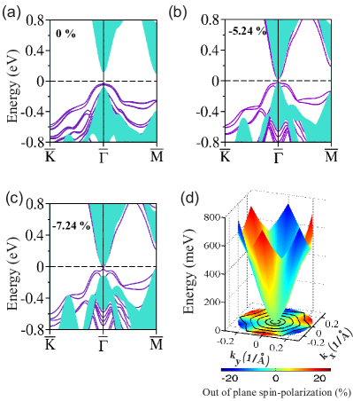
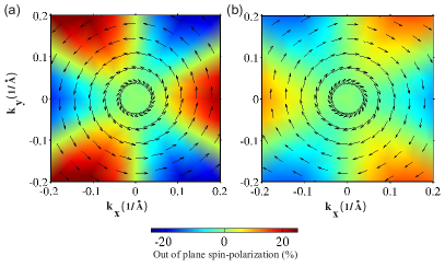
Figure 3(d) shows the nearly linear 3D energy dispersion of the upper portion of the topological surface state in the plane with small hexagonal warpingHexawarp ; susmita . The CECs are essentially circular up to an energy of 500 meV. Spin textures of the upper and lower surface Dirac cones are further examined in Fig. 4. Spin is seen to be locked perpendicular to momentum over a large portion of the k-space with both the upper and lower cones displaying distinct chiralities. As one moves away from the Dirac point, the spin-texture acquires a finite out-of-the-plane spin component as the Dirac cone becomes hexagonally warped.
IV 2D Topological phase transition and Quantum spin Hall state
2D TPTs as well as the QSH state can be realized in thin films of 3D topological insulators through effects of reduced dimensionality liubi2te3 ; yzhangnat584 ; APL_Sb ; singh2 ; wada . In particular, when the film thickness becomes smaller than the surface state decay length, quantum tunneling between the top and bottom surfaces of the film opens a thickness dependent gap at the Dirac point. The surface state decay length in Tl compounds is ,lin ; singh1 and therefore, films with less than about 30 atomic layers would be suitable for realizing the QSH state. Strained films of TlBiS2, which we have shown above to assume the 3D topological insulator phase, would thus be appropriate candidates for realizing a 2D TPT and the QSH statesingh2 .
We will however explore an alternate route for achieving the QSH state in films of TlBiS2 in the normal insulator phase by subjecting these films to an external electric field (gating). APL_Sb ; PNAS_sb2te3 ; PRL_hgcdte ; APL_helical Application of an out-of-the-plane electric field () breaks the inversion symmetry of the film as two sides of the film become inequivalent. As a result, the spin degeneracy of states away from the TRIM points is lifted. In this way, the electric field provides a mechanism for realizing spin-polarized states and gating controlled TPTs in thin films. Note that topological invariants now cannot be obtained through a parity analysis, but adiabatic continuity arguments must be deployed. We have specifically done so here by monitoring the band gap while varying strength of the SOC from 0-100%.
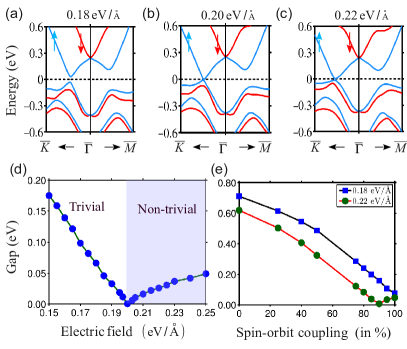
The slab configuration with seven layers in which the S atom is in the top layer followed by Bi [See Fig. 1(a)] exhibits a minimum number of dangling bond states.lin ; singh1 The band structure of such a relaxed 7L slab of TlBiS2 is considered in Figs. 5(ac) near the -point under an external electric field, . In the absence of an electric field, the 7L thin film is an indirect band gap semiconductor with a band gap of 0.45 eV, and all states are at least twofold spin degenerate due to inversion symmetry. As we apply the electric field, the spin degeneracy away from the TRIM points is lifted and the band gap begins to decrease. By monitoring the band gap size as a function of applied electric field, as shown in Figure 5(d), the gap closes at the critical field value of 0.20 eV/Å along the direction, see Figs. 5(b) and (d). At this critical point, the valence and conduction bands touch each other at six points, and form six spin-polarized Dirac cones along the directions. With further increase in the electric field the gap reopens (inverted) again the system assumes a QSH state; the topological nature of this state can be established by monitoring the band gap as a function of SOC strength as shown in Fig. 5(e). For eV/Å, the gap decreases from 0.7 eV at 0% to 0.08 eV at 100 % SOC strength without closing at any intermediate value of the SOC. Therefore, the band structures with and without the SOC are connected adiabatically and hence are both topologically trivial. On the other hand, for eV/Å, the gap closes at 90 % SOC strength and reopens with a value of 0.05 eV at 100 %, allowing us to conclude that the 7L film is in the QSH state for fields greater than 0.20 eV/Å. Along the preceding lines, we also investigated thicker slabs of 11L, 15L and 19L using atomic configuration similar to that of the 7L slab; all these slabs were found to exhibit the QSH state for relatively small values of the external electric field. We also examined thinner 5L slabs with Bi or Tl atoms in the top layer. These slabs also transition into the QSH state with critical field value of 0.10-0.15 eV/Å, although the critical topological point now lies within the dangling bond states. The preceding results show clearly that pristine TlBiS2 films can be switched between the normal and QSH states under the action of a perpendicular external electric field.
V model Hamiltonian
We now discuss a model Hamiltonian which captures the interesting physics of TlBiS2. Since the bulk band structure undergoes band inversion at only the -point, it is appropriate to consider an effective Hamiltonian near the -point, which takes into account symmetry properties of the systemWinkler_kp . For this purpose, we need to identify the irreducible representations of the symmetry group for both the valence and the conduction bands at the -point. In the trivial phase, the BVB is mainly composed of S anti-bonding states, whereas the BCB is composed of Bi bonding states. For convenience, we denote the BVB as and BCB as , where indicates the parity of the corresponding states. The four states involved thus are: (,,, ). The crystal structure of TlBiS2 (rhombohedral with space group ) is the same as that of Bi2Se3 and TlBiTe2. The wavefunctions at can therefore be classified along the lines of Bi2Se3 and TlBiTe2zhang ; zhang_model ; yan_tl , see Ref. zhang_model, for details. As discussed in section II above, the BVB and BCB belong to and representations, respectively. Keeping all this in mind, the four band effective Hamiltonian of Bi2Se3 is applicable here, which in the basis (,,, )zhang ; zhang_model ; yan_tl , is:
| (1) |
| (2) |
| (3) |
with , , , and . Here, preserves the in-plane rotation symmetry, whereas reduces it to a threefold rotation symmetry. The parameters , , , , , , , , , and are calculated numerically by fitting to ab-inito dispersions, and are given for 0% (trivial region) and -7.24 % (non-trivial region) strain in Table 2. At -7.24 % strain, , , and , which implies that the system stays in the inverted region and thus remains topologically non-trivial for larger strains.
| Parameter | 0% | -7.24% |
|---|---|---|
| (eV Å) | 1.04 | 1.83 |
| (eV Å) | 3.06 | 2.72 |
| (eV) | -0.0035 | -0.0011 |
| (eV Å2) | 1.97 | 4.3 |
| (eV Å2) | 3.616 | 2.337 |
| (eV ) | -0.0859 | 0.0714 |
| (eV Å2) | 2.14 | 0.368 |
| (eV Å2) | 21.08 | 18.67 |
| (eV Å3) | 22.81 | 16.12 |
| (eV Å3) | 48.23 | 38.23 |
The non-trivial surface dispersion for TlBiS2 can be directly computed from the above model Hamiltonian using appropriate boundary conditionskonig ; zhang_model ; yan_tl . Here, we consider the semi-infinite system for which the Hamiltonian of Eq. (1) applies only for . It can then be shown straightforwardly that the two localized states and , which are Kramer’s partners, appear at the surface only if , i.e. in the inverted regime. The effective Hamiltonian for the surface can be extracted by projecting the bulk Hamiltonian (1) on to the space spanned by these two states as:
| (4) |
Here, the parameters , , , and depend upon the material and the boundary conditions. The term is coupled to and breaks the in-plane rotation symmetry to a three fold rotation symmetry. This is the counterpart of cubic Dresselhaus spin-orbit coupling in the bulk rhombohedral structures and ensures the appearance of an out-of-the-plane spin-component, and explains the hexagonal warping observed in Figure 5 Hexawarp . The term, and hence the component, vanishes along the mirror directions.
The surface band dispersion of using , and the bulk values of the parameters in equation (4), is:
| (5) |
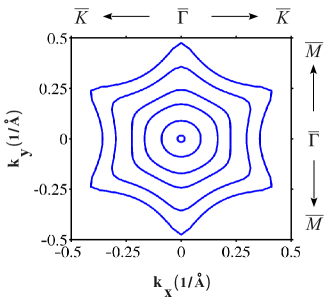
where denotes the energy of upper (conduction) and lower (valence) bands. Figure 6 shows the CECs for upper (conduction) band calculated using this dispersion. The CECs are circular near the Dirac point, but as we move away from the Dirac point, the CECs become hexagonal due to -term Hexawarp . The hexagonal warping is maximum along the directions, whereas it vanishes along the mirror directions. As we further increase the energy away from the Dirac point, the CECs attain a snowflakes shape where vertices lie along the directions. These features of CECs are in good agreement with our ab-initio results.
VI Conclusion
We discuss how strain and electric field could be used to tune the bulk and surface electronic structures of TlBiS2 using ab-intio DFT calculations. In its relaxed, pristine structure TlBiS2 is found to be a normal insulator without any surface states. However, the system undergoes a 3D topological phase transition under 5.24 % compressive strain with the formation of 3D bulk Dirac cone states with nearly linear energy dispersion. The inverted band gap attains a value of 0.28 eV for 10.24% compressive strain, and the band gap could be increased further by increasing strain. Through slab computations, we show that Dirac cone surface state has a nearly linear energy dispersion with a large in-plane spin-polarization. We show that the a 2D topological phase transition from a normal insulator to the QSH state can be realized in thin films of TlBiS2 by varying the strength of an electric field perpendicular to the film surface. Finally, we present a model Hamiltonian for bulk and surface states of strained TlBiS2. Our results indicate that TlBiS2 films are a viable candidate for realizing a gating controlled on/off switch between the normal and QSH states.
Acknowledgments
This work was supported by the Department of Science and Technology, New Delhi (India) through project SR/S2/CMP-0098/2010. H.L. acknowledge the Singapore National Research Foundation for support under NRF Award No. NRF-NRFF2013-03. The work at Northeastern University is supported by the US Department of Energy, Office of Science, Basic Energy Sciences contract DE-FG02-07ER46352, and benefited from theory support at the Advanced Light Source and the allocation of supercomputer time at NERSC through DOE grant number DE-AC02-05CH11231.
References
- (1) M. Z. Hasan and C. L. Kane, Rev. Mod. Phys. 82, 3045 (2010).
- (2) X.-L. Qi and S.-C. Zhang, Rev. Mod. Phys. 83, 1057 (2011).
- (3) B. A. Bernevig and S.-C. Zhang, Phys. Rev. Lett. 96, 106802 (2006).
- (4) C. Nayak, S. H. Simon, A. Stern, M. Freedman, and S. Das Sarma, Rev. Mod. Phys. 80, 1083 (2008).
- (5) X. Wan, A. M. Turner, A. Vishwanath, and S. Y. Savrasov, Phys. Rev. B 83, 205101 (2011).
- (6) S. Murakami, New Journal of Physics 9, 356 (2007).
- (7) B. Singh, A. Sharma, H. Lin, M. Z. Hasan, R. Prasad, and A. Bansil, Phys. Rev. B 86, 115208 (2012).
- (8) F. Wilczek, Nat. Phys. 5, 614 (2009).
- (9) T. Sato, K. Segawa, K. Kosaka, S. Souma, K. Nakayama, K. Eto, T. Minami, Y. Ando, and T. Takahashi, Nat. Phys. 7, 840 (2011).
- (10) S.-Y. Xu, Y. Xia, L. A. Wray, S. Jia, F. Meier, J. H. Dil, J. Osterwalder, B. Slomski, A. Bansil, H. Lin, R. J. Cava, and M. Z. Hasan, Science 332, 560 (2011).
- (11) B. A. Bernevig, T. L. Hughes, and S.-C. Zhang, Science 314, 1757 (2006).
- (12) M. Konig, S. Wiedmann, C. Brüne, A. Roth, H. Buhmann, L. W. Molenkamp, X.-L. Qi, and S.-C. Zhang, Science 318, 766 (2007).
- (13) H. Zhang, C.-X. Liu, X.-L. Qi, X. Dai, Z. Fang, and S.-C. Zhang, Nat. Phys. 5, 438 (2009).
- (14) D. Hsieh, D. Qian, L. Wray, Y. Xia, Y. S. Hor, R. J. Cava, and M. Z. Hasan, Nature 452, 970 (2008).
- (15) Y. Xia, D. Qian, D. Hsieh, L. Wray, A. Pal, H. Lin, A. Bansil, D. Grauer, Y. S. Hor, R. J. Cava, and M. Z. Hasan, Nat. Phys. 5, 398 (2009).
- (16) H. Lin, R. S. Markiewicz, L. A. Wray, L. Fu, M. Z. Hasan, and A. Bansil, Phys. Rev. Lett. 105, 036404 (2010).
- (17) B. Yan, C.-X. Liu, H.-J. Zhang, C.-Y. Yam, X.-L. Qi, T. Frauenheim, and S.-C. Zhang, EPL (Europhysics Letters) 90, 37002 (2010).
- (18) M. Neupane et al., Phys. Rev. B 85, 235406 (2012).
- (19) H. Lin, L. A. Wray, Y. Xia, S. Xu, S. Jia, R. J. Cava, A. Bansil, and M. Z. Hasan, Nat. Mater. 9, 546 (2010).
- (20) K. Yang, W. Setyawan, S. Wang, M. Buongiorno Nardelli, and S. Curtarolo, Nat Mater 11, 614 (2012).
- (21) Y. Sun, X.-Q. Chen, S. Yunoki, D. Li, and Y. Li, Phys. Rev. Lett. 105, 216406 (2010).
- (22) B. Sa, J. Zhou, Z. Sun, and R. Ahuja, EPL (Europhysics Letters) 97, 27003 (2012).
- (23) L. Winterfeld, L. A. Agapito, J. Li, N. Kioussis, P. Blaha, and Y. P. Chen, Phys. Rev. B 87, 075143 (2013).
- (24) Z. Zhu, Y. Cheng, and U. Schwingenschlögl, Phys. Rev. Lett. 108, 266805 (2012).
- (25) Y. Ma, Y. Dai, L. Yu, C. Niu, and B. Huang, New Journal of Physics 15, 073008 (2013).
- (26) It will be interesting to consider combined effects of strain and disorder on the surface and bulk electronic structures using various approaches; see, for example, Refs. ab2, ; ab3, .
- (27) A. Bansil, Phys. Rev. Lett. 41, 1670(1978); R. Prasad and A. Bansil, Phys. Rev. B21, 496(1980); L. Schwartz and A. Bansil, Phys. Rev. B 10, 3261 (1974).
- (28) H. Lin, S. Sahrakorpi, R.S. Markiwicz, and A. Bansil, Phys. Rev. Lett. 96, 097001 (2006); S.N. Khanna, A.K. Ibrahim, S.W. McKnight, and A. Bansil, Solid State Commun. 55, 223 (1985); L. Huisman, D. Nicholson, L. Schwartz and A. Bansil, Phys. Rev. B24, 1824 (1981).
- (29) M. Wada, S. Murakami, F. Freimuth, and G. Bihlmayer, Phys. Rev. B 83, 121310 (2011).
- (30) C.-X. Liu, H. Zhang, B. Yan, X.-L. Qi, T. Frauenheim, X. Dai, Z. Fang, and S.-C. Zhang, Phys. Rev. B 81, 041307 (2010).
- (31) Y. Zhang et al., Nat Phys 6, 584 (2010).
- (32) F.-C. Chuang, C.-H. Hsu, C.-Y. Chen, Z.-Q. Huang, V. Ozolins, H. Lin, and A. Bansil, Applied Physics Letters 102, 022424 (2013).
- (33) B. Singh, H. Lin, R. Prasad, and A. Bansil, Phys. Rev. B 88, 195147 (2013).
- (34) C. Liu, T. L. Hughes, X.-L. Qi, K. Wang, and S.-C. Zhang, Phys. Rev. Lett. 100, 236601 (2008).
- (35) I. Knez, R.-R. Du, and G. Sullivan, Phys. Rev. Lett. 107, 136603 (2011).
- (36) M. Kim, C. H. Kim, H.-S. Kim, and J. Ihm, Proceedings of the National Academy of Sciences 109, 671 (2012).
- (37) W. Yang, K. Chang, and S.-C. Zhang, Phys. Rev. Lett. 100, 056602 (2008).
- (38) G. Liu, G. Zhou, and Y.-H. Chen, Applied Physics Letters 99, 222111 (2011).
- (39) P. Hohenberg and W. Kohn, Phys. Rev. 136, B864 (1964).
- (40) G. Kresse and D. Joubert, Phys. Rev. B 59, 1758 (1999).
- (41) G. Kresse and J. Furthmüller, Phys. Rev. B 54, 11169 (1996).
- (42) J. P. Perdew, K. Burke, and M. Ernzerhof, Phys. Rev. Lett. 77, 3865 (1996).
- (43) L. Fu and C. L. Kane, Phys. Rev. B 76, 045302 (2007).
- (44) represents the product of parity eigenvalues of the occupied bulk bands at the TRIM points and is given as where N is the number of occupied bulk bands and is the parity eigenvalue of the 2mth occupied energy band at the point .
- (45) C.-X. Liu, X.-L. Qi, H. Zhang, X. Dai, Z. Fang, and S.-C. Zhang, Phys. Rev. B 82, 045122 (2010).
- (46) The superscript represents the parity eigenvalue associated with the irreducible representations.
- (47) F. D. Murnaghan, Proc. Natl Acad. Sci. USA 30, 244 (1944).
- (48) L. Fu, Phys. Rev. Lett. 103, 266801 (2009).
- (49) S. Basak, H. Lin, L. A. Wray, S.-Y. Xu, L. Fu, M. Z. Hasan, and A. Bansil, Phys. Rev. B 84, 121401 (2011).
- (50) R. Winkler, Spin–Orbit Coupling Effects in Two-Dimensional Electron and Hole Systems (Springer Tracts in Modern Physics, Springer, 2003), Vol. 191.