Proximity induced topological state in graphene
Abstract
The appearance of topologically protected states at the surface of an ordinary insulator is a rare occurrence and to date only a handful of materials are known for having this property. An intriguing question concerns the possibility of forming topologically protected interfaces between different materials. Here we propose that a topological phase can be transferred to graphene by proximity with the three-dimensional topological insulator Bi2Se3. By using density functional and transport theory we prove that, at the verge of the chemical bond formation, a hybrid state forms at the graphene/Bi2Se3 interface. The state has Dirac-cone-like dispersion at the point and a well-defined helical spin-texture, indicating its topologically protected nature. This demonstrates that proximity can transfer the topological phase from Bi2Se3 to graphene.
pacs:
61.46.Km,73.63-b,62.25.-gTopological insulators (TIs) are a recently discovered class of materials presenting an electronic band-gap in the bulk and metallic edge states at their surfaces 1, 2, 3. The peculiarity is that the edge states are protected against electron scattering to impurities, so that they can act as perfectly ballistic conductors 1, 4. To date only a handful of TIs have been synthesized and high-throughput materials screening has indicated that only few more may be fabricated by straining existing inorganic compounds 5. Intriguingly, with the only exception of CdTe/HgTe-quantum wells 6, there are no reports of two-dimensional (2D) TIs. Thus at the moment we have at hand only three-dimensional (3D) TIs with 2D edge states. Yet, one may wonder whether we have exhausted all the possibilities for creating useful topologically protected states in materials.
A particularly intriguing prospect is that of using the interaction between different materials to create hybrid interfaces with topological properties. For instance depositing normal semiconductors on top of 3D topological insulators may result in a structure that under certain conditions exhibits topologically protected interface states 7. An even more attractive prospect is that of using that protocol for transferring topologically protected states to graphene 8, 9. Since graphene-based transistors have been already demonstrated 10, one could then speculate on having graphene logic elements connected by topological-graphene interconnects, i.e. on realizing an all graphene high-performance logic circuitry. A major advantage of such strategy is its fully compatible with 2D patterning.
Several proposals have been already brought forward for making graphene topological 11. Indeed one of the first TIs models was based on a staggered hexagonal lattice with helicity-dependent complex hopping parameter, simulating spin-orbit interaction 12. However, since spin-orbit coupling in graphene is tiny, a topological phase may be induced only by strongly perturbing the graphene electrostatic potential, for instance by adsorbing heavy ions on top of the sheet 13. Importantly, although theoretically sound, such proposal requires ultra-accurate fabrication precision and appears rather challenging in practice. Here we suggest a completely different approach: we introduce topologically protected states in graphene by proximity with a lattice-commensurate 3D TI. This happens at the graphene/Bi2Se3 interface, a composite which was synthesized about two years ago 14, 15, 16, but whose electronic structure still remains unclear.
I Computational methods
Calculations are performed by density functional theory (DFT) as implemented in the VASP code 17, 18. We use the Perdew-Burke-Ernzerhof form of the generalized gradient approximation 19 and the core electrons are described by projector-augmented-wave pseudopotentials 20. The -space integration spans a Monkhorst-Pack mesh in the irreducible Brillouin zone and the plane waves cutoff is 400 eV.
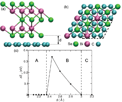
The geometry of the structure investigated is shown in Fig. 1. We consider a Bi2Se3 slab containing three quintuple layers (QLs), for which the tensile stress is minimal among the experimentally investigated Bi2Se3/graphene composites 14. The Bi2Se3 unit cell is commensurate with three graphene unit cells, hence the elementary unit cell of the composite contains an entire carbon ring. The contacting Se atom is placed at the graphene hollow site (in the center of the ring). The in-plane lattice parameter is 4.26 Å, which is only 2.3% larger than the lattice parameter of bulk Bi2Se3 21; the one perpendicular to the interface is instead 40 Å (there is a vacuum region 10 Å between cells periodic replica). We have also investigated a second geometry where the carbon atoms are on top of Se. This, however, is not energetically favorable and it has not been considered in the rest of the paper. Interestingly both interface structures present rather similar trends in the electronic structure properties.
II Results and discussion
Let us begin by investigating the evolution of the graphene band-gap with the graphene/Bi2Se3 distance, . We assign an electronic band to a given material by projecting the energy and -dependent wave function onto spherical harmonics centered around particular atoms 22. We define the graphene electronic band-gap from those bands located near the charge neutral point of free-standing graphene and having dominant C character. In Fig. 1(c) one can identify three different regions. For Å [region C] graphene has no band-gap. This is expected since for large separations the interaction is weak and the band-structure of the composite is the superposition of those of the constituents. As such graphene remains a zero-gap semiconductor. Region B is characterized by the opening of the graphene band-gap. The gap increases monotonically from Å and it reaches a maximum (0.34 eV) for Å. A further reduction in (region A) closes the gap, which remains close up to Å.
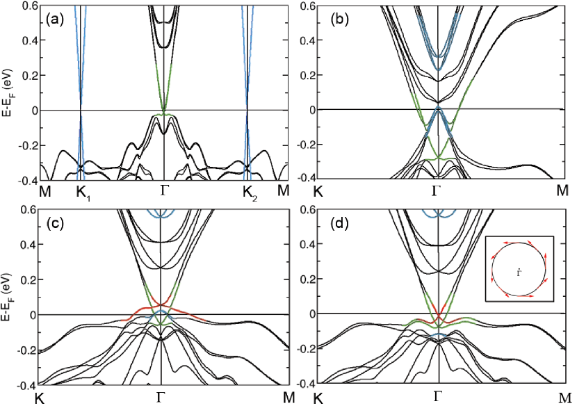
Next we analyze in Fig. 2 the nature of the graphene bands around the Fermi level, , as a function of . For Å [Fig. 2(a)] the composite features two superimposed band-structures corresponding to those of graphene and Bi2Se3, respectively. At such large separation there is no wave function overlap between graphene and Bi2Se3, leaving the two materials electronically decoupled. The graphene’s linearly dispersive bands (in blue in Fig. 2) at each of the valleys (Dirac K-points) are 2-fold spin-degenerate, with the () and () bands just touch each other. The Bi2Se3 surface states (green bands in Fig. 2) cross at the point.
Decreasing below 3 Å causes a band-gap opening between the and bands [see Fig. 2(b), Å]. Now the graphene valleys are placed together with the Bi2Se3 surface states around the point due to the bands folding in the supercell structure. As the graphene electronic gap increases further upon a reduction of [see Å, Fig. 2(c)], the cone lifts up in energy but the tip of the one remains pinned at . The topologically protected surface states of Bi2Se3 (one per surface) are positioned in the vicinity of the tip of the cone. For separations Å these surface states form a doubly-degenerate state since the two surfaces are equivalent for the unperturbed TI slab. For distances Å the symmetry of the TI slab breaks due to the vicinity of the graphene layer and the degeneracy of the surface states is lifted. The TI surface state in contact with graphene moves up in energy at by about 0.11 eV for Å. Importantly, the graphene states that are pinned at start to couple with the surface state and, for Å, the 4-fold degeneracy of the cone is lifted. Here the pure graphene bands forming the cone are pushed down in energy and only the mixed graphene/Bi2Se3 band [red in Fig. 2(d)] and the Bi2Se3 surface state at the opposite side of the interface (placed directly beneath the mixed band at ) cross .
Intriguingly, such newly formed mixed graphene/Bi2Se3 band presents a helical spin-texture, demonstrated in the inset of Fig. 2(d). This is a sufficient condition for disabling back-scattering of charge carriers 1, and it is not the case in a pristine graphene sheet. In fact, defects in graphene allow hopping of charge carriers between two valleys, which causes back-scattering due to their opposite winding numbers. In contrast, hopping is impossible in systems with only one valley and a helical spin-texture, which is the case for graphene/Bi2Se3. Note, however, that the existence of the helical spin texture and the lack of back-scattering do not necessarily mean topological protection of the material’s electronic state 23.
The supercell structure causes the folding of the second Brillouin zone (BZ) of primitive graphene into the first and consequently the migration of the graphene valleys from K to . Thus two 4-fold degenerate cones touching at are formed. The bands from the two valleys have opposite topological charges, which causes their mutual annihilation 24. This manifests itself in the opening in graphene of a band-gap [see Fig. 2(b) and (c)], much larger than that estimated for thallium adatoms deposition 13.
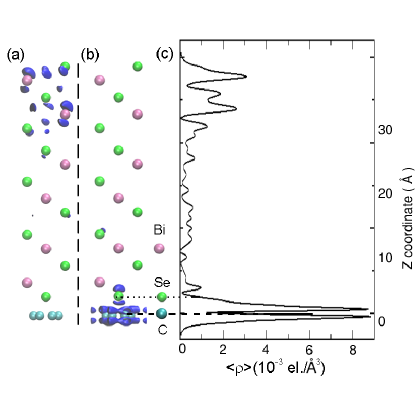
After having determined the emergence of a mixed graphene/Bi2Se3 band, we now analyze in detail its electronic properties. The electron density integrated over a narrow energy region around and projected over the mixed state is shown in Fig. 3(b). This is clearly localized over graphene and, to a smaller degree, over the Se atoms in contact to graphene. Since such state presents a dominating C- and Se- orbital contribution and it is delocalized in the plane of the interface, it presents conjugation. A more quantitative insight is obtained by plotting the charge density averaged over planes parallel to the interface [Fig. 3(c)]. This shows that, while the contribution to the electron density originating from the bulk is small, a much larger portion is provided by the two surface states at both sides of the composite. At the free Bi2Se3 surface the surface state is distributed mainly over the first four atomic layers [Fig. 3(a)]. In contrast, at the graphene/Bi2Se3 interface the electron density migrates from the TI to graphene. Notably this feature resembles closely the one reported for the interface between the normal metal Sb2Se3 and the TI Bi2Se3 25. Also the behavior is similar to the topologization of ZnM (M=S, Se, Te) upon deposition on Bi2Se3 7.
Let us now spend a few words on the possibility of inducing a topological state in graphene due to its proximity and bonding to Bi2Se3. Firstly, we wish to point out that our results do not indicate that graphene converts into a 2D topological insulator upon its deposition on Bi2Se3, but simply that a topologically-protected hybrid state is formed. A 2D TI is an insulator in the bulk presenting topologically protected 1D states at the edges of a ribbon, as in the case of Bi thin films on Bi2Te3 surface 26, 27. In contrast here the Fermi surface of graphene undergoes a transition from a zero-band gap semiconducting phase (region C), prone to gap opening due to defects and impurities, to a topologically protected metallic phase (region A) via an insulating phase (region B). A fundamental property of 3D TIs is the existence of an odd number of surface bands around . Another property is that the topology of the surface states is such to connect the bulk valence band to the conduction one due to the parity inversion originated by the strong spin-orbit coupling. In the graphene/Bi2Se3 complex only one conical band is present at the Fermi level. Importantly this band belongs to the surface state of Bi2Se3 with considerable contribution of graphene around , while the other parts of the state (in particular the ends that connect to the valance and the conduction bulk TI states) still fully belong to the TI. Thus the topologically protected surface TI state can be understood as a carrier of the induced graphene states, and the intrinsic topological protection of TI surface state provides the robustness to graphene as well.
The topologically-protected hybrid state does not simply correspond to the penetration of the one of the Bi2Se3 edge states into graphene. In that situation interaction between Bi2Se3 and graphene is not present. In contrast here the interaction is strong and, in fact, as decreases first it is responsible for the opening of a band-gap in graphene and then for creating the topologically-protected hybrid state. This behaviour is very similar to that of the Sb2Se3/Bi2Se3 25 and the ZnM/Bi2Se3 (M=S, Se, Te) 7 interfaces, in which a topological state is transferred to the normal metal because of proximity.
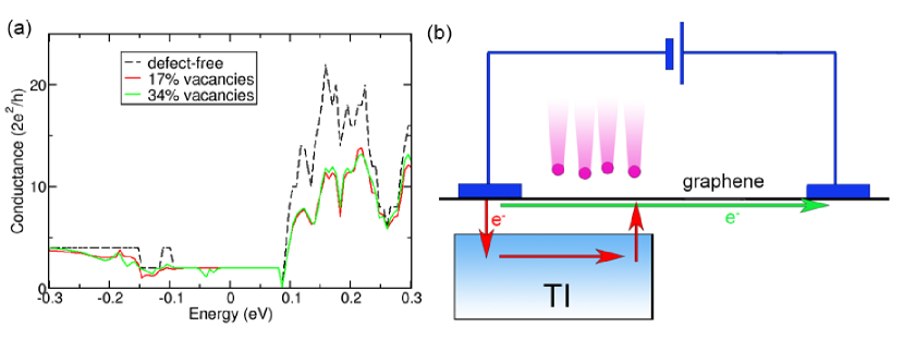
As a final characterization of the hybrid state we have probed its scattering properties. In particular we have performed transport calculations, with the Smeagol code 28, for the composite along the direction parallel to the graphene sheet. Note that Smeagol provides an electronic structure for the composite essentially identical to that obtained with VASP. We have then calculated the system conductance for a defect-free system and for a the case where approximately 17% or 33% vacancies counting atoms are introduced along the direction perpendicular to the transport [see Fig. 4(a)]. Note that these are extremely large concentrations and here they serve the purpose to prove the topological protection of the surface state. From Fig. 4(a) one can observe that 17% of vacancies do not affect the conductance around indicating that the state is indeed strongly protected against back-scattering. Even for a 33% concentration little reduction of the conductance is found at around , although the graphene layer is almost cut in two parts. Note, however, that the inclusion of impurities reduces significantly the conductance for energies away from the Fermi level, i.e. away the topologically protected part of the graphene spectrum. This demonstrate that the transport is indeed through graphene and it is protected against back-scattering at around the Fermi level.
In concluding we would like to propose an experiment, which may prove the transfer of the topologically protected state to graphene. A schematic view of the proposed setup is shown in Fig. 4(b), in which a graphene sheet is contacted only in part to Bi2Se3 while the rest remains free-standing. Defects are then introduced in graphene only at the contacting region for instance by electrons or ions irradiation 29. If there exists topological protection in graphene at the contact region, the electronic transport through such system will not show a conductance reduction relative to that of the defect-free case. One may still argue that the transport through the irradiated region is via the topologically protected surface state of Bi2Se3 rather than through the defective graphene. However, in this case the charge carriers need to hop between the TI and the contacting graphene [red arrows in Fig. 4(b)] in order to continue their flow through the bare graphene and close the electric circuit. This will degrade the conductance. In contrast if the transport is carried solely by states of the (defected) graphene the effects of hopping will be eliminated by the proposed geometry setup.
Throughout the paper we have presented results as a function of the graphene/Bi2Se3 distance, therefore we would like to close this section by briefly discussing what equilibrium distance one can expect. Unfortunately this turns out to be a difficult problem. The exact binding distance is determined by a balance between covalent and van der Waals forces. These latter ones are not captured by DFT local/semi-local exchange and correlation functionals and in fact we find that the two materials do not bind when the calculation is done at the generalized gradient approximation level 19. This contrasts reality where the graphene/Bi2Se3 exists as it has been experimentally fabricated by few groups 14, 15, 16. Unfortunately the inclusion of van der Waals forces at the level of local DFT 30 does not improve the situation, as screening prevents an accurate evaluation of the binding energy in layered compounds 31. However we expect the equilibrium graphene/Bi2Se3 distance to be close to the sum of Se and C covalent radii, which amounts to 2Å. This is well within region A [see Fig.1(c)], i.e. when the hybrid surface state forms. Besides, external pressure may be introduced for tuning the desired separation.
III Conclusions
In conclusion, we have investigated the electronic properties of graphene in contact to Bi2Se3. Three phases have been identified,
depending on the graphene/Bi2Se3 separation. For Å, the electronic structure of the composite is simply the superposition
of those of the constituents. The second phase, obtained for 2.4 Å 3.0 Å, witnesses the opening of a band-gap in graphene,
due to the annihilation of graphene states with opposite winding numbers. The third phase, when graphene and Bi2Se3 chemically bind,
is the most interesting, as a topologically protected state with charge distribution mostly localized on graphene forms.
Acknowledgments
This work is sponsored by Science Foundation of Ireland (SFI) under the CSET grant underpinning CRANN and under the QDFUN project
(Grant No. 07/IN.1/I945). AN acknowledges financial support from the Irish Research Council.
Computational resources have been provided by the HEA IITAC project managed by TCHPC.
Note added: While our manuscript was under review, we became aware of a related work investigating Bi2Se3/graphene/Bi2Se3 quantum wells 32. Although the details of such work are different we find an agreement for the range of lattice spacing where the two sets of calculations can be compared.
References
- Hasan and Kane 2010 M. Hasan and C. Kane, Rev. Mod. Phys. 82, 3045 (2010).
- Manoharan 2010 H. Manoharan, Nat. Nano. 5, 477 (2010).
- Zhang et al. 2009 H. Zhang, C.-H. Liu, X.-L. Qi, X. Dai, Z. Fang, and S.-C. Zhang, Nat. Phys. 5, 438 (2009).
- Park et al. 2010 K. Park, J. J. Heremans, V. W. Scarola, and D. Minic, Phys. Rev. Lett. 105, 186801 (2010).
- Yang et al. 2012a K. Yang, W. Setyawan, S. Wang, M. B. Nardelli, and S. Curtarolo, Nature Materials 11, 614 (2012a).
- König et al. 2007 M. König, S. Wiedmann, C. Brüne, A. Roth, H. Buhmann, L. W. Molenkamp, X.-L. Qi, and S.-C. Zhang, Science 318, 766 (2007).
- Wu et al. 2013 G. Wu, H. Chen, Y. Sun, X. Li, P. Cui, C. Franchini, J. Wang, X.-Q. Chen, and Z. Zhang, Sci. Rep. 3, 1233 (2013).
- Wei and Liu 2010 D. Wei and Y. Liu, Adv. Mater. 22, 3225 (2010).
- Geim and Novoselov 2007 A. Geim and K. Novoselov, Nat. Mater. 6, 183 (2007).
- Lin et al. 2011 Y.-M. Lin, A. Valdes-Garcia, S.-J. Han, D. B. Farmer, I. Meric, Y. Sun, Y. Wu, C. Dimitrakopoulos, A. Grill, P. Avouris, et al., Science 332, 1294 (2011).
- Li et al. 2011 J. Li, M. Büttiker, and A. Morpurgo, Physica Scripta T146, 1 (2011).
- Kane and Mele 2005 C. L. Kane and E. J. Mele, Phys. Rev. Lett. 95, 226801 (2005).
- Weeks et al. 2011 C. Weeks, J. Hu, J. Alicea, M. Franz, and R. Wu, Phys. Rev. X 1, 021001 (2011).
- Dang et al. 2010 W. Dang, H. Peng, H. Li, P. Wang, and Z. Liu, Nano Lett. 10, 2870 (2010).
- Song et al. 2010 C.-L. Song, Y.-L. Wang, Y.-P. Jiang, Y. Zhang, C.-Z. Chang, L. Wang, K. he, X. Chen, J.-F. Jia, Y. Wang, et al., Appl. Phys. Lett. 97, 143118 (2010).
- Jiang et al. 2012 Y. Jiang, Y. Sun, M. Chen, Y. Wang, Z. Li, C. Song, K. He, L. Wang, X. Chen, Q.-K. Xue, et al., Phys. Rev. Lett. 108, 066809 (2012).
- Kresse and Furthmüller 1996a G. Kresse and J. Furthmüller, Phys. Rev. B 54, 11169 (1996a).
- Kresse and Furthmüller 1996b G. Kresse and J. Furthmüller, Comput. Mater. Sci. 6, 15 (1996b).
- Perdew et al. 1996 J. P. Perdew, K. Burke, and M. Ernzerhof, Phys. Rev. Lett. 77, 3865 (1996).
- Blöchl 1994 P. E. Blöchl, Phys. Rev. B 50, 17953 (1994).
- Lind and Lidin 2003 H. Lind and S. Lidin, Solid State Sc. 5, 47 (2003).
- Furthmüller et al. 1996 J. Furthmüller, J. Hafner, and G. Kresse, Phys. Rev. B 53, 7334 (1996).
- Tse and MacDonald 2010 W.-K. Tse and A. MacDonald, Phys. Rev. B 82, 161104(R) (2010).
- Vozmediano et al. 2010 M. Vozmediano, M. Katsnelson, and F. Guinea, Phys. Rep. 496, 109 (2010).
- Zhang et al. 2012 Q. Zhang, Z. Zhang, Z. Zhu, U. Schwingenschlögl, and Y. Cui, ACS Nano 6, 2345 (2012).
- Hirahara et al. 2012 T. Hirahara, N. Fukui, T. Shirasawa, M. Yamada, M. Aitani, H. Miyazaki, M. Matsunami, S. Kimura, T. Takahashi, S. Hasegawa, et al., Phys. Rev. Lett. 109, 227401 (2012).
- Yang et al. 2012b F. Yang, L. Miao, Z. Wang, M.-Y. Yao, F. Zhu, Y. Song, M.-X. Wang, J. Xu, A. Fedorov, Z. Sun, et al., Phys. Rev. Lett. 109, 016801 (2012b).
- Rocha et al. 2006 A. Rocha, V. Garcia-Suarez, S. Bailey, C. Lambert, J. Ferrer, and S. Sanvito, Phys. Rev. B 73, 085414 (2006).
- Robertson et al. 2012 A. W. Robertson, C. Allen, Y. Wu, K. He, J. Olivier, J. Neethling, A. Kirkland, and J. Warner, Nature Comm. 3, 1144 (2012).
- Dion et al. 2004 M. Dion, H. Rydberg, E. Schroder, D. C. Langreth, and B. I. Lundqvist, Phys. Rev. Lett. 92, 246401 (2004).
- Cunningham et al. 2012 G. Cunningham, M. Lotya, C. Cucinotta, S. Sanvito, S. Bergin, R. Menzel, M. Shaffer, and J. N. Coleman, ACS Nano 6, 3468 (2012).
- Kou et al. 2013 L. Kou, B. Yan, F. Hu, S. Wu, T. Wehling, C. Felser, C. Chen, and T. Frauenheim, arXiv 1310.2580 (2013).