Electronic excitations and structure of Li2IrO3 thin films grown on ZrO2:Y (001) substrates
Abstract
Thin films are a prerequisite for application of the emergent exotic ground states in iridates that result from the interplay of strong spin-orbit coupling and electronic correlations. We report on pulsed laser deposition of Li2IrO3 films on ZrO2:Y(001) single crystalline substrates. X-ray diffraction confirms preferential (001) and (10-1) out-of-plane crystalline orientations with well defined in-plane orientation. Resistivity between 35 and 300 K is dominated by a three-dimensional variable range hopping mechanism. The dielectric function is determined by means of spectroscopic ellipsometry and, complemented by Fourier transform infrared transmission spectroscopy, reveals a small optical gap of 300 meV, a splitting of the - manifold, and several in-gap excitations attributed to phonons and possibly magnons.
pacs:
68.55.-a, 71.27.+a, 75.50.LkI Introduction
The layered perovskite oxides A2IrO3 (A = Na, Li) have in recent years been studied in terms of a physical realization of the Kitaev and Heisenberg-Kitaev model and its extensions, harboring spin liquid and topologically ordered phases. Kitaev (2006); Jackeli and Khaliullin (2009); Chaloupka, Jackeli, and Khaliullin (2010); Reuther, Thomale, and Trebst (2011); Singh et al. (2012); Reuther, Thomale, and Rachel (2014) They have also drawn interest as possible topological insulators. Shitade et al. (2009); Pesin and Balents (2010); Kim et al. (2012a, 2013) Ultimately, the physical realization of such states of matter is desired with respect to quantum computation proposals. Kitaev (2003); Collins (2006); Nayak et al. (2008) Subsequently, experiments showed that both materials order magnetically at 15 K: Na2IrO3 is deep within an antiferromagnetically zig-zag ordered phase, Singh and Gegenwart (2010); Ye et al. (2012); Liu et al. (2011); Choi et al. (2012) whereas Li2IrO3 shows incommensurate spiral order but is placed close to the desired spin liquid phase. Kobayashi et al. (2003); Singh et al. (2012); Reuther, Thomale, and Rachel (2014) There is yet no direct experimental evidence of a topological insulator phase in either of the two materials.
Some of us have previously reported on the first successful growth of heteroepitaxial Na2IrO3 thin films, where we observed three-dimensional variable range hopping conductivity and the weak antilocalization effect in magnetoresistance. Jenderka et al. (2013) To date, available single crystals are of very small size, such that experimental data on Li2IrO3 is often restricted to powder-averaged data. Kobayashi et al. (1997, 2003); Singh et al. (2012); Gretarsson et al. (2013) Certain types of experiments, such as terahertz pump-probe spectroscopy or neutron diffraction, benefit from large-area single-crystalline thin film samples. Neutron diffraction experiments, for instance, are challenging because of a high absorption cross-section of iridium and the small crystal sizes. Thin films however alleviate these problems by distributing the volume over a large area. If its growth was feasible, thin films would in general also allow for the study of strain-induced effects. In fact, both a strain-induced spin liquid and topological insulator phase are proposed to exist. Reuther, Thomale, and Trebst (2011); Singh et al. (2012); Kim et al. (2012a, 2013) Hence, thin films of this class of material lay a foundation for future experiments including e.g. studies on the (Na1-xLix)2IrO3 compounds, which are not available in single crystalline form so far.
Like its sister compound Na2IrO3, Li2IrO3 is an antiferromagnetic insulator with Neél temperature 15 K below which it orders in an incommensurate spiral fashion. Kobayashi et al. (2003); Singh et al. (2012); Reuther, Thomale, and Rachel (2014) X-ray powder diffraction measurements suggest a monoclinic C2/c unit cell. Kobayashi et al. (2003); Singh et al. (2012) Temperature dependent resistivity shows insulating behavior between 100 and 300 K. Singh et al. (2012) A delicate interplay between trigonal distortions of the IrO6 octaeder and spin-orbit coupling cause the spin-orbit assisted Mott insulating state. Until recently, the magnitude of the trigonal distortions was unclear. Consequently, the adequate description of the underlying electronic structure was under debate. Mazin et al. (2012, 2013); Bhattacharjee, Lee, and Kim (2012) However, recent resonant inelastic x-ray scattering experiments Gretarsson et al. (2013) validate the applicability of the so-called physics in Li2IrO3, which in the past was applied to Sr2IrO4 and related materials Kim et al. (2008); Moon et al. (2008); Kuriyama et al. (2010); Lee et al. (2013): The cubic crystal field caused by the edge-sharing IrO6 octaeder splits the Ir 5 orbitals into a doublet and a triplet. The splitting between and is about 3 eV. Moon et al. (2006) Structural distortions of the monoclinic unit cell and the oxygen tetraeder, respectively create a trigonal crystal field. If this field is sufficiently small compared to spin-orbit coupling, the triplet further splits into a fourfold degenerate = 3/2 and a twofold degenerate = 1/2 band.
In this paper, we report on the pulsed laser-deposition of Li2IrO3 thin films and the study of their structure. Temperature-dependent resistivity is measured between 300 and 25 K. Employing spectroscopic ellipsometry, we determine the dielectric function in order to study and interpret low energy electronic excitations on the basis of physics. These results are complemented with optical transmission data measured with a Fourier transform infrared spectrometer.
II Experimental details
Li2IrO3 thin films were grown by pulsed laser depositon (PLD) on 10 10 mm2 ZrO2:Y(001) single crystals (YSZ). PLD was done with a 248 nm KrF excimer laser at a laser fluence of 2 Jcm-2. The phase-pure polycrystalline target was prepared by a solid state synthesis of Li2CO3 and IrO2 powders in a stochiometric ratio of 1.1:1. The mixture was homogenized, pressed and calcined in air for 24 h at 750∘C. Afterwards it was again ground, pressed and sintered for 72 h in 900∘C. Unfortunately, the target was rather soft. To improve it, attempts were made to employ high pressure sintering (HPS). However, the reducing conditions due to the graphite heater used in HPS, had a detrimental effect on the target composition.
The deposition procedure involved a nucleation layer grown with 300 laser pulses at 1 Hz, followed by another 30,000 pulses at 15 Hz. After deposition, the samples were annealed in situ at an oxygen partial pressure = 800 mbar. Film thickness was estimated at 400 nm by spectroscopic ellipsometry. The growth process was optimized with respect to high film crystallinity, i.e. high x-ray diffraction peak intensity. We have grown films at growth temperatures and oxygen partial pressures within the ranges from 550∘C to 700∘C, and from 0.1 mbar to 3.0 10-4 mbar, respectively. We note, that for larger deposition temperatures Li2IrO3 films decomposed as indicated by additional x-ray reflexes belonging to other phases, most likely IrxOy species. For these films, an energy dispersive x-ray (EDX) analysis gave a reduced Ir:O ratio of 1:2.13. Optimized films were grown at 600∘C and 3.0 10-4 mbar.
Investigations of the epitaxial relationship were performed with both a Panalytical X’Pert PRO Materials Research Diffractometer with parabolic mirror and PIXcel3D detector and a Philips X’Pert x-ray diffractometer equipped with a Bragg-Brentano powder goniometer using divergent/focusing slit optics and Cu Kα radiation. Surface morphology was investigated via a Park System XE-150 atomic force microscope in dynamic non-contact mode and a CamScan CS44 scanning electron microscope. Temperature dependent dc electrical resistivity was measured in van-der-Pauw geometry with dc magnetron-sputtered ohmic gold contacts. The dielectric function (DF) was determined via standard variable angle spectroscopic ellipsometry in the spectral range from 0.03 to 3.34 eV (IRSE). Infrared optical transmission in the spectral range from 0.14 to 1.30 eV was measured using a BRUKER IFS 66v/S Fourier transform infrared spectrometer in transmission mode (T-FTIR).
III Results & discussion
III.1 Crystal structure
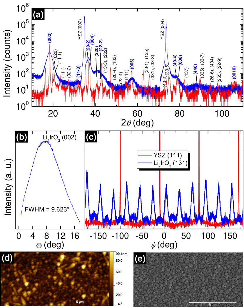
A typical x-ray diffraction (XRD) 2- pattern of a Li2IrO3 film is shown in Fig. 1(a). For confirmation of the preferential film orientations, the XRD pattern of the polycrystalline PLD target is underlayed. The patterns are indexed on the basis of a monoclinic unit cell Kobayashi et al. (2003); Singh et al. (2012). The pattern shows pronounced symmetric peaks related to the (001) and (10-1) planes of the Li2IrO3 phase, see blue labels in Fig. 1(a). The intensity ratio / is about 2.3:1 and thus much smaller than in the polycrystalline target ( 14:1). This strongly suggests preferential (001) and (10-1) out-of-plane crystalline orientations. However, peak assignment can be ambiguous, since in the monoclinic unit cell of Li2IrO3 many reflexes such as (20-2) & (004) are narrowly spaced. We fit the peak at = 36.88∘ with two Gaussians to obtain and . From the values of the (002), (004) and (006) reflexes, the lattice parameter is determined as 9.71(1) . We also performed - scans of the asymmetric (202) and (131) reflexes of the (001)-oriented phase and calculated lattice parameters = 5.20(3) and = 8.99(14) . For the calculations we assumed = 99.992∘. Kobayashi et al. (2003) The lattice parameters are in good agreement with reported values Kobayashi et al. (2003); Singh et al. (2012), , and deviating by +0.6%, +0.7% and -0.8% respectively. This indicates some amount of internal rather than epitaxial strain considering the significant lattice mismatch to YSZ(001).
A rocking curve of the (002) reflex at = 18.29∘ gives a full width at half maximum of about 10∘ (cf. Fig 1(b)).
Investigation of the in-plane epitaxial relationship is done by x-ray diffraction -scans of the asymmetric Li2IrO3 (131) reflex of the (001)-oriented phase and of YSZ (111), shown in Fig. 1(c). For YSZ(001), we observe the C4-symmetry of its (111) planes as expected. The -scan of the Li2IrO3 (131) reflection shows 12 + 12 reflections spaced by 15∘ alternating between ”high” and ”low” intensity peaks. Their intensity ratio is approximately 7:1. In Li2IrO3, the asymmetric (131) plane of both the (001)- and (10-1)-oriented phases share very similar angles. We therefore believe, that the -scan shows the rotational domains of both phases. Thus, it indicates that the C1-symmetric (monoclinic) (001)- and (10-1) oriented Li2IrO3 epilayers align in-plane within 12 rotational domains each. From the mismatch of rotational symmetry of substrate and epilayer, Grundmann, Böntgen, and Lorenz (2010) we expect a minimum of four rotational domains. The origin of the increased number of rotational domains is at present unknown. One explanation might however be possible: Initially, Li2IrO3 was reported as pseudo-hexagonal. Kobayashi et al. (1997) If it occurred, the existence of epitaxially induced C6-symmetry would lead, according to Ref. Grundmann, Böntgen, and Lorenz, 2010, to two rotational domains and thus 12 reflections in total per phase. Based on our x-ray data, it is not possible to determine the actual crystal structure of the epilayer, as the (001) planes of both monoclinic and pseudohexagonal symmetries share similar angles. Epitaxially induced change of lattice symmetry was e.g. observed for the growth of U3O8 on c-plane Al2O3. Burrell et al. (2007)
III.2 Chemical analysis and surface morphology
A qualitative elemental investigation of a film using secondary neutral mass spectrometry (SNMS) showed only Li, Ir, and O. An accumulation of volatile Li at the film-substrate interface was observed by SNMS depth profiling. However, it is currently not clear if the Ar+-sputtering in SNMS contributes to this Li accumulation at the interface. Energy dispersive x-ray analysis gave an oxygen deficient Ir:O ratio of 1:2.84 under the optimized PLD conditions, as discussed above. This ratio points to possible oxygen vacancies, that might in turn explain the internal strain observed in XRD.
Figures 1(d,e) show topographic images of the Li2IrO3 film surface obtained with non-contact atomic force microscopy (AFM) and scanning electron microscopy (SEM), respectively. The images reveal a granular surface with an RMS roughness of 15.7 nm and a peak-to-valley height of 139.0 nm. The surface morphology can be explained by the presence of two preferential orientations and furthermore by the mechanically soft target promoting grain agglomeration. We have in fact tried growing films on lattice-matched YAlO3(011) single crystals but observed no improvement in either crystalline structure or surface morphology.
III.3 Electrical resistivity
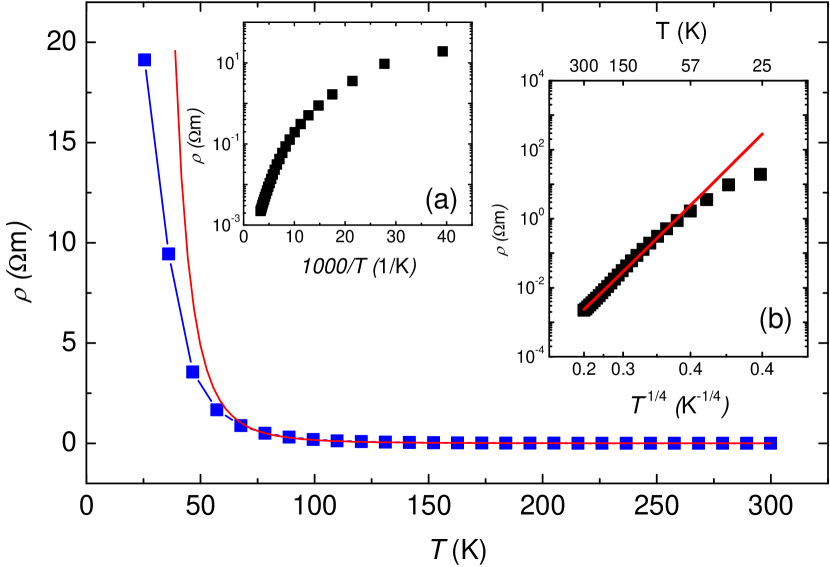
As illustrated in Fig. 2, Li2IrO3 exhibits semiconducting resistivity behavior between 300 and 25 K. Resistivity does not follow a simple activated law , see Fig. 2, inset (a), that can also be associated with nearest-neighbor hopping. Instead, resitivity follows a dependence down to at least 60 K. We associate this behavior to three-dimensional Mott variable range hopping (VRH), as similarly observed in Na2IrO3 thin films. Jenderka et al. (2013) Variable range hopping conduction results from localized states within a narrow energy band near the Fermi energy. At lower temperatures, resistivity diverges from this VRH dependence. As indicated by a straight line fit in Fig. 2, inset (b), we fit the resistivity data from 300 to 57 K with the three-dimensional Mott VRH model Mott (1969)
| (1) |
where is a temperature-dependent resisitivty coefficient and is the localization temperature. From the analysis of variable range hopping within percolation theory, the resisitivty coefficient is given by Shklovskii and Efros (1984); Arginskaya and Kozub (1994)
| (2) |
where 1/4. Fitting eq. (1) to the resistivity data, we extract = 2.0(4) 10-8 and a localization temperature of = 1.26(6) 107 K. An estimate for the localization length can be obtained from according to Shklovskii and Efros (1984)
| (3) |
provided that , the density of states at the Fermi level, is known. Based on available heat capacity data of Li2IrO3 and Na2IrO3 single crystals Singh et al. (2012), we assume 1028 eV-1m-3 (for details, see Ref. Jenderka et al., 2013). The calculated localization length is about 1.25(2) Å. Its magnitude is comparable with the Ir-Ir and Ir-O bond distances (approx. 3 and 2 Å, resp.) in the structurally very similar sister compound Na2IrO3, Choi et al. (2012); Ye et al. (2012) supporting the applicability of Mott VRH. A criterion for the validity of Mott VRH is that the average hopping distance be larger than the localization length , Mott (1968) i.e.
| (4) |
The ratio / is equal to 5.37(7) at 300 K satisfying above criterion. We also verify that the maximal hopping distance is much larger than the film thickness to exclude Mott VRH with hopping exponent 1/3. This kind of hopping is expected for thin films with thickness in the order of the maximal hopping distance Shante (1973)
| (5) |
Using the estimated localization length we obtain a maximal hopping distance of = 1.36(4) nm at 57 K which is much smaller than the film thickness 400 nm.
III.4 Spectroscopic ellipsometry
Spectra of the DF were determined from the ellipsometry data by using a model containing a layer for the substrate, a layer for the Li2IrO3 film and a surface roughness layer. Each layer is described by its thickness and optical constants. Between the substrate and the Li2IrO3 thin film, a thin interface layer of about 1 nm was introduced by mixing 50:50 the substrate and film DF in a ratio of 1:1 by means of a Bruggeman effective-medium approximation (EMA). Jellison et al. (1994) Also the surface roughness layer and the columnar structure was accounted for by a 100 nm EMA-layer by mixing the film DF with void. The void fraction was gradually increased from to 80% from bottom to top (please cf. note 111Please note that such a high surface roughness cannot be exactly described by this approach and the DF of the surface layer with their chosen gradient strongly correlates with the DF of the thin film. Therefore, for absolute values of the thin film DF a uncertainty of in the worst case has to be taken into account. But nevertheless, their general lineshape and the energy values of the electronic excitations and phonon modes are influenced far less and are therefore reliable. For the same reason we do not report because here the error amounts up to 50%.). For modelling the thin film’s DF we used a parametric model dielectric function (MDF) approach consisting of (cf. Fig. 3): a Drude free charge carrier absorption and two Lorentzians describing the phonon contribution at lowest energies; a near band gap Tauc-Lorentz (TcLo) absorption function Jellison and Modine (1996) and a series of M0-critical point functions with parabolic onset Adachi (1987); Yoshikawa and Adachi (1997) describing direct band-band transitions; Gaussian oscillators were used to model electronic band-band transitions spread within the Brillouin zone at higher energies. Additional discrete transitions where described by Lorentzians. Regression analysis was then applied to best match the dielectric function model to the experimental data. From the MDF, the absorption coefficient was calculated (cf. Fig. 4).
The final MDF together with its individual components is displayed in Fig. 3. In the following, we argue that these individual components represent electronic excitations that can be ascribed to transitions from and within the manifold in line with the picture of physics, as explained earlier in the text. We also show, that their transitions energies agree well with other experiments, such as angle-resolved photoemission spectroscopy (ARPES), resonant inelastic x-ray scattering (RIXS) and optical spectroscopy, performed on Li2IrO3, Na2IrO3 and other iridates. The observed excitations are summarized in Table 1.
In the high-energy spectral range above 1.2 eV, we find two contributions to the MDF at 1.63 and 3.25 eV that are attributed to - band transitions from occupied to empty bands (, ). Very similar transitions have been observed in Na2IrO3 and Li2IrO3 single crystals Comin et al. (2012); Gretarsson et al. (2013) and Na2IrO3 thin films. Jenderka et al. (2013) Below 1.2 eV, we find several transitions. The transitions at 55 and 65 meV are attributed to phonons; at 0.11 and 0.18 eV we find discrete transitions (). For example, in Sr2IrO4 a magnon was found at 0.2 eV within the Mott gap. Kim et al. (2012b) Further band-band excitations, possibly related to the particle-hole continuum boundary, Gretarsson et al. (2013) are found at 0.15 and more pronounced at 0.30 eV (). They imply a very narrow Mott gap of less than 0.3 eV. Narrow Mott gaps from 300 meV to 340 meV were also previously found in Na2IrO3 and Li2IrO3. Comin et al. (2012); Gretarsson et al. (2013); Jenderka et al. (2013) Another discrete transition can be recognized at 0.72 eV (). It is assigned to intraband transitions from = 3/2 to = 1/2 states. Excitations similar to were found in other iridates, as well. Moon et al. (2008); Kim et al. (2012b); Gretarsson et al. (2013)
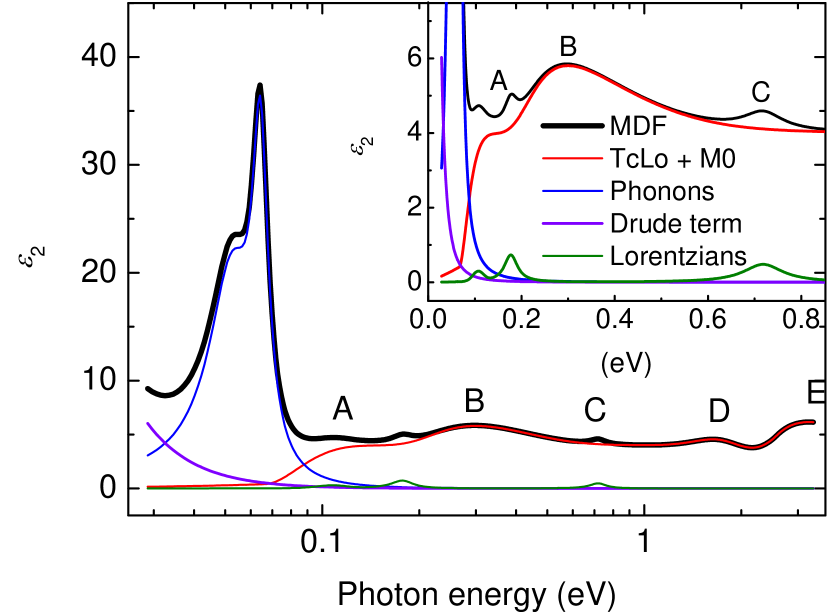
| Peak | A | B | B’ | C | C’ | D | E |
|---|---|---|---|---|---|---|---|
| Energy (eV) | 0.11, 0.18 | 0.3 | 0.43 | 0.72 | 0.89 | 1.63 | 3.25 |
| type of | magnon | = 3/2 | = 3/2 | = 3/2 | = 3/2 | ||
| excitation | (discrete) | = 1/2 | = 1/2 | = 1/2 | = 1/2 | (band-band) | (band-band) |
| (discrete) | (band-band) | (discrete) | (discrete) |
III.5 Infrared transmission spectroscopy
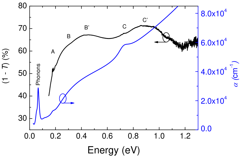
A transmission spectrum of the film was calculated from that of the entire sample and the substrate , measured each by means of T-FTIR, via .222The reflectivity of the thin film and the substrate is almost constant in that range and small, thus neglecting both introduces an error of less than 5% in . The (1-) spectrum (Fig. 4) also reveal a narrow optical gap below 0.3 eV . Furthermore two broad peaks with shoulders can be discerned indicating electronic excitations. To compare with the IRSE data, the absorption coefficient , calculated from the MDF, is included in Fig. 4 (blue curve) and the peak positions from Tab. 1 are indicated. Transitions - are reproduced in the T-FTIR data but are, however, complemented by transitions and (see Tab. 1).
IV Summary
In summary, we have grown Li2IrO3 thin films by means of PLD on YSZ(001) substrates. XRD confirms, that the films exhibit preferential (001) and (10-1) out-of-plane crystalline orientations with well defined in-plane orientation. Resistivity is dominated by three-dimensional variable range hopping. Electronic excitations below 3.34 eV were investigated via spectrocopic ellipsometry and transmission FTIR spectroscopy. On the basis of the physics and by comparison with related iridates, these excitations were associated to - transitions, transitions across the Mott gap and in-gap states. The optical gap was found to be , smaller than that of Na2IrO3 films.
Acknowledgements.
We thank the Deutsche Forschungsgemeinschaft (DFG) for financial support within the project LO790/5-1 ”Oxide topological insulator thin films”. We are grateful to Yvonne Joseph and Uwe Sczech of Institut für Elektronik- und Sensormaterialien, TU Freiberg for high pressure sintering of PLD targets.References
- Kitaev (2006) A. Kitaev, Annals of Physics 321, 2 (2006).
- Jackeli and Khaliullin (2009) G. Jackeli and G. Khaliullin, Physical Review Letters 102, 017205 (2009).
- Chaloupka, Jackeli, and Khaliullin (2010) J. Chaloupka, G. Jackeli, and G. Khaliullin, Physical Review Letters 105, 027204 (2010).
- Reuther, Thomale, and Trebst (2011) J. Reuther, R. Thomale, and S. Trebst, Physical Review B 84, 100406 (2011).
- Singh et al. (2012) Y. Singh, S. Manni, J. Reuther, T. Berlijn, R. Thomale, W. Ku, S. Trebst, and P. Gegenwart, Physical Review Letters 108, 127203 (2012).
- Reuther, Thomale, and Rachel (2014) J. Reuther, R. Thomale, and S. Rachel, Physical Review B 90, 100405 (2014).
- Shitade et al. (2009) A. Shitade, H. Katsura, J. Kuneš, X.-L. Qi, S.-C. Zhang, and N. Nagaosa, Physical Review Letters 102, 256403 (2009).
- Pesin and Balents (2010) D. Pesin and L. Balents, Nature Physics 6, 376 (2010).
- Kim et al. (2012a) C. H. Kim, H. S. Kim, H. Jeong, H. Jin, and J. Yu, Physical Review Letters 108, 106401 (2012a).
- Kim et al. (2013) H.-S. Kim, C. H. Kim, H. Jeong, H. Jin, and J. Yu, Physical Review B 87, 165117 (2013).
- Kitaev (2003) A. Kitaev, Annals of Physics 303, 2 (2003).
- Collins (2006) G. P. Collins, Scientific American 294, 56 (2006).
- Nayak et al. (2008) C. Nayak, A. Stern, M. Freedman, and S. Das Sarma, Reviews of Modern Physics 80, 1083 (2008).
- Singh and Gegenwart (2010) Y. Singh and P. Gegenwart, Physical Review B 82, 064412 (2010).
- Ye et al. (2012) F. Ye, S. Chi, H. Cao, B. C. Chakoumakos, J. A. Fernandez-Baca, R. Custelcean, T. F. Qi, O. B. Korneta, and G. Cao, Physical Review B 85, 180403 (2012).
- Liu et al. (2011) X. Liu, T. Berlijn, W.-G. Yin, W. Ku, A. Tsvelik, Y.-J. Kim, H. Gretarsson, Y. Singh, P. Gegenwart, and J. P. Hill, Physical Review B 83, 220403 (2011).
- Choi et al. (2012) S. K. Choi, R. Coldea, A. N. Kolmogorov, T. Lancaster, I. I. Mazin, S. J. Blundell, P. G. Radaelli, Y. Singh, P. Gegenwart, K. R. Choi, S.-W. Cheong, P. J. Baker, C. Stock, and J. Taylor, Physical Review Letters 108, 127204 (2012).
- Kobayashi et al. (2003) H. Kobayashi, M. Tabuchi, M. Shikano, H. Kageyama, and R. Kanno, Journal of Materials Chemistry 13, 957 (2003).
- Jenderka et al. (2013) M. Jenderka, J. Barzola-Quiquia, Z. Zhang, H. Frenzel, M. Grundmann, and M. Lorenz, Physical Review B 88, 045111 (2013).
- Kobayashi et al. (1997) H. Kobayashi, R. Kanno, M. Tabuchi, H. Kageyama, O. Nakamura, and M. Takano, Journal of Power Sources 68, 686 (1997).
- Gretarsson et al. (2013) H. Gretarsson, J. P. Clancy, X. Liu, J. P. Hill, E. Bozin, Y. Singh, S. Manni, P. Gegenwart, J. Kim, A. H. Said, D. Casa, T. Gog, M. H. Upton, H. S. Kim, J. Yu, V. M. Katukuri, L. Hozoi, J. van den Brink, and Y. J. Kim, Physical Review Letters 110, 076402 (2013).
- Mazin et al. (2012) I. I. Mazin, H. O. Jeschke, K. Foyevtsova, R. Valentí, and D. I. Khomskii, Physical Review Letters 109, 197201 (2012).
- Mazin et al. (2013) I. I. Mazin, S. Manni, K. Foyevtsova, H. O. Jeschke, P. Gegenwart, and R. Valentí, Physical Review B 88, 035115 (2013).
- Bhattacharjee, Lee, and Kim (2012) S. Bhattacharjee, S.-S. Lee, and Y. B. Kim, New Journal of Physics 14, 073015 (2012).
- Kim et al. (2008) B. J. Kim, H. Jin, S. J. Moon, J. Y. Kim, B. G. Park, C. S. Leem, J. Yu, T. W. Noh, C. Kim, S. J. Oh, J. H. Park, V. Durairaj, G. Cao, and E. Rotenberg, Physical Review Letters 101, 076402 (2008).
- Moon et al. (2008) S. J. Moon, H. Jin, K. W. Kim, W. S. Choi, Y. S. Lee, J. Yu, G. Cao, A. Sumi, H. Funakubo, C. Bernhard, and T. W. Noh, Physical Review Letters 101, 226402 (2008).
- Kuriyama et al. (2010) H. Kuriyama, J. Matsuno, S. Niitaka, M. Uchida, D. Hashizume, A. Nakao, K. Sugimoto, H. Ohsumi, M. Takata, and H. Takagi, Applied Physics Letters 96, 182103 (2010).
- Lee et al. (2013) Y. S. Lee, S. J. Moon, S. C. Riggs, M. C. Shapiro, I. R. Fisher, B. W. Fulfer, J. Y. Chan, A. F. Kemper, and D. N. Basov, Physical Review B 87, 195143 (2013).
- Moon et al. (2006) S. J. Moon, M. W. Kim, K. W. Kim, Y. S. Lee, J. Y. Kim, J. H. Park, B. J. Kim, S. J. Oh, S. Nakatsuji, Y. Maeno, I. Nagai, S. I. Ikeda, G. Cao, and T. W. Noh, Physical Review B 74, 113104 (2006).
- Grundmann, Böntgen, and Lorenz (2010) M. Grundmann, T. Böntgen, and M. Lorenz, Physical Review Letters 105, 146102 (2010).
- Burrell et al. (2007) A. K. Burrell, T. M. McCleskey, P. Shukla, H. Wang, T. Durakiewicz, D. P. Moore, C. G. Olson, J. J. Joyce, and Q. Jia, Advanced Materials 19, 3559 (2007).
- Mott (1969) N. F. Mott, Philosophical Magazine 19, 835 (1969).
- Shklovskii and Efros (1984) B. Shklovskii and A. Efros, Moscow Izdatel Nauka (Springer, Berlin ; Heidelberg ; New York ; Tokyo, 1984).
- Arginskaya and Kozub (1994) N. Arginskaya and V. Kozub, Zh. Eksp. Teor. Fiz 106, 848 (1994).
- Mott (1968) N. Mott, Journal of Non-Crystalline Solids 1, 1 (1968).
- Shante (1973) V. Shante, Physics Letters A 43, 249 (1973).
- Jellison et al. (1994) G. E. Jellison, L. A. Boatner, D. H. Lowndes, R. A. McKee, and M. Godbole, Applied Optics 33, 6053 (1994).
- Note (1) Please note that such a high surface roughness cannot be exactly described by this approach and the DF of the surface layer with their chosen gradient strongly correlates with the DF of the thin film. Therefore, for absolute values of the thin film DF a uncertainty of in the worst case has to be taken into account. But nevertheless, their general lineshape and the energy values of the electronic excitations and phonon modes are influenced far less and are therefore reliable. For the same reason we do not report because here the error amounts up to 50%.
- Jellison and Modine (1996) G. E. Jellison and F. A. Modine, Applied Physics Letters 69, 371 (1996).
- Adachi (1987) S. Adachi, Physical Review B 35, 7454 (1987).
- Yoshikawa and Adachi (1997) H. Yoshikawa and S. Adachi, Japanese Journal of Applied Physics 36, 6237 (1997).
- Comin et al. (2012) R. Comin, G. Levy, B. Ludbrook, Z. H. Zhu, C. N. Veenstra, J. A. Rosen, Y. Singh, P. Gegenwart, D. Stricker, J. N. Hancock, D. van der Marel, I. S. Elfimov, and A. Damascelli, Physical Review Letters 109, 266406 (2012).
- Kim et al. (2012b) J. Kim, D. Casa, M. H. Upton, T. Gog, Y.-J. Kim, J. F. Mitchell, M. van Veenendaal, M. Daghofer, J. van den Brink, G. Khaliullin, and B. J. Kim, Physical Review Letters 108, 177003 (2012b).
- Note (2) The reflectivity of the thin film and the substrate is almost constant in that range and small, thus neglecting both introduces an error of less than 5% in .